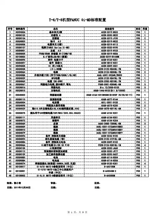
AOB416
- 格式:pdf
- 大小:299.95 KB
- 文档页数:5
Symbol
V
DSV
GSIDMIAREARTJ, TSTGSymbolTypMax8.1123340RθJL0.841.5Junction and Storage Temperature Range-55 to 175mJW50W°CRepetitive avalanche energy L=0.1mH C140Power Dissipation AAIDAvalanche Current C30A200Continuous Drain Current B,GMaximumUnitsParameterTC=25°C GTC=100°C B3011078TA=25°CPDSM3.1Power Dissipation BTC=25°CPD100TC=100°CTA=70°C2°C/WAbsolute Maximum Ratings TA=25°C unless otherwise notedVV±20Pulsed Drain Current Gate-Source VoltageDrain-Source Voltage
Maximum Junction-to-Ambient ASteady-StateMaximum Junction-to-Lead CSteady-State°C/WThermal CharacteristicsParameterUnitsMaximum Junction-to-Ambient At ≤ 10sRθJA°C/WAOB416N-Channel Enhancement Mode Field Effect TransistorFeaturesVDS (V) = 30VID = 110A (VGS = 10V)RDS(ON) < 4.5mΩ (VGS = 10V) @ 30ARDS(ON) < 6.5mΩ (VGS = 4.5V) @ 30AGeneral DescriptionThe AOB416 uses advanced trench technology to provide excellent RDS(ON), shoot-through immunity and body diode characteristics. This device is ideally suited for use as a low side switch in CPU core power conversion. Standard Product AOB416 is Pb-free (meets ROHS & Sony 259 specifications). AOB416L is a Green Product ordering option. AOB416 and AOB416L are electrically identical.G D S G D STO-263D2-PAKTop ViewDrain Connected to Tab
Alpha & Omega Semiconductor, Ltd.AOB416SymbolMinTypMaxUnitsBVDSS30V1TJ=55°C5IGSS100nAVGS(th)1.21.82.4VID(ON)110A3.54.5TJ=125°C5.36.55.156.5mΩgFS94SVSD0.641VIS110A
Ciss6060pFCoss638pFCrss355pFRg0.45ΩQg(10V)96.4nCQg(4.5V)46.4nCQgs13.6nCQgd16nCtD(on)15.5nstr28.2nstD(off)52.5nstf31nstrr31.2nsQrr19.3nCTHIS PRODUCT HAS BEEN DESIGNED AND QUALIFIED FOR THE CONSUMER MARKET. APPLICATIONS OR USES AS CRITICAL COMPONENTS IN LIFE SUPPORT DEVICES OR SYSTEMS ARE NOT AUTHORIZED. AOS DOES NOT ASSUME ANY LIABILITY ARISINGOUT OF SUCH APPLICATIONS OR USES OF ITS PRODUCTS. AOS RESERVES THE RIGHT TO IMPROVE PRODUCT DESIGN,FUNCTIONS AND RELIABILITY WITHOUT NOTICE.Gate Drain ChargeVGS=0V, VDS=15V, f=1MHzSWITCHING PARAMETERSTotal Gate ChargeGate Source ChargeGate resistanceVGS=0V, VDS=0V, f=1MHzTotal Gate ChargeVGS=4.5V, VDS=15V, ID=30ATurn-On Rise TimeTurn-Off DelayTimeVGS=10V, VDS=15V, RL=0.5Ω, RGEN=3ΩTurn-Off Fall TimeTurn-On DelayTimemΩVGS=4.5V, ID=30A IS=1A,VGS=0VVDS=5V, ID=30AMaximum Body-Diode Continuous CurrentInput CapacitanceOutput CapacitanceDYNAMIC PARAMETERSRDS(ON)Static Drain-Source On-ResistanceForward TransconductanceDiode Forward VoltageIDSSµAGate Threshold VoltageVDS=VGS ID=250µAVDS=24V, VGS=0V VDS=0V, VGS= ±20VZero Gate Voltage Drain CurrentGate-Body leakage currentElectrical Characteristics (TJ=25°C unless otherwise noted)STATIC PARAMETERSParameterConditions
Body Diode Reverse Recovery TimeBody Diode Reverse Recovery ChargeIF=30A, dI/dt=100A/µsDrain-Source Breakdown VoltageOn state drain currentID=250µA, VGS=0V VGS=4.5V, VDS=5VVGS=10V, ID=30A Reverse Transfer CapacitanceIF=30A, dI/dt=100A/µsA: The value of R θJA is measured with the device mounted on 1in 2 FR-4 board with 2oz. Copper, in a still air environment with T A =25°C. The Power dissipation PDSM is based on steady-state R θJA and the maximum allowed junction temperature of 150°C. The value in any given application depends on the user's specific board design, and the maximum temperature of 175°C may be used if the PCB or heatsink allows it.B. The power dissipation PD is based on TJ(MAX)=175°C, using junction-to-case thermal resistance, and is more useful in setting the upper dissipation limit for cases where additional heatsinking is used. It is used to determine the current rating, when this rating falls below the package limit.C: Repetitive rating, pulse width limited by junction temperature TJ(MAX)=175°C.D. The R θJA is the sum of the thermal impedence from junction to case R θJC and case to ambient.E. The static characteristics in Figures 1 to 6 are obtained using <300 µs pulses, duty cycle 0.5% max.F. These tests are performed with the device mounted on 1 in 2 FR-4 board with 2oz. Copper, in a still air environment with T A=25°C. The SOA curve provides a single pulse rating. G. The maximum current rating is limited by the package current capability. Rev 4 : June 2005Alpha & Omega Semiconductor, Ltd.AOB416TYPICAL ELECTRICAL AND THERMAL CHARACTERISTICS0102030405060012345VDS (Volts)Figure 1: On-Region CharacteristicsID(A)VGS=3V10V3.5V4.5V010203040506011.522.533.54VGS(Volts)Figure 2: Transfer CharacteristicsID(A)
3.03.54.04.55.05.56.0020406080100ID (A)Figure 3: On-Resistance vs. Drain Current and Gate VoltageRDS(ON) (mΩ)
1.0E-051.0E-041.0E-031.0E-021.0E-011.0E+001.0E+011.0E+020.00.20.40.60.81.01.2VSD (Volts)Figure 6: Body-Diode CharacteristicsIS (A)25°C125°C0.811.21.41.61.80255075100125150175Temperature (°C)Figure 4: On-Resistance vs. Junction TemperatureNormalized On-ResistanceVGS=10VVGS=4.5V