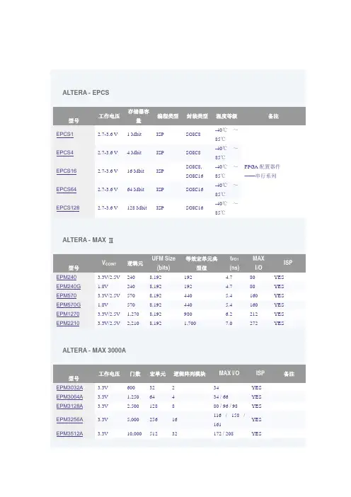
EPM2210
- 格式:pdf
- 大小:1.58 MB
- 文档页数:12
Dedicated Pin Information for the MAX IIEPM2210 / EPM2210G DevicesVersion 1.2Dedicated Pin 256-Pin FBGA 324-Pin FBGA IO/GCLK0H5J6IO/GCLK1J5K6IO/GCLK2J12K13IO/GCLK3H12J13IO/DEV_OE M8N9IO/DEV_CLRn M9N10TDI L6M7TMS N4P5TCK P3R4TDO M5N6GNDINT F7, G6, H7, H9, J8, J10, K11, L10G8, H7, J8, J10, K9, K11, L12, M11GNDIOA1, A16, B2, B15, G7, G8, G9, G10, K7, K8, K9, K10, R2, R15, T1, T16A1, A18, B2, B17, H8, H9, H10, H11, L8, L9, L10, L11, U2, U17, V1, V18VCCINT (1)F10, G11, H8, H10, J7, J9, K6, L7G11, H12, J9, J11, K8, K10, L7, M8VCCIO1 (2)C1, H6, J6, P1C1, J7, K7, T1VCCIO2 (2)A3, A14, F8, F9A3, A16, G9, G10 VCCIO3 (2) C16, H11, J11, P16C18, J12, K12, T18VCCIO4 (2)L8, L9, T3, T14M9, M10, V3, V16No Connect (N.C.)--Total User I/O Pins 204272Notes:1. For EPM2210 devices, all VCCINT pins must be connected to either 3.3V or2.5V (but not a combination of both). For EPM2210G devices, all VCCINT pins must be connected to 1.8V.2. Each set of VCCIO pins (VCCIO1, VCCIO2, etc.) can be connected to3.3V, 2.5V, 1.8V, or 1.5V.I/O Pin Information for the MAX IIEPM2210 / EPM2210G DevicesVersion 1.2Bank Number Pad Number Orientation Pin/Pad Function Optional Function(s)256-Pin FBGA 324-Pin FBGAB10VCCIO1B11GNDIO B12IO C2B13IO D3C3B14IOC2D25VCCINT B16IO D1B17IO D3B18IO C3E2B19IO E3D4B110IO D2E1B111IO E4E3B112IO D1F3B113IO E5E4B114IOE2F2B115VCCIO1B116GNDIO B117IO E5B118IO F1B119IO F4B120IO G3B121IO F5B122IO G2B123IO F3F6B124IO E1G1B125IO F4G4B126IO F2H3B127IO F5G5B128IO F1H2B129IO F6G6B130IO G2H1B131IO G3G7B132IOG1J3B133VCCIO1B134GNDIO B135IO G4H4B136IO H2J2B137IO G5H5B138IO H1J1B139IO H3H6B140IOJ1K141GNDINT B142IOGCLK0H5J643VCCINT B144IO GCLK1J5K6B145IOH4J4B146IO J2K2 B147IO J4J5 B148IO K1K3 B149IO K5 B150IO L1 B151VCCIO1B152GNDIOB153IO J3K4 B154IO K2L2 B155IO K5L6 B156IO L1L3 B157IO K4L5 B158IO M1 B159IO L4 B160IO L2M2 B161IO K3M6 B162IO M1M3 B163IO L5M5 B164IO M2N1 B165IO L4M4 B166IO N2 B167IO L3N5 B168IO N3 B169VCCIO1B170GNDIOB171IO N4 B172IO N1P1 B173IO M4P4 B174IO N2P2 B175IO M3P3 B176IO R1 77GNDINTB178IO N3R2 B179IO R3 B180TMS N4P5 B181TDI L6M7 B182TCK P3R4 B183TDO M5N6 B184IO P2T2 B185IO T3 B186VCCIO1B187GNDIOB188N.C. (1)B489VCCIO4B490GNDIOB491IO U1 92VCCINTB493IO R1V2 B494IO P4R5 B495IO T2U3 B496IO P5P6B497IO R3T4 B498IO N5R6 B499IO U4 B4100IO T6 B4101IO V4 B4102IO N7 B4103IO T5 B4104IO P7 B4105GNDIOB4106VCCIO4B4107IO R4U5 B4108IO P6R7 B4109IO T4V5 B4110IO N6T7 B4111IO R5U6 B4112IO M6N8 B4113IO T5V6 B4114IO P7P8 B4115IO R6U7 B4116IO N7R8 B4117IO T6V7 B4118IO M7T8 B4119IO R7U8 B4120VCCIO4B4121GNDIOB4122IO P8P9 B4123IO T7V8 B4124IO N8R9 B4125IO R8U9 B4126IO N9T9 B4127IO T8V9 128GNDINTB4129IO T9U10 130VCCINTB4131IO R9V10 B4132IO P9P10 B4133IO T10U11 B4134IO DEV_OE M8N9 B4135IO DEV_CLRn M9N10 B4136IO M10R10 B4137IO R10V11 B4138VCCIO4B4139GNDIOB4140IO N10T10 B4141IO T11U12 B4142IO P10N11 B4143IO R11V12 B4144IO M11P11 B4145IO T12U13 B4146IO N11R11 B4147IO R12V13B4148IO P11T11 B4149IO T13T14 B4150IO M12N12 B4151IO R13U14 B4152VCCIO4B4153GNDIOB4154IO N12P12 B4155IO R14V14 B4156IO P12R12 B4157IO T15T15 B4158IO T12 B4159IO U15 B4160IO P13 B4161IO V15 B4162IO R13 B4163IO U16 B4164IO T13 B4165IO V17 166GNDINTB4167IO R16U18 B4168IO P13R14 B4169VCCIO4B4170GNDIOB3171VCCIO3B3172GNDIOB3173IO T17 B3174IO R15 B3175IO P14T16 176VCCINTB3177IO R16 B3178IO P15 B3179IO P15R17 B3180IO N13P14 B3181IO R18 B3182IO N15 B3183IO P16 B3184IO N14 B3185IO N14P17 B3186IO M14N13 B3187IO N15P18 B3188IO M13M15 B3189IO N16N16 B3190VCCIO3B3191GNDIOB3192IO M14 B3193IO N17 B3194IO L14M13 B3195IO M15N18 B3196IO L13M12 B3197IO M16M16 B3198IO L12L16B3199IO L15M17 B3200IO L11L15 B3201IO L16M18 B3202IO K14L14 B3203IO K15L17 B3204IO K13L13 B3205IO K16L18 B3206VCCIO3B3207GNDIOB3208IO K12K16 B3209IO J15K17 B3210IO J14K15 B3211IO J16K18 B3212IO J13K14 B3213IO GCLK2J12K13 214VCCINTB3215IO GCLK3H12J13 216GNDINTB3217IO H16J18 B3218IO H13J14 B3219IO H15J17 B3220IO H14J15 B3221IO G16H18 B3222IO G12J16 B3223GNDIOB3224VCCIO3B3225IO G15H17 B3226IO G13H13 B3227IO F16G18 B3228IO G14H14 B3229IO F15G17 B3230IO F11H15 B3231IO E16G16 B3232IO F12H16 B3233IO E15F18 B3234IO F13G12 B3235IO D16F17 B3236IO F14G13 B3237GNDIOB3238VCCIO3B3239IO D15F16 B3240IO E12G14 B3241IO E18 B3242IO G15 B3243IO D14E17 B3244IO F13 B3245IO D18 B3246IO E13F14 B3247IO E16 B3248IO F15 B3249IO C15D17B3250IO E14 B3251IO D16 252GNDINTB3253IO C14C16 B3254IO E14E15 B3255IO C17 B3256IO D13D15 B3257N.C. (1)B3258VCCIO3B3259GNDIOB2260VCCIO2B2261GNDIO262VCCINTB2263IO B16B18 B2264IO C13D14 B2265IO A15A17 B2266IO C12E13 B2267IO B16 B2268IO D13 B2269IO C15 B2270IO F12 B2271IO B15 B2272IO E12 B2273IO A15 B2274IO D12 B2275GNDIOB2276VCCIO2B2277IO B14C14 B2278IO D12C12 B2279IO B13B14 B2280IO C11F11 B2281IO A13A14 B2282IO D11E11 B2283IO B12C13 B2284IO E11D11 B2285IO A12B13 B2286IO C10C11 B2287IO B11A13 B2288IO D10F10 B2289GNDIOB2290VCCIO2B2291IO A11B12 B2292IO E10E10 B2293IO B10A12 B2294IO C9D10 B2295IO A10B11 B2296IO D9C10 B2297IO B9A11 B2298IO E9C9 B2299IO A9B10 300VCCINTB2301IO A8A10 302GNDINTB2303IO B8A9 B2304IO E8D9 B2305IO A7B9 B2306IO D8E9 B2307IO B7A8 B2308IO C8F9 B2309GNDIOB2310VCCIO2B2311IO A6B8 B2312IO E7C8 B2313IO B6A7 B2314IO D7D8 B2315IO A5B7 B2316IO C7E8 B2317IO B5A6 B2318IO E6F8 B2319IO A4B6 B2320IO D6C7 B2321IO B4A5 B2322IO C6D7 B2323IO C4B5 B2324IO C5E7 B2325GNDIOB2326VCCIO2B2327IO B3C5 B2328IO D5F7 B2329IO A4 B2330IO C6 B2331IO B4 B2332IO D6 B2333IO C4 B2334IO E6 B2335IO A2B3 336GNDINTB2337IO B1A2 B2338IO D4D5 B2339IO B1 B2340VCCIO2B2341GNDIONotes: 1. No ConnectPin Description Information for the MAX® II and MAX® IIG DevicesVersion 1.2 Pin Name Pin Type Pin DescriptionSupply and Reference pinsVCCIO[1..4]Power I/O supply voltage pins for banks 1 through 4 respectively. EPM2210 and EPM1270 use VCCIO[1..4] while EPM240 and EPM570 use VCCIO[1..2]. Each VCCIO bank supports a different voltage level with the VCCIO pins providing power for the input and output buffers within that particular I/O bank. Each VCCIO bank can be powered with either 3.3 V, 2.5 V, 1.8 V or 1.5 V.GNDIO Ground Ground pins for all the I/O banks. VCCINT Power Voltage supply pins for the device. GNDINT Ground Ground pins for the internal supply.Programming and JTAG pinsDEV_CLRn I/O Dual-purpose pin that can override all clears on all device registers. All registers are cleared when the pin is driven low and all registers behave as defined in the design when this pin is driven high. If not used for its dual-purpose function this pin is a regular I/O.DEV_OE I/O Dual-purpose pin that can override all tri-states on the device. All output pins are tristated when the pin is driven low and all output pins behave as defined in the design when this pin is driven high. If not used for its dual-purpose function this pin is a regular I/O.TCK Input Dedicated JTAG input pin.TDI Input Dedicated JTAG input pin.TMS Input Dedicated JTAG input pin.TDO Output Dedicated JTAG output pin.Clock PinsGCLK [0..3]I/O Dual-purpose clock pins that connect to the global clock network. If not used forits dual-purpose function this pin is a regular I/O.Figure 1. MAX II EPM2210 / EPM2210G F256 Device Top View Package Diagram and Bank InformationPackage Diagram and Bank Information for the MAX ® IIEPM2210 / EPM2210G DevicesVersion 1.2Figure 2. MAX II EPM2210 / EPM2210G F324 Device Top View Package Diagram and Bank InformationPackage Diagram and Bank Information for the MAX ® IIEPM2210 / EPM2210G DevicesVersion 1.2The table below shows the revision historyDate/VersionChanges Made January 2005, v1.2Added MAX IIG Device Naming to Titles, Notes, and Figures July 2004, v1.1Added Package Diagram and Bank Information Figures for Each Package May 2004, v1.0Initial Release Pin Information for the MAX ® II EPM2210 and EPM2210G DevicesRevision HistoryVersion 1.2。