低成本的13.56MHz 1000W 300V RF功率放大器
- 格式:pdf
- 大小:74.10 KB
- 文档页数:10
产品描述T166是一个用于远程无钥匙进入系统(RKE)的高性能的OOK/ASK发射器。
该芯片包括了一个功率放大器,单稳态电路和一个由内部压控振荡器控制的锁相环电路。
单稳态电路用来控制锁相环和功率放大器,使其在操作时可以快速启动。
应用领域•无钥匙进入系统•远程控制系统•车库门开启器•报警系统•安防系统•无线传感器产品特点•高集成的OOK/ASK发射器•高输出功率,3V/+12dBm•自动待机功能,当DIN无信号输入超过50ms时,电路进入自动待机状态,消耗电流小于1uA•宽输入电压范围,2.0V to5.0V•需要少量的外部元件•基于PLL锁相环的发射器,频率范围为:200MHz到450MHz•片上单稳态电路•适用于OOK/ASK调制的60dB射频占空系数•封装:SOT23-6框图应用电路1材料清单器件值单位315MHz433.92MHzX19.84375M13.56M HzR11K OhmR2100K Ohm*R30OhmR40OhmC3,C7100n FC4220p FC58.2p 6.8p FC615p12p FL1180n HL239n22n H注释:1.R3可选0~100欧姆电阻来调节输出功率,R3选择0欧姆电阻使用时不要用导线或焊锡直接相连来代替。
2.L2/C5/C6的值受PCB布局的影响。
应用电路2材料清单器件值单位315MHz433.92MHzX19.84375M13.56M HzR11K OhmR2100K Ohm*R30OhmR40OhmC3,C7100n FC410p FC68.2p 6.8p FL1470n680n HL2150n82n H注释:1.R3可选0~100欧姆电阻来调节输出功率,R3选择0欧姆电阻使用时不要用导线或焊锡直接相连来代替。
2.L2/C4/C6的值受PCB布局的影响。
简化电路3材料清单器件值单位315MHz433.92MHzX19.84375M13.56M HzC1,C227p FC4220p FC615p12p FL1180n HL239n22n H备注:此外围为简化版低成本使用方案,极限测试或恶劣环境下使用不保证其性能参数和稳定性(如发射功率、二次谐波等),仅供参考。
用户手册RIGOL文件编号UGF01000-11102008年12月PA1000系列功率放大器© 2008 北京普源精电科技有限公司版权所有RIGOL 版权信息1.北京普源精电科技有限公司版权所有。
2.本公司产品受已获准及尚在审批的中华人民共和国专利的保护。
3.本手册提供的信息取代以往出版的所有资料。
4.本公司保留改变规格及价格的权利。
注:RIGOL是北京普源精电科技有限公司的注册商标。
PA1000系列功率放大器用户手册IRIGOLPA1000系列功率放大器用户手册II一般安全概要了解下列安全性预防措施,以避免受伤,并防止损坏本产品或与本产品连接的任何产品。
为避免可能的危险,请务必按照规定使用本产品。
只有授权人员才能执行维修程序。
避免起火和人身伤害。
使用正确的电源线。
只允许使用所在国家认可的本产品专用电源线。
将产品接地。
本产品通过电源的接地导线接地。
为避免电击,接地导体必须与地相连。
在连接本产品的输入或输出端之前,请务必将本产品正确接地。
查看所有终端额定值。
为避免起火和过大电流的冲击,请查看产品上所有的额定值和标记说明,请在连接产品前查阅产品手册以了解额定值的详细信息。
请勿开盖操作。
外盖或面板打开时,请勿运行本产品。
避免电路外露。
电源接通后,请勿接触外露的接头和元件。
怀疑产品出故障时,请勿进行操作。
如果您怀疑本产品已经出故障,可请RIGOL 授权的专业维修人员进行检查。
保持适当的通风。
请勿在潮湿环境下操作。
请勿在易燃易爆的环境下操作。
请保持产品表面的清洁和干燥。
RIGOLPA1000系列功率放大器用户手册III安全术语和符号本手册中的术语。
以下术语可能出现在本手册中:警告警告性声明指出可能会危害生命安全的条件和行为。
注意注意性声明指出可能导致本产品和其它财产损坏的条件和行为。
产品上的术语。
以下术语可能出现在产品上:危险表示您如果进行此操作可能会立即对您造成损害。
警告表示您如果进行此操作可能不会立即对您造成损害。
MRF 系列产品介绍(仅其中一部分)型号功能MRF581 5G 0.6WMRF181 800-1G 10WMRF182 1G 30WMRF281 800-2.6G 4WMRF282 2.6G 20WMRF284 800-2.6G 30W 带螺丝座MRF20060 1.7-2.6G 60WMRF9045 9G 45WMRF5003 520M 15WMRF5007 520M 15WMRF1517 520M 15WMRF1507 520M 15WMRF1511 175M 15WMRF1518 175M 15WMRF553 175M 1.5W33P50 520M 1W2SK2595 1G 10WMRF10005960-1215 MHz, 5.0 W, 28 V 微波功率晶体管MRF10031960-1215 MHz, 30 W (Peak), 36 V 微波功率晶体管MRF10120960-1215 MHz,W (Peak), 36 V 微波功率晶体管120MRF101501025-1150 MHz, 150 W (Peak), 50 V 微波功率晶体管MRF103501025-1150 MHz, 350 W (Peak), 50 V 微波功率晶体管MRF105021025-1150 MHz, 500 W (Peak), 50 V 微波功率晶体管MRF134达到400 MHz, 5.0 W, 28 V N 宽带射频功率MOSFETMRF136达到400 MHz, 15 W, 28 V N 宽带射频功率MOSFETMRF141175 MHz, 150 W, 28 V N 宽带射频功率 MOSFETMRF141GMRF148A30 W, 50 V N 宽带射频功率 MOSFETMRF150达到 150 MHz, 150 W, 50 V N 宽带射频功率 MOSFETMRF151175 MHz, 150 W, 50 V N 宽带射频功率 MOSFET MRF151G175 MHz, 300 W, 50 V N 宽带射频功率 MOSFET MRF15480 MHz, 600 W, 50 V N 宽带射频功率 MOSFETMRF157达到 80 MHz, 600 W, 50 V N 宽带射频功率 MOSFETMRF158达到 500 MHz, 2.0 W, 28 V TMOS N 宽带射频功率 FETMRF160500 MHz, 4.0 W, 28 V N 宽带射频功率 MOSFET MRF160061.6 GHz, 6.0 W, 28 V 射频功率晶体管 MRF160301.6 GHz, 30 W, 28 V RF 射频功率晶体管MRF166C500 MHz, 20 W, 28 V N 宽带射频功率 MOSFET MRF166W500 MHz, 40 W, 28 V TMOS N 宽带射频功率 FET MRF171A150 MHz, 45 W, 28 V N 宽带射频功率 MOSFET175 MHz, 300W, 28 V N 宽带射频功率 MOSFET达到 175 MHz,MRF173175 MHz, 80 W, 28 V N 宽带射频功率MOSFETMRF174200 MHz, 125 W, 28 V N 宽带射频功率MOSFETMRF177400 MHz, 100 W, 28 V N 宽带射频功率MOSFETMRF275G100 -500 MHz, 150 W, 28 V N 宽带射频功率MOSFETMRF275L500 MHz, 100 W, 28 V N 宽带射频功率MOSFETMRF42630 MHz, 25 W, 28 V 射频功率晶体管NPN SiMRF587500 MHz, 15 V, NF = 3.0 dB, 高频晶体管MRFIC1818 1.7-1.9G 2WMRF183 1G 45WMRF187 800-960MHz 85WMRF7042 900MHz 45WMRF175 400MHz 200WMRF581 5G 0.6W2SK2596 800-960MHz 1.5WBFG10 25G 0.6VBFG21 18G 4.5V 0.5A 0.6WBFG403 17G 4.5V 16MA 0.3WBFG410 22G 4.5V 12MA 135MWBFG425 25G 4.5V 30MA 135MWBFG450 45G 0.2WBFG540 45G 3V 30MA 35MWBFG541 9G 0.6WBLT81 800-960M 1.2WTP3022 800-960M 15WTDA1576 ICSRF7062 800-960M 150WMHL9236 800-960M 3WMHL7008 800-960M 3WMHL9128 800-960M 3WATF10136 4G 0.4WCMM2308 800-2.7G 1WCMM1330 1.7-1.9G 2WPF0030 860-915M 7W终端负载50 欧5W 3G,18G 驻波小于 1.06高频电阻50 欧100 欧30W 100W 3G型号技术指标数量单价(US$) 型号技术指标数量单价(US$)MRF281 800-2.6G 4W 4K 10 BFG10 25G 0.6W 10K 1MRF282 800-2.6G 10W 4K 15 BFG21 18G 4.5V 0.5A 0.6W 5K 1MRF284 800-2.6G 30W 带螺丝座4K 20 BFG403 17G 4.5V 16MA 0.3W 5K0.5MRF20060 1.7-2.6G 60W 6K 30 BFG410 22G 4.5V 12MA 135MW 5K 0.5MRF181 800-960M 10W 2K 10 BFG425 25G 4.5V 30MA 135MW 4K 0.5 MRF182 1G 30W 500PC 15 BFG450 45G 0.2W 1K 31.7-1.9G 2W 2K 10 BFG540 45G 3V 30MA 135MW 2K 3MRFIC1818MRF187 800-960M 85W 1K 30 BFG541 9G 0.6W 3K 0.5MRF7042 900M 45W 2K 15 BFG198 9G 1W 3K 0.5MRF9045 9G 45W 200PC 30 TP3022 800-960M 15W 4K 6MRF581 5G 0.6W 5K 0.5 TDA1576 IC 2K 2MRF5003 520M 15W 5K 3 SRF7062 800-960M 150W 2K 40MRF5007 520M 15W 5K 5 MHL9236 800-960M 3W 200PC 20MRF1517 520M 15W 2K 5 MHL7008 800-960M 3W 500PC 15MRF1507 520M 15W 2K 5 MHL9128 800-960M 3W 500PC 15MRF1511 175M 15W 2K 5 ATF10136 4G 0.4W 10K 1.5MRF1518 175M 15W 1K 5 CMM2308 800-2.7G 1W 10K 1.5MRF553 175M 1.5W 6K 0.5 CMM1330 1.7-1.9G 2W 5K 2MRF137 225MHz 30W 100PC 20 RF2125 1.5-2.2G 1W 1K 5MRF141 225MHZ 150W 100PC 40 PF0030 860-915M 7W 2K 2MRF151G 175MHz 300W 500PC 100 2SC1971 175MHz 7W 5KMRF154 150MHz 600W 500PC 200 2SC3356 6.5G 0.2W 5K 0.1MRF175G 500MHz 150W 500PC 100 2SC3357 6.5G 2W 5K 0.2MRF6404 1.8-2G 1K 10 2SC2407 500MHz 0.6W 10K 0.2BLT50 500M 1.2W 5K 0.6 2SC1906 1G 150MW 10K 0.05BLT81 400-960M 1.2W 3K 1 BLU98 5G 0.7W 5K 0.52SK2596 800-960M 1.5W 5K 0.5 33P55 800-960MHz 60W 5K 102SK2595 800-960M 10W 10K 3 E626 800-960Mhz 60W 5K 103SK228 1G 高放双栅管5K 0.15 终端负载50 欧5W 3G,18G 驻波小于 1.06 3K 10,100温补晶体12.8MHZ 贴片7x7M 5k 3 高频电阻50 欧100 欧30W 100W 3G 10kMRF9282 2A 7W 手持对讲机/ 长距离无绳电话/ 车载台/ 手机专用功率发射晶体管集成电路ICMC3361 10K 0.1 HT9200 5K 0.2MC33110 5K 0.2 HT9170 5K 0.2MC34119 5K 0.1 93C66 5K 0.1LM386 5K 0.1 24C08 5K 0.2M54958 5K 1.5 EM92547 5K 0.2M64082 5K 0.5 KA4588 5K 0.1TB31202 5K 0.4 KA567 5K 0.1手机功放及常用元件型号技术指标数量单价(US$) 型号技术指标数量单价(US$)MRFIC0913 800-1000MHZ 2W 现货面议AP109 900MHZ 2W 现货面议27E31 900MHZ 2W 现货面议AP119 1800MHZ 2W 现货面议08K38 900MHZ 2W 现货面议4370451 900MHZ 2W 现货面议08K40 900MHZ 2W 现货面议4370453 1800MHZ 2W 现货面议08K07 900MHZ 2W 现货面议TRF6053 900MHZ 2W 现货面议08K11 900MHZ 2W 现货面议TRF2253 频率合成IC 现货面议PF01420B 900MHZ 2W 现货面议13MHZ 温补晶体现货面议PF01412A 1800MHZ 2W 现货面议881-942 声表滤波器现货面议PF01411B 900MHZ 2W 现货面议PF014110B 1800MHZ 2W 现货面议常用元件MRF5711 8G 0.33W 现货面议BFQ67 8G 0.3W 现货面议MRF5811 5G 0.7W 现货面议BFG540 9G 0.4W 现货面议MMBR941 8G 0.25W 现货面议BFR182W 8G 0.3W 现货面议MMBR5031G 0.3W 现货面议BFR91 6G 0.3W 现货面议MMBR901 4G 0.3W 现货面议BU508 现货面议84UD22182EB-9C 现货面议Y759B 现货面议F741529AGHH 现货面议08122B 现货面议TWL3011GGM 现货面议089711747 现货面议LMST 现货面议LS28 现货面议。
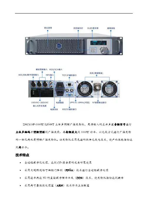
ZHC618F-1000W/LIGHT立体声调频广播发射机,是将输入的左右声道音频信号进行立体声编码并调频调制到广播波段、再射频放大到1000W功率、以无线方式进行广播发射的一体化高品质调频广播发射机。
该发射机采用先进的软件无线电技术,使产品性能指标达到高水平。
技术特点•全过程数字化处理,达到CD般音质的完美听觉效果•采用大规模现场可编程门阵列(FPGA)技术进行全过程数字处理•采用速率高达5G的直接数字频率合成(DDS)技术,使发射机指标达到巅峰•采用高可靠性微处理器(ARM)技术作为主控制器•支持多种音频信号源输入(发射机可按优先级自动选择):➢AES/EBU数字音频信号输入(最高优先级)➢模拟立体声模拟音频信号输入(第2优先级)➢MPX立体声复合信号输入(第3优先级)•支持RDS或SCA副载波输入•可升级为调频同步广播发射机•电控AGC控制输出功率零漂移•完善的过流、过压、过温、过功率、驻波比过大报警及保护功能•采用单键飞梭快速键盘输入•采用OLED实时显示工作参数•具备TCP/IP、RS232通信接口•19英寸标准机箱,高度2U工作原理框图主要技术参数电气指标1. 标称发射频率87MHz~108MHz(可定制其他频率),步进10kHz2. 载频允许偏差±200Hz3. 输出功率 0~1000W连续可调4. 输出功率允许偏差±1dB5. 输出阻抗 50Ω6. RF输出连接器L29/L27-50K(7/16”)或其他指定接头7. 残波辐射<-70dB8. 寄生调幅噪声<-50dB9. 导频频率偏差±0.1Hz10. S信号中38KHz残留分量<-50dB11. 100%调制频偏±75KHz(最大调制频偏112.5KHz)12. 音频预加重 0μs/25μs/ 50μs/75μs可选13. 信噪比≥92dB(1kHz,100%调制)14. 立体声分离度≥73dB (L→R,R→L)15. 失真度≤0.01%(30Hz~15000Hz,100%调制)16. 频率响应±0.01dB(不加重去重);±0.05dB(加去重)17. 左右声道电平差≤0.01dB(100%调制)18. 模拟音频输入-12dBm~+8dBm19. 模拟音频输入阻抗 600Ω平衡20. AES输入阻抗110Ω平衡21. AES输入电平0.2~10Vpp22. AES采样率30kHz~96kHz23. RDS输入阻抗10kΩ不平衡24. RDS输入电平0dBm25. MPX输入阻抗 10kΩ不平衡26. MPX输入电平 1.0Vpp27. 输入电平增益 -15dB~+15dB 步进0.1dB28. 散热方式强迫对流29. 电源电压100V AC~265V AC/ 47Hz~63Hz物理指标30. 机箱标准19英寸31. 机箱尺寸2U(宽445mm×高88mm×深500mm)32. 整机重量13.5Kg(含包装)33. 运行环境温度-10℃~+45℃34. 相对湿度<95%35. 海拔高度<4500m其他指标均满足GY/T 169—2001《米波调频广播发射机技术要求和测量方法》。
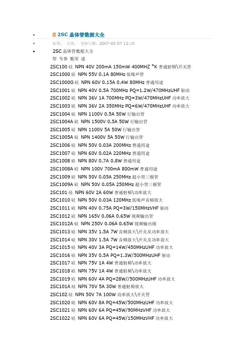
∙2SC晶体管数据大全∙标签:分类:更新日期:2007-02-07 12:10∙2SC晶体管数据大全型号参数用途2SC100硅NPN 40V 200mA 150mW 400MHZ *K普通射频\开关管 2SC1000硅NPN 55V 0.1A 80MHz低噪声管2SC1000G硅NPN 60V 0.15A 0.4W 80MHz普通用途2SC1001硅NPN 40V 0.5A 700MHz PQ=1.2W/470MHzUHF驱动 2SC1002硅NPN 36V 1A 700MHz PQ=3W/470MHzUHF功率放大 2SC1003硅NPN 36V 2A 350MHz PQ=6W/470MHzUHF功率放大 2SC1004硅NPN 1100V 0.5A 50W行输出管2SC1004A硅NPN 1500V 0.5A 50W行输出管2SC1005硅NPN 1100V 5A 50W行输出管2SC1005A硅NPN 1400V 5A 50W行输出管2SC1006硅NPN 50V 0.03A 200MHz普通用途2SC1007硅NPN 60V 0.02A 220MHz普通用途2SC1008硅NPN 80V 0.7A 0.8W普通用途2SC1008A硅NPN 100V 700mA 800mW普通用途2SC1009硅NPN 50V 0.05A 250MHz超小型三极管2SC1009A硅NPN 50V 0.05A 250MHz超小型三极管2SC101硅NPN 60V 2A 60W普通射频\功率放大2SC1010硅NPN 50V 0.03A 120MHz低噪声音频放大2SC1011硅NPN 40V 0.75A PQ=3W/150MHzVHF驱动2SC1012硅NPN 165V 0.06A 0.65W视频输出管2SC1012A硅NPN 250V 0.06A 0.65W视频输出级2SC1013硅NPN 35V 1.5A 7W音频放大\开关及功率放大2SC1014硅NPN 30V 1.5A 7W音频放大\开关及功率放大2SC1015硅NPN 40V 3A PQ=14W/450MHzUHF功率放大2SC1016硅NPN 35V 0.5A PQ=1.3W/500MHzUHF驱动2SC1017硅NPN 75V 1A 4W普通射频\功率放大2SC1018硅NPN 75V 1A 4W普通射频\功率放大2SC1019硅NPN 60V 4A PQ=28W//500MHzUHF功率放大2SC101A硅NPN 70V 5A 30W普通射频放大2SC102硅NPN 50V 7A 100W功率放大\开关管2SC1020硅NPN 60V 8A PQ=45W/500MHzUHF功率放大2SC1021硅NPN 60V 6A PQ=45W/90MHzVHF功率放大2SC1022硅NPN 60V 6A PQ=45W/150MHzVHF功率放大2SC1023硅NPN 25V 25mA 200MHz普通射频2SC1024硅NPN 50V 3A 25W音频放大\开关及功率放大2SC1025硅NPN 120V 3A 25W 铁壳音频放大\开关及功率放大2SC1026硅NPN 25V 0.025A 200MHz普通射频2SC1030A硅NPN 80V 6A 50W 10MHz普通射频放大2SC1030B硅NPN 80V 6A 50W 10MHz普通射频放大2SC1030C硅NPN 80V 6A 50W 10MHz普通射频放大2SC1030铁硅NPN 150V 6A 50W *K功率放大\开关管2SC1031硅NPN 300V 2A 30W功率放大\开关管2SC1032硅NPN 25V 0.025A 200MHz普通射频2SC1033硅NPN 200V 0.025A 0.3W视频输出管2SC1033A硅NPN 250V 25mA 300mW视频输出级2SC1034硅NPN 1100V 1A 25W功率放大\开关管2SC1035硅NPN 30V 0.02A 700MHz用于UHF频段及射频2SC1036硅NPN 30V 0.02A 700MHz用于UHF频段及射频2SC1037硅NPN 60V 4A PQ=33W/160MHzVHF功率放大2SC1038硅NPN 40V 150mA 3.75W PQ=0.8W/2.3GHzUHF驱动 2SC1039硅NPN 40V 250mA 7.5W PQ=1.4W/2.3GHzUHF驱动 2SC103A硅NPN 30V 80mA 250mW普通用途2SC104硅NPN 25V 50mA 250mW普通用途2SC1040硅NPN 45V 1.2A 15W PQ=8W/500MHzUHF功率放大2SC1041硅NPN 40V 150mA 3.75W PQ=0.9W/2GHzUHF驱动2SC1042硅NPN 40V 250mA 7.5W PQ=1.6/2GHzUHF驱动2SC1043硅NPN 45V 300mA 6W 2.2GHzUHF驱动2SC1044硅NPN 45V 30mA 250mW 1GHz用于UHF频段及射频 2SC1045硅NPN 1000V 1A 25W行输出管2SC1046硅NPN 1000V 3A 25W行输出管2SC1047硅NPN 30V 15mA 400mW 650MHz用于VHF频段及射频 2SC1048硅NPN 200V 0.05A 0.6W视频输出级2SC104A硅NPN 30V 80mA 250mW普通用途2SC105硅NPN 30V 80mA 250mW普通用途2SC1050硅NPN 300V 1A 40W功率放大\开关管2SC1051硅NPN 150V 7A 60W功率放大\开关管2SC1051H硅NPN 130V 7A 25W 8MHz高速管2SC1051L硅NPN 100V 7A 60W 8MHz高频放大2SC1052硅NPN 75V 1A 800mW <50/70ns开关管2SC1053硅NPN 75V 700mA 800mW >40/60ns开关管2SC1054硅NPN 35V 50mA 180mW 700MHzVHF低噪声放大2SC1055硅NPN 130V 7A 25W功率放大\开关管2SC1055H硅NPN 130V 7A 25W开关管2SC1056硅NPN 260V 100mA 750mW视频输出级2SC1057硅NPN 50V 1A 12W PQ=6.5W/700MHzUHF功率放大2SC1058硅NPN 50V 2A 20W PQ=11.5W/700MHzUHF功率放大2SC1059硅NPN 300V 150mA 8W功率放大\开关管2SC106硅NPN 60V 1.5A 15W音频放大\开关及功率放大2SC1060硅NPN 50V 3A 25W *K音频放大\开关及功率放大2SC1060A硅NPN 50V 3A 25W音频输出/放大管2SC1060B硅NPN 50V 3A 25W音频输出/放大管2SC1060C硅NPN 50V 3A 25W音频输出/放大管2SC1060D硅NPN 50V 3A 25W音频输出/放大管2SC1061硅NPN 50V 3A 25W *K音频放大\开关及功率放大2SC1061A硅NPN 50V 3A 25W音频输出/放大管2SC1061B硅NPN 50V 3A 25W音频输出/放大管2SC1061C硅NPN 50V 3A 25W音频输出/放大管2SC1061D硅NPN 50V 3A 25W音频输出/放大管2SC1062硅NPN 200V 100mA 700mW视频输出级2SC1063硅NPN 10V 1A 750mW普通用途2SC1064硅NPN 60V 1A 0.8W开关管2SC1065硅NPN 90V 1A 800mW开关管2SC1066硅NPN 20V 25mA 200mW 800MHz用于UHF频段及射频2SC1067硅NPN 35V 50mA 180mW 500MHz用于VHF频段及射频2SC1068硅NPN 25V 150mA 600mW 1.8GHzUHF驱动2SC1069硅NPN 00V 1A 800mW <60/120ns开关管2SC107硅NPN 60V 1A 15W音频放大\开关及功率放大2SC1070硅NPN 30V 20mA 150mW 900MHz用于UHF频段及射频2SC1070B硅NPN 30V 0.02A 900MHz用于UHF频段及射频2SC1071硅NPN 30V 200mA 300mW <45/42ns开关管2SC1072硅NPN 60V 700mA 800mW <40/60ns *K开关管2SC1072A硅NPN 66V 700mA 800mW <40/60ns开关管2SC1073硅NPN 36V 500mA 2W PQ=1.8W/500MHzUHF驱动2SC1074硅NPN 36V 1A 10W PQ=4W/500MHzUHF驱动2SC1075硅NPN 36V 2A PQ=15W/500MHzUHF功率放大2SC1076硅NPN 36V 3A 30WUHF功率放大2SC1077硅NPN 65V 5A 50W 150MHz PQ=42W/175MHzVHF功率放大2SC1077A硅NPN 65V 6A 60WVHF功率放大2SC1078硅NPN 700V 500mA 20W功率放大\开关管2SC1079硅NPN 150V 12A 100W音频放大\开关及功率放大2SC108硅NPN 90V 600mA 600mW普通射频\开关管2SC1080硅NPN 110V 12A 100W音频放大\开关及功率放大2SC1081硅NPN 40V 2.5A 30W PQ=14W/500MHzUHF功率放大 2SC1082硅NPN 50V 500mA 7W 1GHz PQ=3W/700MHzUHF驱动 2SC1083硅NPN 40V 500mA 3W 1.6GHzUHF驱动2SC1084硅NPN 35V 50mA 250mW 300MHz普通射频2SC1085硅NPN 30V 100mA 200mW 230MHz低噪声管2SC1086硅NPN 1000V 4A 125W行输出管2SC1087硅NPN 45V 3A 25W 1GHz普通射频\功率放大2SC1088硅NPN 300V 100mA 12.5W视频输出级2SC1089硅NPN 300V 0.1A 12.5W开关电源?2SC108A硅NPN 90V 0.8A 0.8W普通射频\开关管2SC109硅NPN 50V 600mA 600mW普通射频\开关管2SC1090硅NPN 20V 0.05A 3GHz用于UHF频段及射频2SC1092硅NPN 150V 0.7A 0.8W普通用途2SC1095硅NPN 30V 2A 10W功率放大用2SC1096硅NPN 40V 2A 10W *K音频放大\开关及功率放大2SC1097硅NPN 60V 1A 10W功率放大用2SC1098硅NPN 70V 1A 10W *K音频放大\开关及功率放大2SC1098A硅NPN 70V 3A 10W功率.开关电?2SC1099硅NPN 1200V 4.5A 50W行输出管2SC109A硅NPN 70V 800mA 600mW普通射频\开关管2SC11锗NPN 18V 24mA 0.055W开关管2SC110硅NPN 40V 200mA 750mW普通用途2SC1100硅NPN 1100V 4.5A 50W行输出管2SC1101硅NPN 1100V 1A 50W行输出管2SC1102硅NPN 300V 100mA 11W功率放大\开关管2SC1103硅NPN 250V 100mA 800mW视频输出级2SC1103A硅NPN 250V 100mA 800mW视频输出级2SC1104硅NPN 300V 1.5A 20W功率放大\开关管2SC1105硅NPN 300V 100mA 15W视频输出级2SC1106硅NPN 350V 3A 80W功率放大\开关管2SC1107硅NPN 80V 4A 25W音频放大\开关及功率放大2SC1108硅NPN 100V 4A 25W音频放大\开关及功率放大2SC1109硅NPN 80V 4A 25W音频放大\开关及功率放大2SC111硅NPN 50V 200mA 750mW普通用途2SC1110硅NPN 100V 4A 25W音频放大\开关及功率放大2SC1111硅NPN 140V 6A 50W音频放大\开关及功率放大2SC1112硅NPN 160V 6A 50W音频放大\开关及功率放大2SC1113硅NPN 120V 6A 40W音频放大\开关及功率放大2SC1114硅NPN 300V 4A 100W普通用途2SC1115硅NPN 140V 10A 100W *K功率放大\开关管2SC1116硅NPN 180V 10A 100W *K功率放大\开关管2SC1116A硅NPN 200V 10A 100W功率放大\开关管2SC1117硅NPN 20V 20mA 150mW 850MHz用于UHF频段及射频2SC1118硅NPN 45V 2A 27W PQ=14.5W/500MHzUHF功率放大2SC1119硅NPN 20V 30mA 250mW 4.5GHz用于UHF频段及射频2SC112硅NPN 40V 0.2A 0.75W普通用途2SC1120硅NPN 35V 1.5A 10W 700MHz PQ=4W/470MHzUHF功率放大 2SC1121硅NPN 35V 3A 20W 500MHz PQ=8.5W/470MHzUHF功率放大 2SC1122硅NPN 35V 4.5A 30W 400MHz PQ=14W/470MHzUHF功率放大 2SC1122A硅NPN 35V 4.5A 30W 400MHz PQ=14W/470MHzUHF功率放大 2SC1123硅NPN 35V 100mA 300mW 550MHz用于VHF频段及射频2SC1124硅NPN 140V 1A 7.9W音频放大\开关及功率放大2SC1126硅NPN 30V 50mA 250mW 550MHz用于VHF频段及射频2SC1127硅NPN 180V 100mA 7.9W视频输出级2SC1127-1硅NPN 180V 0.1A 0.95W普通用途2SC1127-2硅NPN 180V 0.1A 0.95W普通用途2SC1128硅NPN 35V 100mA 550W用于VHF频段及射频2SC1129硅NPN 35V 30mA 300mW 400MHz用于VHF频段及射频2SC113硅NPN 50V 0.2A 0.75W普通用途2SC1130硅NPN 800V 3.5A 80W功率放大\开关管2SC1131硅NPN 600V 3.5A 80W功率放大\开关管2SC1132硅NPN 1200V 2.5A 30W行输出管2SC1133硅NPN 1200V 5A 30W行输出管2SC1136硅NPN 200V 30A 200W功率放大\开关管2SC1138硅NPN 800V 30A 200W功率放大\开关管2SC1139硅NPN 600V 30A 200W开关管2SC113H硅NPN 50V 0.3A 0.75W 100MHz普通用途2SC114硅NPN 50V 200mA 750mW普通用途2SC1140硅NPN 800V 15A 150W开关管2SC1141硅NPN 600V 15A 150W开关管2SC1142硅NPN 800V 10A 125W开关管2SC1143硅NPN 600V 10A 125W开关管2SC1144硅NPN 400V 30A 200W功率放大\开关管2SC1145硅NPN 700V 20A 175W功率放大\开关管2SC115硅NPN 30V 50mA 750mW 200MHz普通用途2SC1150硅NPN 60V 1A <35/55ns开关管2SC1151硅NPN 900V 1A 50W行输出管2SC1151A硅NPN 1000V 1A 50W行输出管2SC1152硅NPN 300V 2.5A 50W功率放大\开关管2SC1153硅NPN 1200V 2.5A 50W行输出管2SC1153A硅NPN 1400V 2.5A 50W行输出管2SC1154硅NPN 1200V 3.5A 50W行输出管2SC1155硅NPN 70V 800mA 7W音频放大\开关及功率放大2SC1156硅NPN 90V 800mA 7W音频放大\开关及功率放大2SC1157硅NPN 110V 800mA 7W音频放大\开关及功率放大2SC1158硅NPN 35V 20mA 120mW 1.1GHz用于UHF频段及射频2SC1159硅NPN 35V 20mA 150mW 1.1GHz用于UHF频段及射频2SC116硅NPN 50V 200mA 750mW 120MHz普通用途2SC1160硅NPN 200V 1A 15W音频放大\开关及功率放大2SC1161硅NPN 200V 1A 15W音频放大\开关及功率放大2SC1162硅NPN 35V 2.5A 10W *K音频放大\开关及功率放大2SC1162拆硅NPN 35V 2.5A 10W2SC1163硅NPN 300V 100mA 20.8W视频输出\音频\功率放大2SC1164硅NPN 40V 300mA 600mW 1.4GHzUHF驱动2SC1165硅NPN 40V 500mA 700mW 600MHzUHF驱动2SC1166硅NPN 70V 200mA 600mW 120MHz *K普通用途2SC1167硅NPN 1200V 1.5A 50W行输出管2SC1168硅NPN 300V 150mA 12.5W2SC1169硅NPN 40V 1A 800mW 600MHz PQ>2.5W/175MHz普通射频或驱动2SC116H硅NPN 50V 0.2A 120MHz普通用途2SC116T硅NPN 75V 0.2A 0.75W 70MHz普通用途2SC117硅NPN 75V 600mA 13W功率放大\开关管2SC1170硅NPN 1200V 3.5A 50W行输出管2SC1170A硅NPN 1200V 3.5A 50W行输出管2SC1170B硅NPN 1500V 3.5A 50W行输出管2SC1171硅NPN 1100V 1A 50W行输出管2SC1172硅NPN 1500V 5A 50W行输出管2SC1172A硅NPN 1500V 7A 50W行输出管2SC1172B硅NPN 1500V 7A 50W行输出管2SC1173硅NPN 30V 3A 10W *K音频放大\开关及功率放大2SC1174硅NPN 1200V 3.5A 50W行输出管2SC1175硅NPN 50V 200mA 400mW 170MHz *K普通用途2SC1176硅NPN 40V 1A 15W PQ=7.5W/175MHzVHF功率放大2SC1177硅NPN 40V 2.5A 25W PQ=16W/175MHzVHF功率放大2SC1178硅NPN 40V 5A 35WVHF功率放大2SC1178A硅NPN 40V 5A 35W PQ=26W/175MHzVHF功率放大2SC117H硅NPN 75V 0.6A 13W开关管2SC117T硅NPN 75V 0.6A 2W 60MHz高频放大2SC118硅NPN 80V 600mA 13W功率放大\开关管2SC1180硅NPN 30V 20mA 150mW 800MHz用于UHF频段及射频2SC1181硅NPN 40V 50mA 300mW 400MHz普通射频\中频放大2SC1182硅NPN 25V 50mA 300mW 400MHz普通射频\中频放大2SC1184硅NPN 900V 1A 50W行输出管2SC1185硅NPN 300V 1.5A 50W功率放大\开关管2SC1187硅NPN 40V 30mA 250mW 600MHz射频\中频或自动增益控制2SC1188硅NPN 40V 30mA 250mW 850MHz普通射频\中频放大2SC1189硅NPN 50V 30mA 250mW 850MHz普通射频\中频放大2SC118H硅NPN 75V 0.6A 13W开关管2SC119硅NPN 75V 0.6A 13W功率放大\开关管2SC1190硅NPN 36V 2.5A 30W 600MHz PQ=16W/175MHzVHF功率放大 2SC1191硅NPN 36V 3.5A 45W PQ=27W/175MHzVHF功率放大2SC1192硅NPN 36V 5A 60W 350MHz PQ=37W/175MHzVHF功率放大2SC1193硅NPN 20V 30mA 200mW 4.5GHz用于UHF频段及射频2SC1195硅NPN 200V 2.5A 100W功率放大\开关管2SC1196硅NPN 60V 750mA 10W 800MHz PQ>3W/700MHzUHF功率放大 2SC1196A硅NPN 45V 1A 10W 1GHz PQ=5W/700MHzUHF功率放大2SC1197硅NPN 60V 2A 30W 700MHz PQ>9W/700MHzUHF功率放大2SC1197A硅NPN 45V 2A 20W 1GHz PQ=12W/700MHzUHF功率放大2SC1198硅NPN 45V 3.5A 30W 800MHz PQ=20W/700MHzUHF功率放大 2SC1199硅NPN 50V 300mA 600mW 1.4GHzUHF驱动2SC119H硅NPN 75V 0.6A 13W开关管2SC12锗NPN 60V 250mA 180mW低频开关管2SC120硅NPN 40V 25mA 250mW 200MHz普通用途2SC1200硅NPN 40V 180mA 2.5W 1.7GHzUHF驱动2SC1204硅NPN 30V 100mA 310mW 230MHz普通用途2SC1205硅NPN 30V 100mA 310mW 230MHz普通射频2SC1206硅NPN 45V 1.7A 25W PQ=10W/770MHzUHF功率放大 2SC1206A硅NPN 45V 1.7A PQ=10W/770MHzUHF功率放大2SC1206B硅NPN 45V 2A 25W PQ=12W/770MHzUHF功率放大 2SC1207硅NPN 45V 3A 30W PQ=16W/770MHzUHF功率放大 2SC1207A硅NPN 45V 3A PQ=16W/770MHzUHF功率放大2SC1207B硅NPN 45V 4A 50W PQ>19W/770MHzUHF功率放大 2SC1208硅NPN 36V 10A 60W PQ=37W/175MHzVHF功率放大 2SC1208A硅NPN 35V 10A 60W PQ>39W/175MHzVHF功率放大 2SC1209硅NPN 25V 700mA 500mW *K普通用途2SC121硅NPN 40V 25mA 250mW 130MHz普通用途2SC1210硅NPN 45V 500mA 500mW *K普通用途2SC1211硅NPN 65V 500mA 500mW *K普通用途2SC1212硅NPN 50V 1A 8W *K音频放大\开关及功率放大2SC1212A硅NPN 90V 1A 8W音频放大\开关及功率放大2SC1212AB硅NPN 80V 1A 8W 160MHz普通用途2SC1212AC硅NPN 80V 1A 8W 160MHz普通用途2SC1212B硅NPN 50V 1A 8W音频输出/放大管2SC1212C硅NPN 50V 1A 8W音频输出/放大管2SC1213硅NPN 35V 500mA 400mW *K普通用途2SC1213A硅NPN 50V 500mA 400mW *K普通用途2SC1213AB硅NPN 50V 0.5A 400mW普通用途2SC1213AC硅NPN 50V 0.5A 400mW普通用途2SC1213AD硅NPN 50V 0.5A 400mW普通用途2SC1213AKB硅NPN 50V 0.5A 400mW普通用途2SC1213AKC硅NPN 50V 0.5A 400mW普通用途2SC1213AKD硅NPN 50V 0.5A 400mW普通用途2SC1214硅NPN 50V 500mA 600mW普通用途2SC1214B硅NPN 50V 0.5A 0.6W普通用途2SC1214C硅NPN 50V 0.5A 0.6W普通用途2SC1214D硅NPN 50V 0.5A 0.6W普通用途2SC1215硅NPN 30V 0.2A 1.2GHz用于UHF频段及射频2SC1216硅NPN 40V 0.2A <20/40ns开关管2SC1217硅NPN 150V 300mA 750mW 250MHz *K开关管2SC1218硅NPN 80V 0.5A 370MHz普通射频\开关管2SC1219硅NPN 30V 0.5A 0.2W普通用途2SC122硅NPN 40V 25mA 250mW 160MHz普通用途2SC1220硅NPN 50V 0.5A 0.2W普通用途2SC1222硅NPN 60V 0.1A 100MHz *K低噪声管2SC1223硅NPN 30V 0.5A 1.3GHzUHF驱动2SC1224硅NPN 130V 0.8A 7W功率放大\开关管2SC1226硅NPN 40V 2A 10W *K音频放大\开关及功率放大2SC1226A硅NPN 50V 2A 10W *K音频放大\开关及功率放大2SC1227硅NPN 300V 10A 100W功率放大\开关管2SC1228硅NPN 500V 10A 100W功率放大\开关管2SC1229硅NPN 250V 10A 100W功率放大\开关管2SC123硅NPN 40V 25mA 250mW 180MHz普通用途2SC1230硅NPN 450V 10A 100W功率放大\开关管2SC1231硅NPN 20V 200mA 300mW 800MHz开关管2SC1232硅NPN 45V 1A 12W PQ=6W/700MHzUHF功率放大2SC1233硅NPN 45V 2A 20W PQ=11W/700MHzUHF功率放大2SC1235硅NPN 300V 100mA 6.5W视频输出级2SC1236硅NPN 20V 30mA 200mW 6.5GHz用于UHF频段及射频2SC1237硅NPN 85V 2A 10W 100MHz PQ=3.5W/27MHz普通射频\功率放大 2SC1238硅NPN 35V 150mA 5W 1.7GHUHF驱动2SC1239硅NPN 80V 4A 12.5W PQ=3.4W/27MHz普通射频或驱动2SC124硅NPN 40V 0.025A 200MHz普通用途2SC1240硅NPN 40V 50mA 350mW 600MHz普通射频2SC1241硅NPN 40V 1.5A 10W 400MHz PQ>6W/175MHzVHF功率放大2SC1241A硅NPN 35V 2A PQ=11W/175MHzVHF功率放大2SC1242硅NPN 40V 3A 20W 350MHz PQ=14W/175MHzVHF功率放大2SC1242A硅NPN 35V 4.5A 20W PQ=13W/175MHzVHF功率放大2SC1243硅NPN 25V 1.5A 7W *K音频放大\开关及功率放大2SC1244硅NPN 30V 50mA 200mW普通用途2SC1246硅NPN 30V 500mA 500mW普通用途2SC1247硅NPN 50V 500mA 500mW普通用途2SC1247A硅NPN 50V 500mA 500mW普通用途2SC1247AF硅NPN 50V 0.5A 500mW普通用途2SC1248硅NPN 20V 30mA 300mW 2.5GHz低噪声UHF放大2SC1249硅NPN 45V 0.3A 1.7GHzUHF驱动2SC125硅NPN 100V 50mA 750mW普通射频\开关管2SC1250硅NPN 45V 300mA 2.8W 1.9GHzUHF驱动2SC1251硅NPN 45V 300mA 7W 2.2GHzUHF驱动2SC1252硅NPN 45V 300mA 800mW 1.7GHzUHF驱动2SC1253硅NPN 45V 300mA 800mW 2GHzUHF驱动2SC1254硅NPN 45V 30mA 250mW 1GHz用于UHF频段及射频 2SC1255硅NPN 30V 100mA 3.5W >2.3GHUHF驱动2SC1256硅NPN 36V 800mA 5.5W PQ=3W/175MHzVHF驱动2SC1257硅NPN 36V 1.5A 14W PQ=8W/175MHzVHF功率放大 2SC1258硅NPN 36V 3A 28W PQ=14W/175MHzVHF功率放大2SC1259硅NPN 36V 3A 28W PQ=30W/175MHzVHF功率放大2SC126硅NPN 140V 50mA 750mW普通射频\开关管2SC1260硅NPN 45V 30mA 250mW 2GHz用于UHF频段及射频 2SC1261硅NPN 20V 20mA 300mW 2.5GHz用于UHF频段及射频 2SC1262硅NPN 45V 0.3A 1.7GHzUHF驱动2SC1263硅NPN 45V 0.3A 1.9GHzUHF驱动2SC1264硅NPN 30V 100mA 400mW 2GHz用于UHF频段及射频 2SC1265硅NPN 20V 50mA 300mW 3GHz对称孪生三极管2SC1266硅NPN 100V 1.5A 2W 150MHz开关管2SC1267硅NPN 45V 300mA 7W >1.8GHzUHF驱动2SC1268硅NPN 20V 50mA 250mW 6.5GHz用于UHF频段及射频 2SC1269硅NPN 20V 50mA 250mW 6.5GHz用于UHF频段及射频 2SC127硅NPN 20V 25mA 200mW 200MHz普通用途2SC1270硅NPN 20V 50mA 250mW 6.5GHz用于UHF频段及射频 2SC1271硅NPN 20V 30mA 200mW >6GHz用于UHF频段及射频 2SC1271A硅NPN 20V 30MA 250mW用于UHF频段及射频2SC1272硅NPN 20V 100mA 1W >3.3GHz用于UHF频段及射频 2SC1273硅NPN 20V 100mA 1W 1.5GHz用于UHF频段及射频2SC1274硅NPN 40V 300mA 300mW <80/86ns开关管2SC1275硅NPN 30V 50mA 250mW 2GHz用于UHF频段及射频 2SC1276硅NPN 40V 100mA 200mW <20/40ns开关管2SC1277硅NPN 60V 500mA 250mW普通用途2SC1278硅NPN 150V 50mA 250mW视频输出级2SC1278S硅NPN 150V 0.05A 0.25W视频输出管2SC1279硅NPN 180V 50mA 250mW视频输出级2SC1279S硅NPN 180V 0.05A 0.25W视频输出管2SC128锗NPN 30V 200mA 150mW开关管2SC1280硅NPN 15V 300mA 250mW β=20000达林顿管2SC1280A硅NPN 40V 300mA 250mW射频放大2SC1281硅NPN 20V 20mA 300mW 120MHz普通用途2SC1282硅NPN 70V 20mA 300mW普通用途2SC1283硅NPN 110V 20mA 300mW普通用途2SC1284硅NPN 30V 50mA 200mW 700MHz用于UHF频段及射频2SC1285硅NPN 40V 100mA 200mW 140MHz普通用途2SC1286硅NPN 25V 400MHz电视机中频放大2SC1288硅NPN 7V 60mA 200mW 4.5GHz高速开关管2SC129锗NPN 25V 200mA 150mW开关管2SC1290硅NPN 40V 200mA 740mW 1.5GHzUHF驱动2SC1292硅NPN 300V 2.5A 80W功率放大\开关管2SC1293硅NPN 25V 0.05A 400MHz普通射频2SC1295硅NPN 1000V 2A 40W行输出管2SC1296硅NPN 1300V 5A 50W行输出管2SC1297硅NPN 50V 3.5A 50W 190MHz PQ=26W/175MHzVHF功率放大 2SC1298硅NPN 50V 5A 80W 130MHz PQ=37W/175MHzVHF功率放大 2SC1299硅NPN 300V 30A 200W功率放大\开关管2SC13锗NPN 18V 0.04A 0.0 65W低频开关管2SC130硅NPN 60V 1A 20W射频\开关或功率放大2SC1300硅NPN 500V 30A 200W功率放大\开关管2SC1301硅NPN 250V 30A 200W功率放大\开关管2SC1302硅NPN 400V 30A 200W功率放大\开关管2SC1303硅NPN 40V 0.3A 200W 700MHzVHF驱动2SC1304硅NPN 300V 500mA 20W功率放大\开关管2SC1306硅NPN 65V 3A 12W 300MHz普通射频\功率放大2SC1307硅NPN 70V 8A 25W 150MHz普通射频\功率放大2SC1307-1硅NPN 70V 8A 150MHz普通射频放大2SC1308硅NPN 1500V 7A 50W行输出管2SC1309硅NPN 1200V 5A 80W行输出管2SC131硅NPN 40V 300mA 350MHz开关管2SC1310硅NPN 30V 0.1A 150MHz *K普通用途2SC1311硅NPN 30V 0.1A 150MHz普通用途2SC1312硅NPN 35V 0.1A 150MHz低噪声管2SC1313硅NPN 50V 0.1A 150MHz低噪声管2SC1314硅NPN 40V 5A 45W PQ=34W/175MHzVHF功率放大2SC1315硅NPN 35V 500mA 4W PQ=0.5W/150MHzVHF驱动2SC1316硅NPN 750V 1A 23W功率放大\开关管2SC1317硅NPN 30V 500mA 400mW *K普通用途2SC1317NC硅NPN 30V 0.5A 0.65W 200MHz高速管2SC1317拆硅NPN 30V 500mA 400mW *K普通用途2SC1318硅NPN 60V 0.5A 0.4W *K普通用途2SC1318A功率放大2SC1319硅NPN 40V 25mA 250mW 600MHz普通射频\中频放大 2SC132硅NPN 20V 300mA 350MHz开关管2SC1320硅NPN 50V 30mA 250mW 850MHz普通射频\中频放大 2SC1321硅NPN 30V 10mA 100mW 1GHz超小型的UHF管2SC132102硅NPN 30V 0.01A 0.1W 900MHz用于UHF频段及射频 2SC132103硅NPN 30V 0.01A 0.1W 900MHz用于UHF频段及射频 2SC132104硅NPN 30V 0.01A 0.1W 900MHz用于UHF频段及射频 2SC132105硅NPN 30V 0.01A 0.1W 900MHz用于UHF频段及射频 2SC1322硅NPN 250V 15A 100W功率放大\开关管2SC1323硅NPN 30V 500mA 5W 1.3GHzUHF驱动2SC1324硅NPN 35V 150mA 800mW 1.7GH行输出管2SC1325硅NPN 1500V 6A 8W行输出管2SC1325A硅NPN 1500V 6A 8W开关电路2SC1326硅NPN 30V 400mA 5W 700MHzVHF驱动2SC1327硅NPN 35V 50mA 400mW 250MHz *K普通用途2SC1328硅NPN 55V 50mA 400mW 250MHz *K普通用途2SC1329硅NPN 50V 8A 60W PQ=32W/70MHz普通射频\功率放大 2SC133硅NPN 20V 300mA 350MHz开关管2SC1330硅NPN 50V 100mA 400mW普通用途2SC1331硅NPN 20V 20mA 150mW 750MHz用于UHF频段及射频 2SC1333硅NPN 45V 1A 10W 1.2GHzUHF驱动2SC1334硅NPN 45V 1A 11.6W >1GHzUHF驱动2SC1335硅NPN 30V 100mA 200mW 230MHz低噪声管2SC1336硅NPN 20V 0.025A 4.5MHz用于UHF频段及射频2SC1337硅NPN 35V 2A 20W PQ=8.5W/485MHzUHF功率放大2SC1338硅NPN 35V 3A 30W PQ=16W/485MHzUHF功率放大2SC1339硅NPN 35V 5A 40W PQ=28W/485MHzUHF功率放大2SC134硅NPN 40V 300mA 350MHz开关管2SC1340硅NPN 35V 1A 5W 1GHzUHF驱动2SC1342硅NPN 30V 30mA 100mW 250MHz普通射频2SC1342A硅NPN 30V 0.03A 0.1W 320MHz高频管2SC1342B硅NPN 30V 0.03A 0.1W 320MHz高频管2SC1342C硅NPN 30V 0.03A 0.1W 320MHz高频管2SC1343硅NPN 150V 10A 100W *K音频放大\开关及功率放大 2SC1343H硅NPN 130V 10A 100W 15MHz高速管2SC1344硅NPN 30V 100mA 200mW 230MHz低噪声管2SC1344D硅NPN 30V 0.1A 230MHz普通用途2SC1344E硅NPN 30V 0.1A 230MHz普通用途2SC1344F硅NPN 30V 0.1A 230MHz普通用途2SC1345硅NPN 55V 100mA 200mW 230MHz低噪声管2SC1345D硅NPN 55V 0.1A 230MHz普通用途2SC1345E硅NPN 55V 0.1A 230MHz普通用途2SC1345F硅NPN 55V 0.1A 230MHz普通用途2SC1345KD硅NPN 55V 0.1A 230MHz普通用途2SC1345KE硅NPN 55V 0.1A 230MHz普通用途2SC1345KF硅NPN 55V 0.1A 230MHz普通用途2SC1346硅NPN 30V 0.5A 0.6W *K普通用途2SC1347硅NPN 60V 0.5A 0.6W *K普通用途2SC1348硅NPN 1000V 4A 125W行输出管2SC1348-1硅NPN 1000V 4A 125W用于电视机2SC1348-2硅NPN 1100V 4A 125W 5MHz用于电视机2SC1348-3硅NPN 1200V 4A 125W 5MHz用于电视机2SC1349硅NPN 20V 0.2A高速开关管2SC135硅NPN 20V 0.3A 350MHz开关管2SC1350硅NPN 25V 0.3A开关管2SC1351硅NPN 80V 1A 0.8W开关管2SC1352硅NPN 25V 0.8A 0.8W开关管2SC1353硅NPN 90V 0.7A 0.65W开关管2SC1354硅NPN 55V 5A PQ=37W/175MHzVHF功率放大2SC1355硅NPN 40V 0.7A 1.8GHz PQ=2W/700MHzUHF驱动 2SC1356硅NPN 40V 1A 1.8GHz PQ=6W/700MHzUHF功率放大 2SC1358硅NPN 1400V 4.5A 50W行输出管2SC1358A硅NPN 1400V 5.5A 50W行输出管2SC1359硅NPN 30V 0.03A 300MHz *K普通用途2SC136硅NPN 80V 300mA 350MHz开关管2SC1360硅NPN 50V 0.05A 500MHz普通射频\中频放大2SC1361硅NPN 25V 0.2A 140MHz普通用途2SC1362硅NPN 50V 0.2A 140MHz普通用途2SC1363硅NPN 25V 0.2A 140MHz普通用途2SC1364硅NPN 50V 0.2A 140MHZ普通用途2SC1365硅NPN 45V 0.3A 1.7GHZUHF驱动2SC1366硅NPN 45V 0.3A 2GHzUHF驱动2SC1367硅NPN 1000V 1A 50W行输出管2SC1367A硅NPN 1000V 1A 50W行输出管2SC1368硅NPN 25V 1.5A 8W *K音频放大\开关及功率放大2SC1369硅NPN 25V 30mA 250mW音频放大\普通射频2SC137硅NPN 25V 300mA 350MHz开关管2SC1372硅NPN 30V 0.2A 250MHz普通用途2SC1373硅NPN 25V 0.1A <100/325ns普通用途2SC1374硅NPN 25V 0.1A <14/32ns开关管2SC1374H硅NPN 25V 0.1A 0.3W 600MHz开关管2SC1375硅NPN 25V 0.1A <45/60ns开关管2SC1375H硅NPN 25V 0.1A 0.3W开关管2SC1376硅NPN 40V 0.15A <25/60ns开关管2SC1376H硅NPN 40V 0.5A 0.3W 500MHz开关管2SC1377硅NPN 90V 6A 100MHz PQ=8W/27MHz普通射频\功率放大 2SC1378硅NPN 40V 4A 150MHz PQ=25W/175MHzVHF功率放大 2SC1379硅NPN 40V 7A 150MHz PQ=40W/175MHzVHF功率放大 2SC138硅NPN 60V 500mA 800mW 400MHzVHF驱动2SC1380硅NPN 55V 0.1A 80MHz普通用途2SC1380A硅NPN 55V 100mA 200mW 80MHz普通用途2SC1381硅NPN 100V 1A 0.8W音频放大\开关及功率放大2SC1382硅NPN 80V 1A 0.8W *K音频放大\开关及功率放大2SC1383硅NPN 30V 1A 0.75W *K普通用途2SC1383 拆普通用途2SC1383NC硅NPN 30V 1A 1W 200MHz普通用途2SC1384硅NPN 60V 1A 0.75W *K普通用途2SC1384NC硅NPN 60V 1A 0.75W普通用途2SC1385硅NPN 60V 0.5A <40/60ns开关管2SC1385H硅NPN 60V 0.5A <40/60ns开关管2SC1386硅NPN 70V 0.7A <35/55ns开关管2SC1386H硅NPN 70V 1A 0.8W高频放大2SC1387硅NPN 25V 0.15A 1.6GHzUHF驱动2SC1388硅NPN 80V 1A 0.8W开关管2SC138A硅NPN 60V 500mA 800mW 400MHzVHF驱动2SC139硅NPN 60V 500mA 800mW 400MHzVHF驱动2SC1391硅NPN 300V 100mA 6.5W视频输出级2SC1393硅NPN 30V 20mA 250mW 700MHz普通射频\中频放大2SC1394硅NPN 30V 0.02A 700MHz普通射频\中频放大2SC1395硅NPN 30V 0.02A 1.1GHz用于UHF频段及射频2SC1396硅NPN 30V 0.02A 1.1GHz用于UHF频段及射频2SC1398硅NPN 70V 2A 15W *K音频放大\开关及功率放大2SC1398A硅NPN 70V 2A 15W射频.功率放?2SC1399硅NPN 100V 0.05A 100MHz普通用途2SC14锗NPN 18V 40mA 65mW低频开关管2SC140硅NPN 60V 1A 1.7W 150MHz普通用途2SC1400硅NPN 85V 0.05A 100MHz普通用途2SC1401硅NPN 400V 30A 200W功率放大\开关管2SC1402硅NPN 140V 8A 70W *K音频放大\开关及功率放大2SC1403硅NPN 160V 8A 70W *K音频放大\开关及功率放大2SC1403A硅NPN 180V 8A 70W音频放大\开关及功率放大2SC1404硅NPN 36V 3.5A 1GHz PQ=18W/470MHz *KUHF功率放大 2SC1405硅NPN 36V 0.75A PQ=3.52/175MHz *KVHF驱动2SC1406硅NPN 30V 1A 1W *K普通用途2SC1407硅NPN 60V 1A 1W *K普通用途2SC1409硅NPN 200V 2A 12.5W *K音频放大\开关及功率放大2SC1409A硅NPN 200V 2A 12.5W音频放大\开关及功率放大2SC141硅NPN 20V 200mA 360MW 450MHz普通射频\开关管2SC1410硅NPN 200V 2A 12.5W *K音频放大\开关及功率放大2SC1410A硅NPN 200V 2A 12.5W音频放大\开关及功率放大2SC1411硅NPN 6V 0.05A *K斩波器2SC1412硅NPN 45V 0.15A 1.5GHz *KUHF驱动2SC1413硅NPN 1200V 5A 50W *K行输出管2SC1413A硅NPN 1500V 5A 50W行输出管2SC1413A 拆?,硅NPN 1500V 5A 50W2SC1413AH硅NPN 1500V 5A 50W行输出管2SC1414硅NPN 40V 2A 1.5GHz PQ=10W/700MHzUHF功率放大2SC1415硅NPN 40V 3A 1.2GHz PQ=16W/700MHz *KUHF功率放大 2SC1416硅NPN 55V 0.05A 100MHz低噪声管2SC1416A硅NPN 55V 50mA 200mW 100MHz低噪声管2SC1417硅NPN 20V 0.03A 300MHZ普通射频2SC1418硅NPN 50V 2A 20W *K音频放大\开关及功率放大2SC1419硅NPN 50V 2A 20W *K音频放大\开关及功率放大2SC1420硅NPN 15V 0.07A 6GHz *K用于UHF频段及射频2SC1421硅NPN 15V 0.03A 5.5GHz *K用于UHF频段及射频 2SC1422硅NPN 15V 0.04A 5.5GHz *K用于UHF频段及射频 2SC1423硅NPN 15V 0.03A 7GHz *K用于UHF频段及射频2SC1424硅NPN 30V 0.05A 2GHz *K用于UHF频段及射频2SC1425硅NPN 45V 1A >1GHzUHF驱动2SC1426硅NPN 35V 0.2A 2.5GHzUHF驱动2SC1427硅NPN 30V 0.01A 1GHz超小型的UHF管2SC1428硅NPN 50V 0.05A 250MHz普通超小型管2SC1429硅NPN 12V 2A 0.95W低频开关管2SC1429-1硅NPN 16V 2A 0.95W 80MHz普通用途2SC1429-2硅NPN 16V 2A 0.95W 80MHz普通用途2SC1430硅NPN 110V 1.5A 0.5W低频开关管2SC1431硅NPN 110V 2A 23W音频放大\开关及功率放大2SC1431-1硅NPN 110V 2A 23W音频输出/放大管2SC1431-2硅NPN 140V 2A 23W 80MHz高速管2SC1432硅NPN 30V 0.3A β=40000达林顿管2SC1433硅NPN 600V 5A 50W功率放大\开关管2SC1434硅NPN 600V 15A 150W功率放大\开关管2SC1435硅NPN 600V 40A 300W功率放大\开关管2SC1436硅NPN 230V 15A 100W功率放大\开关管2SC1437硅NPN 230V 50A 200W *K功率放大\开关管2SC1438硅NPN 150V 0.05A 0.5W视频输出管2SC1439硅NPN 150V 0.05A 0.5W视频输出管2SC144硅NPN 50V 200mA 360mW 450MHz普通射频\开关管 2SC1440硅NPN 150V 15A 100W功率放大\开关管2SC1441硅NPN 200V 15A 100W功率放大\开关管2SC1442硅NPN 150V 50A 200W功率放大\开关管2SC1443硅NPN 200V 50A 200W功率放大\开关管2SC1444硅NPN 80V 6A 40W音频放大\开关及功率放大2SC1445硅NPN 100V 6A 40W音频放大\开关及功率放大2SC1446硅NPN 300V 0.1A 10W视频输出级2SC1447硅NPN 300V 0.15A 20W视频输出管2SC1448硅NPN 150V 1.5A 25W音频放大\开关及功率放大2SC1448A硅NPN 150V 1.5A 25W音频放大\开关及功率放大 2SC1449硅NPN 40V 2A 5W音频放大\开关及功率放大2SC145硅NPN 30V 200mA 360mW 500MHz普通射频\开关管2SC1450硅NPN 150V 0.4A 20W *K功率放大\开关管2SC1451硅NPN 150V 50mA 700mW视频输出级2SC1452硅NPN 150V 50mA 700mW视频输出级2SC1453硅NPN 55V 0.1A 150MHz普通用途2SC1454硅NPN 300V 4A 50W功率放大\开关管2SC1456硅NPN 300V 200mA 15W视频输出级2SC1457硅NPN 35V 150mA 800mW 2.7GHzUHF驱动2SC1458硅NPN 20V 50mA 300mW 3GHz *K用于UHF频段及射频2SC1459硅NPN 15V 70mA 300mW 5GHz *K用于UHF频段及射频2SC146硅NPN 50V 200mA 360mW 500MHz普通射频\开关管2SC1460硅NPN 15V 30mA 250mW 4.5GHz *K用于UHF频段及射频2SC1461硅NPN 15V 40mA 250mW 4.5GHz *K用于UHF频段及射频2SC1462硅NPN 15V 30mA 250mW 6.5GHz *K用于UHF频段及射频2SC1463硅NPN 450V 4A 75W *KVHF驱动2SC1464硅NPN 50V 500mA 4W 1.3GHz PQ=1.2W/175MHz *KVHF驱动 2SC1465硅NPN 50V 500mA 7W 1.6GHz PQ=1.8W/700MHz *KUHF驱动 2SC1466硅NPN 450V 3A 30W *K功率放大\开关管2SC1467硅NPN 500V 3A 30W *K功率放大\开关管2SC1468硅NPN 450V 10A 100W功率放大\开关管2SC1469硅NPN 500V 10A 100W功率放大\开关管2SC1469A硅NPN 500V 10A 100W功率放大\开关管2SC146A硅NPN 60V 200mA 175mW 500MHz普通射频\开关管2SC147硅NPN 30V 1A 750mW 120MHz普通用途2SC1470硅NPN 450V 30A 200W功率放大\开关管2SC1470LN硅NPN 40V 0.15A 0.30W放大管2SC1470S硅NPN 40V 0.15A 0.30W放大管2SC1470SLN硅NPN 40V 0.15A 0.30W放大管2SC1471硅NPN 500V 30A 200W功率放大\开关管2SC1471A硅NPN 500V 30A 200W功率放大\开关管2SC1472硅NPN 40V 300mA 500mW β=10000达林顿管2SC1472KA硅NPN 30V 0.3A 0.5W 50MHz普通用途2SC1472KB硅NPN 30V 0.3A 0.5W 50MHz普通用途2SC1473硅NPN 250V 0.07A 0.6W *K2SC1473A硅NPN 300V 70mA 750mW音频放大2SC1473NC硅NPN 250V 0.07A 0.75W 50MHz2SC1474硅NPN 16V 2A 750W *K普通用途2SC1474-3硅NPN 20V 2A 0.75W 80MHz普通用途2SC1474-4硅NPN 20V 2A 0.75W 80MHz普通用途2SC1475硅NPN 100V 1A 750mW *K普通用途2SC1476硅NPN 38V 5A 40W PQ=28W/470MHz *KUHF功率放大2SC1477硅NPN 230V 9A 80W *K功率放大\开关管2SC1478硅NPN 35V 50mA 150MHz *K普通用途2SC1478A硅NPN 55V 150mA 175mW 150MHz普通用途2SC1479硅NPN 36V 500mA 3W 1GHz PQ=1.2W/175MHz *KVHF驱动2SC147A硅NPN 30V 1A 0.75W 100MHz普通用途2SC147B硅NPN 60V 1A 0.75W 100MHz普通用途2SC1480硅NPN 36V 500mA 7W 1.2GHz PQ=2.4W/470MHz *KUHF驱动 2SC1481硅NPN 36V 1A 12W 1GHz PQ=5W/470MHz *KUHF功率放大2SC1482硅NPN 36V 2A 20W 800MHz PQ=8.5W/470MHz *KUHF功率放大 2SC1483硅NPN 20V 40mA 300mW 3GHz低噪声UHF放大2SC1485硅NPN 250V 125mA 350mW视频输出级2SC1486硅NPN 36V 400mA 5W PQ=2W/470MHzUHF驱动2SC1487硅NPN 36V 800mA 15W PQ=4W/470MHzUHF功率放大2SC1488硅NPN 36V 2A 37.5W PQ=10W/470MHz *KUHF功率放大2SC1489硅NPN 36V 6A 60W PQ=25W/470MHz *KUHF功率放大2SC149硅NPN 120V 300mA 800mW视频输出\开关管2SC1490硅NPN 36V 1A 12W PQ=4W/175MHz *KVHF驱动2SC1491硅NPN 36V 2.5A PQ=15W/175MHz *KVHF功率放大2SC1492硅NPN 36V 4A 65W PQ=25W/175MHz *KVHF功率放大2SC1493硅NPN 36V 4A 65W PQ=30W/175MHz *KVHF功率放大2SC1494硅NPN 36V 6A PQ=40W/175MHz *KVHF功率放大2SC1495硅NPN 36V 0.4A PQ=0.5W/470MHzUHF驱动2SC1496A硅NPN 35V 1.5A 1.2W功率放大2SC1498硅NPN 36V 2.5AUHF功率放大2SC1499硅NPN 36V 6AUHF功率放大2SC15硅NPN 30V 50mA 750mW普通用途2SC150硅NPN 20V 100mA 750mW 80MHz普通用途2SC15-0硅NPN 30V 0.05A 0.75W普通用途2SC1500硅NPN 36V 8A 115WUHF功率放大2SC1501硅NPN 300V 100mA 10W视频输出级2SC1503硅NPN 50V 3A 30W PQ=13W/260MHz *KVHF功率放大2SC1504硅NPN 400V 2A 40W功率放大\开关管2SC1505硅NPN 300V 200mA 15W视频输出级2SC1506硅NPN 300V 200mA 15W视频输出级2SC1507硅NPN 300V 0.2A 15W *K开关管2SC1507拆硅NPN 300V 0.2A 15W开关管2SC1509硅NPN 80V 500mA 1W *K普通用途2SC1509NC硅NPN 80V 0.5A 0.75W普通用途2SC150H硅NPN 20V 0.1A 0.75W 60MHz低频放大2SC150T硅NPN 50V 0.1A 0.75W 150MHz低频放大2SC151硅NPN 40V 100mA 750mW 100MHz普通用途2SC15-1硅NPN 60V 0.05A 0.75W普通用途2SC1510硅NPN 47V 1A 10W PQ=4.5W/770MHz *KUHF功率放大 2SC1511硅NPN 50V 3A 50W PQ=25W/275MHz *KVHF功率放大 2SC1512硅NPN 50V 5A 65.2W PQ=37W/275MHzVHF功率放大 2SC1513硅NPN 40V 300mA 800mW 1.8GHzUHF驱动2SC1514硅NPN 300V 0.1A 1.25W视频输出级2SC1515硅NPN 200V 50mA 200mW *K视频输出级2SC1515K硅NPN 200V 0.05A 0.2W视频输出管2SC1516硅NPN 35V 1.5A 10W *K低频开关管2SC1516K硅NPN 35V 1.5A 1.2W 110MHz普通用途2SC1516KB硅NPN 35V 1.5A 10W 110MHz高频放大2SC1516KC硅NPN 35V 1.5A 10W 110MHz高频放大2SC1517硅NPN 50V 1A 10W低频开关管2SC1517A硅NPN 80V 1A 10W低频开关管2SC1517AK硅NPN 80V 1A 1.2W 11MHz普通用途2SC1517AKB硅NPN 80V 1A 10W 150MHz高速管2SC1517AKC硅NPN 80V 1A 10W 150MHz高速管2SC1518硅NPN 25V 1A 750mW *K普通用途2SC1519硅NPN 250V 200mA 10W *K视频输出级2SC151H硅NPN 40V 0.1A 0.75W 100MHz普通用途2SC151HA硅NPN 40V 0.1A 0.75W 100MHz普通用途2SC151HB硅NPN 40V 0.1A 0.75W 100MHz普通用途2SC151HC硅NPN 40V 0.1A 0.75W 100MHz普通用途2SC152硅NPN 60V 100mA 750mW 120MHz普通用途2SC15-2硅NPN 90(120)V 0.05A 0.75W普通用途2SC1520硅NPN 250V 200mA 10W *K视频输出级2SC1521硅NPN 250V 200mA 10W *K视频输出级2SC1522硅NPN 250V 200mA 10W *K视频输出级2SC1523硅NPN 40V 300mA 3.5W 2GHz *KVHF驱动2SC1524硅NPN 50V 1A 12W 800MHz PQ=8W/700MHz *KUHF功率放大 2SC1525硅NPN 50V 2A 800MHz PQ=13W/700MHz *KUHF功率放大2SC1526硅NPN 50V 3A 25W 1GHz PQ=22W/700MHz *KUHF功率放大 2SC1528硅NPN 40V 2.5A 25W PQ=16W/175MHz *KVHF功率放大2SC1529硅NPN 30V 20mA 120mW *K用于UHF频段及射频2SC152H硅NPN 60V 0.1A 0.75W 120MHz普通用途2SC152HA硅NPN 60V 0.1A 0.75W 120MHz普通用途2SC152HB硅NPN 60V 0.1A 0.75W 120MHz普通用途2SC152HC硅NPN 60V 0.1A 0.75W 120MHz普通用途2SC153硅NPN 120V 100mA 750mW 140MHz普通用途2SC15-3硅NPN 90(120)V 0.05A 0.75W普通用途2SC1530硅NPN 50V 350mA 5W PQ=1.5W/1GHz用于UHF频段及射频2SC1532硅NPN 300V 30A 200mW *K功率放大\开关管2SC1533硅NPN 45V 1A 12W 1.8GHz PQ=2.2W/700MHz *KUHF驱动2SC1534硅NPN 45V 1A 12W 1.6GHz PQ=7W/700MHz *KUHF驱动2SC1535硅NPN 45V 2A 25W 1.2GHz PQ=12W/700MHz *KUHF功率放大 2SC1536硅NPN 45V 4A 40W 800MHz PQ=24W/700MHz *KUHF功率放大 2SC1537硅NPN 50V 30mA 150mW 200MHz *K普通用途2SC1538硅NPN 50V 30mA 150mW 200MHz *K低噪声管2SC1539硅NPN 25V 30mA 150mW 200MHz *K普通用途2SC154硅NPN 120V 100mA 750mW 150MHz视频输出级2SC1540硅NPN 25V 30mA 150mW 200MHz *K低噪声管2SC1541硅NPN 40V 150mA 300mW 250MHz *K普通用途2SC1542硅NPN 25V 150mA 125mW *K普通用途2SC1543硅NPN 40V 0.02A普通用途2SC1544硅NPN 25V 20mA 125mW *K普通用途2SC1545硅NPN 40V 300mA 300mW β=10000 *K达林顿管2SC1546硅NPN 25V 300mA 200MW β=10000 *K达林顿管2SC1547硅NPN 30V 20mA 150mW 900MHz用于UHF频段及射频2SC1548硅NPN 50V 5A 45W PQ=23W/260MHzVHF功率放大2SC1549硅NPN 150V 50mA 750mW普通用途2SC154A硅NPN 150V 100mA 750mW 150MHz视频输出级2SC154B硅NPN 180V 100mA 750mW 150MHz视频输出级2SC154C硅NPN 200V 100mA 750mW 150MHz视频输出级2SC154H硅NPN 120V 0.1A 150MHz视频输出管2SC154HA硅NPN 70V 0.1A 0.75W 150MHz视频输出管。
射频即Radio Frequency,通常缩写为RF。
表示可以辐射到空间的电磁频率,频率范围从300KHz~30GHz之间。
射频简称RF射频就是射频电流,它是一种高频交流变化电磁波的简称。
每秒变化小于1000次的交流电称为低频电流,大于10000次的称为高频电流,而射频就是这样一种高频电流。
有线电视系统就是采用射频传输方式。
在电子学理论中,电流流过导体,导体周围会形成磁场;交变电流通过导体,导体周围会形成交变的电磁场,称为电磁波。
在电磁波频率低于100khz时,电磁波会被地表吸收,不能形成有效的传输,但电磁波频率高于100khz时,电磁波可以在空气中传播,并经大气层外缘的电离层反射,形成远距离传输能力,我们把具有远距离传输能力的高频电磁波称为射频,射频技术在无线通信领域中被广泛使用。
射频常用计算单位简介绝对功率各种射频常用计算单位,是深入地理解射频概念的必备基础知识之一。
绝对功率的dB 表示射频信号的绝对功率常用dBm、dBW表示,它与mW、W的换算关系如下:例如信号功率为x W,利用dBm表示时其大小为:射频常用计算单位简介例如:1W等于30dBm,等于0dBW。
相对功率相对功率的dB表示射频信号的相对功率常用dB和dBc两种形式表示,其区别在于:dB是任意两个功率的比值的对数表示形式,而dBc是某一频点输出功率和载频输出功率的比值的对数表示形式。
天线和天线增益天线增益一般由dBi或dBd表示。
dBi是指天线相对于无方向天线的功率能量密度之比,dBd是指相对于半波振子Dipole 的功率能量密度之比,半波振子的增益为2.15dBi,因此0dBd=2.15dBi。
其他常用计算单位射频原理电阻:阻挡电流通过的物体或物质,从而把电能转化为热能或其它形式的能量,单位:欧姆,Ω电压:电位或电位差,单位:伏特,V电流:单位时间内通过电路上某一确定点的电荷数,单位:安培,A电感:线圈环绕着的东西,通常是导线,由于电磁感应的原因,线圈可产生电动势能,单位:亨利,H电容:一个充电的绝缘导电物体潜在具有的最大电荷率,单位:法拉,F射频术语知识1.功率/电平(dBm):放大器的输出能力,一般单位为w、mw、dBm2.增益(dB):即放大倍数,单位可表示为分贝(dB)。
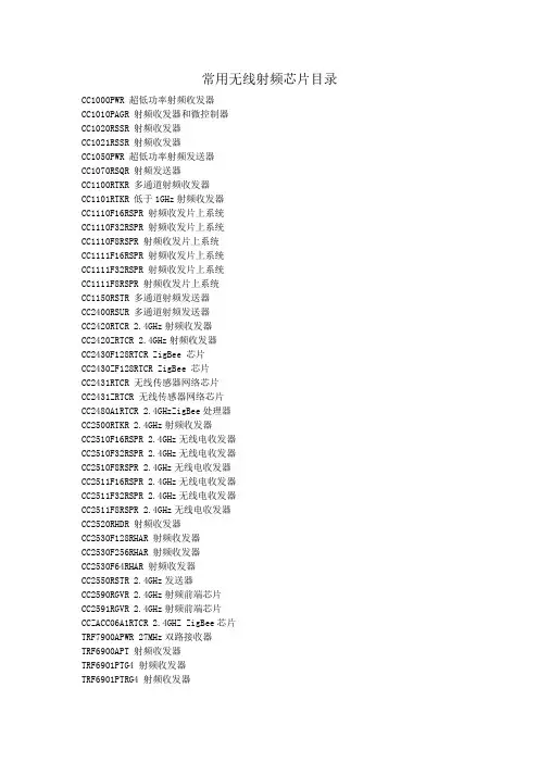
常用无线射频芯片目录CC1000PWR 超低功率射频收发器CC1010PAGR 射频收发器和微控制器CC1020RSSR 射频收发器CC1021RSSR 射频收发器CC1050PWR 超低功率射频发送器CC1070RSQR 射频发送器CC1100RTKR 多通道射频收发器CC1101RTKR 低于1GHz射频收发器CC1110F16RSPR 射频收发片上系统CC1110F32RSPR 射频收发片上系统CC1110F8RSPR 射频收发片上系统CC1111F16RSPR 射频收发片上系统CC1111F32RSPR 射频收发片上系统CC1111F8RSPR 射频收发片上系统CC1150RSTR 多通道射频发送器CC2400RSUR 多通道射频发送器CC2420RTCR 2.4GHz射频收发器CC2420ZRTCR 2.4GHz射频收发器CC2430F128RTCR ZigBee 芯片CC2430ZF128RTCR ZigBee 芯片CC2431RTCR 无线传感器网络芯片CC2431ZRTCR 无线传感器网络芯片CC2480A1RTCR 2.4GHzZigBee处理器CC2500RTKR 2.4GHz射频收发器CC2510F16RSPR 2.4GHz无线电收发器CC2510F32RSPR 2.4GHz无线电收发器CC2510F8RSPR 2.4GHz无线电收发器CC2511F16RSPR 2.4GHz无线电收发器CC2511F32RSPR 2.4GHz无线电收发器CC2511F8RSPR 2.4GHz无线电收发器CC2520RHDR 射频收发器CC2530F128RHAR 射频收发器CC2530F256RHAR 射频收发器CC2530F64RHAR 射频收发器CC2550RSTR 2.4GHz发送器CC2590RGVR 2.4GHz射频前端芯片CC2591RGVR 2.4GHz射频前端芯片CCZACC06A1RTCR 2.4GHZ ZigBee芯片TRF7900APWR 27MHz双路接收器TRF6900APT 射频收发器TRF6901PTG4 射频收发器TRF6901PTRG4 射频收发器TRF6903PTG4 射频收发器TRF6903PTRG4 射频收发器ADF7020-1BCPZ-RL7 射频收发IC ADF7020BCPZ-RL7 射频收发ICADF7021BCPZ-RL7 ISM无线收发IC ADF7021-NBCPZ-RL7 ISM无线收发IC ADF7025BCPZ-RL7 射频收发ICADF7010BRUZ-REEL7 ISM无线发射IC ADF7011BRUZ-RL7 ISM无线发射IC ADF7012BRUZ-RL7 UHF无线发射IC ADF7901BRUZ-RL7 ISM无线发射IC A7121A71C21AQF 2.4GHz射频收发器A7122A71C22AQF 2.4GHz射频收发器A7102A71C02AQF 射频收发ICA7103A71C03AUF 射频收发ICA7201A72C01AUF 射频接收ICA7202A72C02AUF 射频接收ICA7302A73C02AMF 射频发射ICA7105A71X05AQF 2.4GHz射频收发IC A7125A71X25AQF 2.4GHz射频收发IC A7325A73X25AQF 2.4GHz射频发射IC A7303AA73C03AQF FM发射芯片A7303AA73C03AUF FM发射芯片A7303BA73C03BUF FM发射芯片A7303BA73C03BQF FM发射芯片A7282A72N82AQF GPS接收芯片A7531BA75C31BQF GPS开关芯片A7532A75C32AQF GPS开关芯片A7533A75X33AQF GPS开关芯片A7533A75X33BQF GPS开关芯片AS3931 低功耗无线接收芯片AS3932BTSW 低功耗无线接收芯片AS3932BQFW 低功耗无线接收芯片AS3977BQFT FSK发射芯片AT86RF211DAI-R 射频收发ICAT86RF211SAHW-R 射频收发ICAT86RF212-ZU 射频收发ICAT86RF230-ZU 射频收发ICAT86RF231-ZU 射频收发ICATA2745M-TCQY 射频发送ICATA5428-PLQW 宽带收发ICATR2406-PNQG 2.4GHz射频收发IC T5750-6AQ 无线发射ICT5753-6AQ 无线发射ICT5754-6AQ 无线发射ICT7024-PGPM 前端收发器U2741B-NFB 无线发射ICAX5051 射频收发器ICAX5042 射频收发器ICAX5031 射频收发器ICAX50424 射频收发器ICAX6042 射频收发器ICCYRF6936-40LFXC 无线USB芯片CYRF7936-40LFXC 无线收发器芯片CYWUSB6932-28SEC 无线USB芯片CYWUSB6934-28SEC 无线USB芯片CYWUSB6934-48LFXC 无线USB芯片CYWUSB6935-28SEI 无线USB芯片CYWUSB6935-48LFI 无线USB芯片CYWUSB6935-48LFXC 无线USB芯片CYWUSB6935-48LFXI 无线USB芯片CYRF69103-40LFXC 无线射频芯片CYRF69213-40LFXC 无线射频芯片CYWUSB6953-48LFXC 无线USB芯片EM2420-RTR ZigBee 芯片EM260-RTR ZigBee 芯片EM250-RTR ZigBee 芯片EM351-RTR ZigBee 芯片EM357-RTR ZigBee 芯片PA5305 射频功率放大器PA2420 射频功率放大器PA2421 射频功率放大器PA2432 射频功率放大器FM2422 射频前端模块FM2422U 射频前端模块FM2427 射频前端模块FM2429 射频前端模块FM2429U 射频前端模块FM2446 射频前端模块FM7705 射频前端模块FM7707 射频前端模块MC13190FCR2 射频收发ICMC13191FCR2 射频收发ICMC13192FCR2 射频收发ICMC13193FCR2 射频收发ICMC13201FCR2 射频收发ICMC13202FCR2 射频收发ICMC13203FCR2 射频收发ICMC13211R2 射频收发ICMC13212R2 射频收发ICMC13213R2 射频收发ICMC13214R2 射频收发ICMC13224V 802.15.4/ZigBee芯片TDA5200 ASK接收器TDA5201 ASK接收器TDA5210 ASK/FSK接收器TDA5211 ASK/FSK接收器TDA5212 ASK/FSK接收器TDA5220 ASK/FSK接收器TDA5221 ASK/FSK接收器TDA7200 ASK/FSK接收器TDA7210 ASK/FSK接收器TDA5230 ASK/FSK接收器TDA5231 ASK/FSK接收器TDK5100 ASK/FSK发射器TDK5100F ASK/FSK发射器TDK5101 ASK/FSK发射器TDK5101F ASK/FSK发射器TDK5102 ASK/FSK发射器TDK5103A ASK发射器TDK5110 ASK/FSK发射器TDK5110F ASK/FSK发射器TDK5111 ASK/FSK发射器TDK5111F ASK/FSK发射器TDA7116F ASK/FSK发射器PMA7105 ASK/FSK发射器PMA7106 ASK/FSK发射器PMA7107 ASK/FSK发射器PMA7110 ASK/FSK发射器TDA5250 ASK/FSK收发器TDA5251 ASK/FSK收发器TDA5252 ASK/FSK收发器TDA5255 ASK/FSK收发器MAX1470EUI+T 无线接收IC MAX1471ATJ+T 无线接收IC MAX1472AKA+T 无线发射IC MAX1473EUI+T 无线接收IC MAX1479ATE+T 无线发射IC MAX7030HATJ+T 无线收发IC MAX7030LATJ+T 无线收发IC MAX7031LATJ+T 无线收发IC MAX7031MATJ50+T 无线收发ICMAX7032ATJ+T 无线收发IC MAX7033ETJ+T 无线接收IC MAX7044AKA+T 无线发射IC MAX7058ATG+T 无线发射IC MLX71121ELQ 射频接收IC MLX71122ELQ 射频接收IC TH71071EDC 射频接收IC TH71072EDC 射频接收IC TH7107EFC 射频接收IC TH71081EDC 射频接收IC TH71082EDC 射频接收IC TH7108EFC 射频接收IC TH71101ENE 射频接收IC TH71102ENE 射频接收IC TH71111ENE 射频接收IC TH71112ENE 射频接收IC TH71221ELQ 射频接收IC TH7122ENE 射频收发IC TH72001KDC 射频发射IC TH72002KDC 射频发射IC TH72005KLD 射频发射IC TH72006KLD 射频发射IC TH72011KDC 射频发射IC TH72012KDC 射频发射IC TH72015KLD 射频发射IC TH72016KLD 射频发射IC TH72031KDC 射频发射IC TH72032KDC 射频发射IC TH72035KLD 射频发射IC TH72036KLD 射频发射IC MICRF102BM 无线发射IC MICRF112YMM 无线发射IC MICRF113YM6 无线发射IC MICRF302YML 射频编码器MICRF405YML 射频发射IC MICRF505BML 射频收发IC MICRF506BML 射频收发IC MICRF002YM 射频接收器MICRF005YM 无线接收IC MICRF007BM UHF接收器MICRF008BM 无线接收IC MICRF009BM UHF接收IC MICRF010BM UHF接收IC MICRF011BM 射频ICMICRF211AYQS 射频接收器MRF24J40-I/ML ZigBee芯片MRF24J40T-I/ML ZigBee芯片MCP2030-I/P 免钥登录芯片MCP2030-I/SL 免钥登录芯片MCP2030-I/ST 免钥登录芯片MCP2030T-I/SL 免钥登录芯片MCP2030T-I/ST 免钥登录芯片nRF2401AG 2.4GHz收发器IC nRF24AP1 2.4GHz收发器IC nRF24E1G 2.4GHz收发器IC nRF24E2G 2.4GHz发射器IC nRF24L01+ 2.4GHz收发器IC nRF24LE1 2.4GHz收发器IC nRF24LU1 2.4GHz收发器IC nRF24Z1 2.4GHz收发器ICNRF905 430 928MHz收发器NRF9E5 430-928MHz收发器MFRC50001T/0FE,112 阅读器IC MFRC53001T/0FE,112 阅读器IC MFRC53101T/0FE,112 阅读器IC MFRC52301HN1 阅读器ICPN5110A0HN1/C2 收发器ICPN5120A0HN1/C1 收发器ICPN5310A3HN/C203 NFC控制器IC PN1000 GPS RF接收ICRX3400 射频接收ICRX3930 射频接收ICRX3140 射频接收ICRX3310A 射频接收ICRX3361 射频接收ICRX3408 射频接收ICPT4301 射频接收ICPT4316 射频接收ICPT4450 射频发射ICTX4915 射频发射ICTX4930 射频发射ICPA2460 功率放大器ICPA2464 功率放大器ICFS8107E 锁相环ICFS8108 锁相环ICFS8160 锁相环ICFS8170 锁相环ICFS8308 锁相环ICMG2400-F48 ZigBee单芯片MG2450-B72 ZigBee单芯片MG2455-F48 ZigBee单芯片AP1092 功率放大器ICAP1098 功率放大器ICAP1110 功率放大器ICAP1091 功率放大器ICAP1093 功率放大器ICAP1280 PA/LNA功率放大器AP1213 射频前端模块AP1290 功率放大器ICAP1291 功率放大器ICAP1294 功率放大器ICAP1045 功率放大器ICAP1046 功率放大器ICAP2085 功率放大器ICAP2010C 功率放大器ICAP3011 功率放大器ICAP3013 功率放大器ICAP3014 功率放大器ICAP3015 功率放大器ICAP3211 功率放大器ICSX1211I084TRT 单芯片收发器SX1441I077TRLF 系统蓝牙芯片XE1203FI063TRLF 射频收发芯片XE1205I074TRLF 射频收发芯片XE1283I076TRLF 射频收发芯片XM1203FC433XE1 射频收发芯片XM1203FC868XE1 射频收发芯片XM1203FC915XE1 射频收发芯片SX1223I073TRT 射频发射芯片SI3400-E1-GM 以太网电源ICSI3401-E1-GM 以太网电源ICSI3460-D01-GM 以太网电源ICSI4020-I1-FT 射频发射ICSI4021-A1-FT 射频发射ICSI4022-A1-FT 射频发射ICSI4030-A0-FM 射频发射ICSI4031-A0-FM 射频发射ICSI4032-V2-FM 射频发射ICSi4230-A0-FMIA4230 无线发射IC Si4231-A0-FMIA4231 无线发射IC Si4232-A0-FMIA4232 无线发射IC Si4320-J1-FT 无线接收ICSi4322-A1-FT 无线接收ICSi4330-V2-FMIA4330 无线接收IC SI4420-D1-FT 射频收发ICSI4421-A1-FTIA4421 无线收发IC SI4430-A0-FMIA4430 无线收发IC SI4431-A0-FMIA4431 无线收发IC SI4432-V2-FMIA4432 无线收发IC TM1001 功率放大器ICTM1006 功率放大器ICTM1008 射频晶体管TM3001 射频开关ICTM3002 射频开关ICTM4001 FM发射ICUW2453 无线网络ICUZ2400 ZigBee 芯片UP2206 2.4GHz功率放大器UP2268 2.4GHz功率放大器UA2707 射频信号放大器UA2709 射频信号放大器UA2711 射频信号放大器UA2712 射频信号放大器UA2715 射频信号放大器UA2716 射频信号放大器UA2725 射频信号放大器UA2731 射频信号放大器UA2732 射频信号放大器W2805 无线视频ICW2801 无线音频IC。
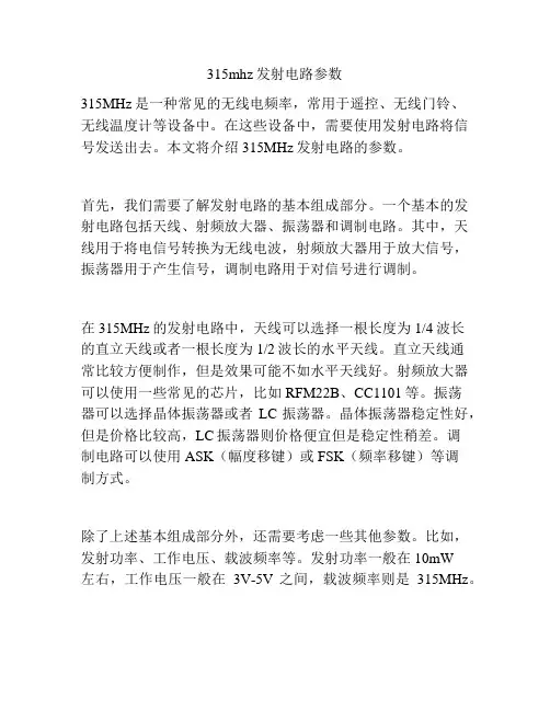
315mhz发射电路参数
315MHz是一种常见的无线电频率,常用于遥控、无线门铃、
无线温度计等设备中。
在这些设备中,需要使用发射电路将信号发送出去。
本文将介绍315MHz发射电路的参数。
首先,我们需要了解发射电路的基本组成部分。
一个基本的发射电路包括天线、射频放大器、振荡器和调制电路。
其中,天线用于将电信号转换为无线电波,射频放大器用于放大信号,振荡器用于产生信号,调制电路用于对信号进行调制。
在315MHz的发射电路中,天线可以选择一根长度为1/4波长
的直立天线或者一根长度为1/2波长的水平天线。
直立天线通
常比较方便制作,但是效果可能不如水平天线好。
射频放大器可以使用一些常见的芯片,比如RFM22B、CC1101等。
振荡
器可以选择晶体振荡器或者LC振荡器。
晶体振荡器稳定性好,但是价格比较高,LC振荡器则价格便宜但是稳定性稍差。
调
制电路可以使用ASK(幅度移键)或FSK(频率移键)等调
制方式。
除了上述基本组成部分外,还需要考虑一些其他参数。
比如,发射功率、工作电压、载波频率等。
发射功率一般在10mW
左右,工作电压一般在3V-5V之间,载波频率则是315MHz。
总之,315MHz发射电路的参数包括天线、射频放大器、振荡器、调制电路、发射功率、工作电压、载波频率等。
在实际应用中,需要根据具体情况进行选择和调整。
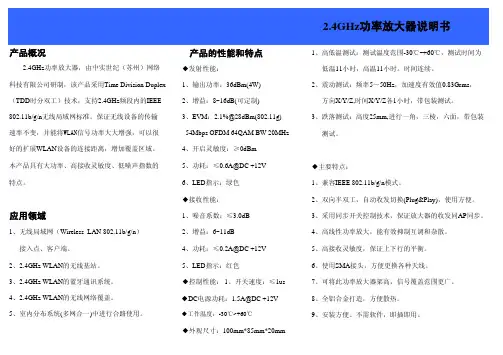
产品的性能和特点1、高低温测试:测试温度范围-30℃~+60℃,测试时间为 ◆发射性能:低温11小时,高温11小时。
时间连续。
1、输出功率:36dBm(4W)2、震动测试:频率5~50Hz ,加速度有效值0.83Grms , 2、增益:8~16dB(可定制) 方向X/Y/Z,时间X/Y/Z 各1小时,带包装测试。
3、EVM :2.1%@28dBm(802.11g) 3、跌落测试:高度25mm,进行一角,三棱,六面,带包装 54Mbps OFDM 64QAM BW 20MHz 测试。
4、开启灵敏度:≥0dBm5、功耗:≤0.6A@DC +12V ◆主要特点:6、LED 指示:绿色 1、兼容IEEE 802.11b/g/n 模式。
◆接收性能:2、双向半双工,自动收发切换(Plug&Play),使用方便。
1、噪音系数:≤3.0dB3、采用同步开关控制技术,保证放大器的收发同AP 同步。
2、增益:6~11dB4、高线性功率放大,能有效抑制互调和杂散。
4、功耗:≤0.2A@DC +12V5、高接收灵敏度,保证上下行的平衡。
5、LED 指示:红色6、使用SMA 接头,方便更换各种天线。
◆控制性能: 1、开关速度:≤1us7、可将此功率放大器架高,信号覆盖范围更广。
◆DC 电源功耗:1.5A@DC +12V 8、全铝合金打造,方便散热。
◆工作温度:-30℃~+60℃9、安装方便、不需软件,即插即用。
◆外观尺寸:100mm*85mm*20mm2.4GHz 功率放大器说明书产品概况应用领域好的扩展WLAN 设备的连接距离,增加覆盖区域。
本产品具有大功率、高接收灵敏度、低噪声指数的特点。
1、无线局域网(Wireless LAN 802.11b/g/n ) 接入点、客户端。
2、2.4GHz WLAN 的无线基站。
3、2.4GHz WLAN 的蓝牙通讯系统。
4、2.4GHz WLAN 的无线网络覆盖。
电子信息对抗技术Electronic Information Warfare Technology2019,34(2) 中图分类号:TN722.75 文献标志码:A 文章编号:1674-2230(2019)02-0068-05收稿日期:2018-07-06;修回日期:2018-08-06作者简介:闫磊(1981 ),男,硕士,工程师;蒋超(1983 ),男,硕士,工程师㊂VHF /UHF 频段1kW 功率放大器设计闫 磊,蒋 超(电子信息控制重点实验室,成都610036)摘要:设计了一种基于功率合成方式的功率放大器,工作于100~500MHz 频段范围㊂模块内部采用4个功放管合成的方式,实现了宽频带1kW 的功率输出;内部通过多级放大的方式,获得了较高的增益和较小的带内波动㊂针对VHF /UHF 频段特点,选择了大功率LDMOS 器件,采用基于传输线变压器的匹配电路和功率分配/合成方式,使最终效率达到40%以上㊂关键词:功率放大器;传输线变压器;功率合成;LDMOS DOI :10.3969/j.issn.1674-2230.2019.02.016Design of VHF /UHF Band 1kW Power AmplifierYAN Lei,JIANG Chao(Science and Technology on Electronic Information Control Laboratory,Chengdu 610036,China)Abstract :Based on power combining technology,A power amplifier is designed to work in100~500MHz bandwidth.This amplifier can deliver over 1kW output power in VHF /UHF broadband by using 4power transistors.It’s a multi-stage amplifier,which has a very high gain and low flatness.According to the characteristics of VHF /UHF band,high power LDMOS tran⁃sistors are used in amplify circuit.Meanwhile transmission line transformer is used in matchingcircuit and splitter /combiner.The efficiency is over 40%.Key words :power amplifier;transmission line transformer;power combining;LDMOS 1 引言无论是移动通信领域,还是电子对抗或干扰领域,功率放大器都起着十分重要的作用,往往是整个系统中最昂贵的部分,也是最容易损坏的部分㊂功率放大器的可靠性是影响整个系统正常工作的关键因素,且不同应用领域也对功率放大器的指标提出了不同的要求㊂无线通信领域要求功率放大器有很高的线性度,这是因为信号的幅度和相位都携带信息;干扰领域则需要功率放大器有较高的输出功率[1]㊂为了提高功放的输出功率,一般通过选择更大输出功率的器件和功率合成两种方式实现㊂器件的输出功率越大,意味着发热量越大,散热设计越困难,可靠性也随之降低,同时也造成与器件相关的匹配电路和供电电路的发热量变大,设计中需考虑更多器件的发热量和散热措施㊂另外,器件的输出功率与工作频带宽度成反比,宽带应用也限制了大功率器件的选择㊂为了解决这些问题,在大功率功放设计时,通常选择功率合成的方式,这样可降低每个器件的输出功率从而简化设计㊂但功率合成器会带来额外损耗,特别是当合成路数变多时损耗会显著增大,从而降低整体效率;同时合成路数过多也会带来电路体积的增加㊂因此设计中会综合考虑功率㊁体积㊁散热条件等因素,根据实际情况选择合适的器件和相应的合成方式㊂本文在设计功放86电子信息对抗技术·第34卷2019年3月第2期闫 磊,蒋 超VHF /UHF 频段1kW 功率放大器设计时,先确定合成方式,再选择功率器件,最终实现1kW 输出目标㊂2摇功放设计 经过多年的发展,射频功率器件已相当成熟,特别是近年来宽禁带半导体GaN HEMT 器件更是引发了各种应用热点,因其宽频带㊁高效率㊁高功率密度的特点在各领域得到了广泛应用㊂在VHF-UHF 频段低端,由于频段低,GaN HEMT 器件的优势无法体现,相反其热阻大㊁成本高的缺点制约了其应用㊂因此在设计中仍然首选传统的LDMOS 功率器件[2]㊂本文实际设计带宽是100MHz ~500MHz,此频段的功率分配/合成器多以同轴电缆传输线变压器的形式为主,根据1kW 的输出要求,选择4路合成方式,每1路功率在300W 左右,即能保证器件散热,又能保证合成效率㊂为了选择合适的功率器件,对此频段内两种典型大功率器件进行了比较㊂表1 器件参数比较BLF574MRFE6VP5600H供电电压50V 50V 最高工作频率500MHz 600MHz 测试频点225MHz 230MHz 输出功率500W 600W 增益26.5dB 24.6dB 最佳源阻抗(3.2+j2.5)Ω(1.8+j5.5)Ω最佳负载阻抗(7.5+j4.0)Ω(2.8+j5.3)Ω从器件厂商提供的数据看,两个器件都满足要求,通过适当降低工作电压,可将输出功率调节在合适的范围㊂因此必须从其它数据判断㊂选择功放管的一个重要指标是看其输入输出阻抗,特别是输出阻抗,其影响器件的输出功率㊁带宽和效率㊂输出阻抗中的电阻部分可粗略计算[3]:R out =(V cc -V sat )22P out (BJT 器件)或R out =(V dd -V ds(on))22P out (FET 器件ìîíïïïïï)(1)通常计算时V sat 或V ds(on)可忽略,而此次选择的都是推挽放大的LDMOSFET 器件,其输出电阻为:R out =2(V dd -V ds(on))2P out(2)根据(2)式,BLF574的输出电阻为2×502/500=10Ω,MRFE6VP5600H 的输出电阻为2×502/600=8.3Ω㊂而根据表1,BLF574的最佳负载阻抗为7.5+j4,MRFE6VP5600H 的最佳负载阻抗为2.8+j5.3,对比可知MRFE6VP5600H 的输出电阻较小,与计算值相差较大,说明其输出Q 值高,很难实现宽带匹配,相反,BLF574的输出电阻与理论值较接近,因此最终选择BLF574㊂图1 100MHz 负载LoadPull 仿真结果器件模型是双管形式,图1对其中单管进行了LoadPull 仿真,得到100MHz 的等功率和等效率曲线㊂一般情况下,输出功率最优和效率最优会给出两个不同的负载阻抗,实际设计中会根据需要选择合适的负载阻抗以满足对输出功率和效率的要求㊂表2 不同频点负载阻抗LoadPull 结果效率最优输出功率最优100MHz 11.6+j16 6.8+j8.6200MHz 6.8+j98.4+j3.4300MHz 6.8+j8.8 3.2+j3.2400MHz 1.2+j7.8 3.0+j3.2500MHz3.8+j1.6 3.8+j1.496闫 磊,蒋 超VHF /UHF 频段1kW 功率放大器设计投稿邮箱:dzxxdkjs@为了将表2中器件输入输出阻抗匹配到50Ω,在低于500MHz 频段的宽带应用中,应采用基于同轴电缆结合磁芯的传输线变压器形式㊂完整电路如图2所示㊂由于BLF574是双管形式,输入端先使用1:1不平衡-平衡变换器(balun),将输入信号转换成差分信号,此变换器由1根穿过磁芯的50Ω同轴电缆构成;与输入端相对应,输出端同样采用1:1平衡-不平衡变换器,将差分信号转换成单端信号,不同的是没有使用磁芯,因为输出端功率较大,使用磁芯会带来损耗并降低效率㊂设R g 表示源阻抗,R b 表示负载阻抗,n 2表示阻抗变换比,三者的关系是:R b =n 2R g ㊂(3)使用同轴电缆传输线变压器构成的阻抗变换器,实际应用中阻抗比n 2常取2.25㊁4㊁9㊁16这几个值,其它形式的阻抗变换电路,由于受到电路复杂度以及损耗等因素的限制,在功放匹配电路中应用较少㊂设同轴电缆特性阻抗为Z 0,对于大多数理想的阻抗变换器,R b ㊁R g ㊁Z 0三者的关系为[4]:Z 0=R b R g =R b /n(4)从表1可知,BLF574的源阻抗比负载阻抗更低,因此输入和输出匹配电路分别使用9:1和4:1的阻抗变换器,理想情况下根据(4)式应分别选择16.6Ω和25Ω的同轴电缆,而实际中为兼顾各频点的功率和效率,最终电缆阻抗分别调整为10Ω和15Ω㊂构成阻抗变换器的同轴电缆没有使用磁芯,这是因为磁芯会带来额外损耗,且不能明显提升电路性能㊂同轴电缆的长度通常<λmin /8,λmin是最短工作波长,即最高工作频点对应的波长㊂图2 BLF574电路图为了缩小功率分配/合成器的体积,其同样使用同轴电缆传输线变压器构成㊂功率分配器的电路结构与合成器相同,由于通过功率较小,可降低每个器件的功率容量,有利于电路的小型化㊂4合1功率合成器本质上由两级2合1功率合成器组成㊂图3是一种常见的功率合成器电路形式[5],具有低插损㊁高隔离㊁小体积等优点,可实现输入输出全50Ω匹配㊂同轴电缆T1和T2穿过磁芯构成一组2合1的功率合成器,R1是隔离电阻,合成器输出阻抗为25Ω㊂T3㊁T4㊁R2组成另一组完全相同的合成器,4路信号经两组合成器后变为两路信号㊂T5㊁T6㊁R3组成的电路起到增加隔离度的作用,将两路信号进行隔离后送入由T7㊁T8㊁R4组成的合成电路㊂最终的合成电路与之前不同在于,其输入阻抗是25Ω,而输出阻抗是50Ω,因此电路形式也不同㊂实际调试中需调节各同轴电缆长度,同时通过调节电容容值和位置来调节每路的插损和驻波比㊂图3 功率分配/合成器电路图为了提高整个功放的增益,内部采用多级放大的方式㊂推动级同样采用功率合成的方式实现,如图4所示,目的是改善推动级的输入输出驻波比,优化级间匹配,减小增益波动㊂推动级的功率分配/合成器使用电桥IPP2092,将输入输出驻波比降低到1.5以下,从而使推动级和末级级联时,增益不产生明显波动㊂根据图7中的测试结果,末级最小增益在16~17dB,因此推动级输出功率至少需要25W㊂推动级功放管选择中功率器件MRFE6VS25L,输出功率为25W,合成后输出50W 功率㊂其输入输出分别使用4∶1和2.25∶1的宽带匹配电路㊂7电子信息对抗技术·第34卷2019年3月第2期闫 磊,蒋 超VHF /UHF 频段1kW功率放大器设计图4 推动级放大器电路图为了改善功放的增益平坦度,在功放输入端还配有均衡器㊂均衡器由LCR 元器件组成,通过谐振网络对增益进行补偿,将功放的整体增益波动降低到1dB 以内㊂图5是两种常用的均衡电路及其均衡效果㊂整个功放的功能框图如图6所示,由均衡器㊁推动级㊁末级三部分组成,各部分组成原理如前所述㊂由于均衡器和推动级的工作电流较小,整个功放的效率主要由末级决定㊂图5 均衡器电路图图6 整个功放组成框图3摇仿真和测试结果 以图2中的电路图为基础,在Rogers4350基材上使用Micro -Coax 公司同轴电缆制作出功放电路,并对其进行功率和效率测试,同时为了对比,在ADS 软件中对BLF574电路进行建模仿真,得到了不同频点输出300W 时的增益和效率曲线㊂图7 不同频点输出300W时的增益图8 不同频点输出300W 时的效率从图中可以看出,仿真与实测数据所处区间基本一致,说明器件模型具有一定的准确性,可用于指导实际设计调试㊂仿真的增益比实际偏高,两者差别随频率提高而增大;仿真效率与实际效率虽都在50%以上,但某些频点相对误差达到10%㊂这些数据说明器件模型与实际仍有差异,特别是功放管和同轴电缆的模型与实际相差较大,无法精确模拟实际器件㊂因此实际调试中需在设计基础上不断调整各器件的参数以达到所需结果㊂图9 功率合成器各端口驻波比17闫 磊,蒋 超VHF /UHF 频段1kW 功率放大器设计投稿邮箱:dzxxdkjs@126.com图10 功率合成器插损由于同轴电缆具有空间结构,特别是传输线变压器中磁芯的使用,给建模带来新的困难,因此功率合成器的设计一般在成熟电路基础上根据特定频段进行调试,以达到最终要求㊂使用Micro-Coax 同轴电缆,基于图3中的电路,并结合实际调试,其结果满足合成要求㊂如图9和图10所示,合成器每路插损小于0.6dB,保证了合成效率在90%左右㊂4个输入端口驻波比小于1.2,保证了4个BLF574功放管的输出功率和效率基本不变㊂如图6所示,将4个由BLF574为核心的功放电路㊁功率分配/合成器㊁推动级放大器㊁均衡器组合在一起进行调试,使用均衡器对推动级和末级的增益波动进行补偿,使最终增益平坦度在1dB 以内㊂等激励功率输入时,各频点输出功率和效率如图11所示㊂图11 最终输出功率和效率可以看出,最终合成效率比计算的低一些,这是由于功率合成器4个输入端口的驻波比略大于1,造成BLF574的工作效率与单独测试比略有下降,但仍可保证整体效率在40%以上㊂合成器输出驻波比偏大,但不影响合成效率㊂图12 实物照片4摇结束语 本文使用大功率LDMOS 器件,实现了VHF-UHF 频带内的宽带输出,同时借助功率合成的手段,实现了1kW 大功率输出㊂从设计过程可以看出,此频段内仿真手段起辅助作用,指标的提高主要通过调试获得㊂同时,功率合成器的使用会造成器件工作状态的变化从而导致效率降低㊂因此,在进行功率合成器设计时,为了提高合成效率,除降低插损外,更重要的是改善各输入端口的驻波比㊂参考文献:[1] 钟慧,程建,方正.机载大功率通信干扰系统运用研究[J].空军军事学术,2016(5):46-48.[2] 黄江,王卫华.新型的功率器件 射频LDMOS[J].微波学报,2006,22(3):48-51.[3] DYE N,GRANBERG H.Radio Frequency TransistorsPrinciples and Practical Applications[M].USA:Ne⁃wnes,2001:125.[4] 张纪钢.射频铁氧体宽带器件[M].北京:科学出版社,1986:81.[5] GrebennikovA.射频与微波放大器设计[M].张玉兴,译.北京:电子工业出版社,2006:127.欢迎投稿 欢迎订阅27。
LOW COST 1000 WATT, 300 VOLT RF POWERAMPLIFIER FOR 13.56 MHzPresented at RF EXPO EAST 1995A P P L I C A T I O N N O TELow Cost 1000 Watt, 300 Volt RF Power Amplifier for13.56MHzKenneth Dierberger Lee B. MaxApplications Engineering Manager Independent ConsultantAdvanced Power Technology Inc.6284 Squiredell Dr.405 SW Columbia St.San Jose, California 95129 USABend, Oregon 97702 USABobby McDonaldUNI-WEST ENGINEERING6329 Bethel Island Rd.Bethel Island, CA 94511 USAABSTRACTThis paper details the design, development , assembly and performance of a low cost, high-efficiency, 1000Watt, 13.56MHz RF power amplifier (PA) operated from a 300VDC supply, with an efficiency of 80%. The PA is built around a “symmetric Pair” of low cost RF power MOSFETs from Advanced Power Technology (APT). The transistors are from a new generation of high quality, commercial, HF/ VHF, silicon, 900V RF power MOSFETs in TO-247 packages. The paper addresses both the theoretical design and physical construction of the amplifier. The paper also contains a technical description of the RF power transistors.INTRODUCTIONMost transistorized RF Power Amplifiers operate from a DC to DC converter. This supply is usually low voltage, about 50V, and requires a down regulator when operated from AC mains. This converter is a significant portion of the overall cost of the RF amplifier system.As a result of IEC555-2, all electronic equipment sold in Europe with a power draw of greater than 250W will require power factor correction (PFC). The addition of a PFC preregulator to the system could add 50 to 100% to the cost of the power supply portion. The requirement for PFC is soon to follow in the USA and the rest of the world.The use of a new high voltage RF MOSFETs from Advanced Power Technology (APT) makes possible a new RF amplifier design which can be operated at 300V, allowing for the direct use of regulated output, thus eliminating the DC to DC converter, reducing the cost of the RF amplifier system.The new devices, like their predecessors, utilize the high performance of APT’s Power MOS IV® technology and the “symmetric pair”package.AMPLIFIER DESCRIPTIONThe amplifier is a 1000 Watt, 13.56MHz design operating in class C with a 300VDC power supply. Efficiency of the amplifier is 80 percent. The power amplifier is built around two “symmetric pair” of ARF444/ARF445 900V RF power MOSFETs provided in TO-247 plastic packages. The devices are electrically identical, except that they are packaged in “mirror image”pairs to facilitate a symmetrical layout that helps maintain the electrical symmetry required for push-pull operation. Figure 1 shows the circuit diagram of the amplifier, with the parts list given in Table 1. The amplifier is a classical push-pull configuration of a straight forward nature, using a simple L-C network for impedance matching and transformer-coupling to achieve the required complementary gate drive signals. A wideband wire wound transformer output circuit is used, with a conventional bifilar-wound RF choke for DC power supply isolation.Short, low inductance interconnections are easily made using the ARF444/ARF445 devices, because they can be mounted symmetrically in a common source configuration. In particular, the gate circuit should minimize inductance to avoid instability and losses when that inductance is combined with the high capacitance of the gates. Similarly, the frequency response of the output circuitry is improved with minimum stray inductance due to interconnections[1].The amplifier is operated directly from the PFC 300VDC power supply, eliminating the DC-DC converter, and is constructed on a heat sink sized for proper dissipation at the expected power levels. Figure 2 shows the component placement on the PC board and heat sink. The common source design of the package allows the device mounting to be accomplished without an insulator thus allowing good heat transfer to the heat sink with the use of thermal grease.INPUT NETWORKThe input network provides a 50Ω impedance to the driver source and transformation of the MOSFET gate impedance, as well as balanced drive for push-pull operation. The input network comprises capacitor C1, the input capacitance of the power MOSFETs and the series gate resistors, both transformed by T1. The proper selection of C1 tunes the input network for minimum input return loss at maximum power output [2].Transformer T1 provides a 9:1 impedance transformation of the MOSFET input impedance. It is constructed using two Fair-Rite cores #2643540002, µ=850 with 3 turns of strandedFigure 1. Circuit Diagram of the 1000 Watt Class C AmplifierPart Number DescriptionR1,R210Ω 1WR3-R18 4.7Ω 1WC1200pF Chip CapacitorsC2-C50.1µF Chip CapacitorsC6-C100.1µF Disk CeramicC11, C120.01 Disk CeramicQ1, Q3ARF444Q2, Q4ARF445L1, L2VK200-19/4BL3, L40.37µH: 6T, #18AWG, ID=0.438RFC12T, #14 PTFE coated twisted pair on a Fair-Rite #2643665702 shieldbead, µi=850T19:1(Z) conventional transformer; 3:1(T), #18 stranded PTFE coatedwire on two Fair-Rite #2643540002, µi=850T21:1(Z) conventional transformer; 2:2(T), #14 stranded PTFE coatedwire on two stacks of three Fair-Rite #2643102002 shielded bead, µi-850 BFC16T, #18 Twisted pair stranded PTFE coated wire on three stackedIndiana General Toroid #F624-19-Q1, µi=125Table 1. Parts List for the 1000 Watt Power AmplifierPTFE coated #18 wire on the primary and 1 turn of stranded PTFE coated #18 wire on the secondary. The secondary is coupled through the DC blocking capacitors C1-C2 and C3-C4 and resistors R3 through R18 to the gates of the MOSFETs. The resistor-inductor combination R1-L1 and R2-L2 stabilize the push-pull amplifier at lower frequency and provide the MOSFETs with a DC ground reference to insure the gates do not float to a DC potential thus unbalancing the amplifier bias points. The parallel resistors R3-R6, R7-R10, R11-R14 and R15-R18 in series with the gates of the MOSFET, prevent high frequency oscillation common when paralleling MOSFETs [3].OUTPUT CIRCUITThe 300VDC power input is delivered through a balanced feed choke [4]. The choke is designedto create a zero DC magnetic bias in the core when both transistors draw the same average current.With the devices operating 180 degrees out of phase, the construction of the windings presents a high impedance at 13.56MHz to the drain of each MOSFET. The choke is constructed by winding 6 turns of #18 stranded PTFE coated twisted pair around three stacked Indiana General Toroids #F624-19-Q1, µi=125.The output of the power devices is coupled to the output transformer T2 through two 0.37 µH inductors. The transformer is a wideband 1:1conventional transformer. No output filtering was used in the test amplifier, which has the third harmonic 30db down and the second harmonic 55db below the 1000 watt output power level.The transformer is constructed by winding 2turns of #14 stranded PTFE coated wire for the primary and 2 turns of #14 stranded PTFE coated wire for the secondary around two stacks of three Fair-Rite #2643102002 shield beads, µi=850.PERFORMANCE MEASUREMENTS The amplifier was operated under two conditions. First the amplifier was driven with a 13.56MHz RF signal, modulated by a 1kHz square wave, at a 50% duty cycle, up to a peak power out of 1200W. Second the amplifier was driven with a 13.56HMz CW RF signal up to a continuous power out of 1000W. Due to the close correlation of the modulated data and the CW data, it was concluded that there is significant thermal margin from using four 300W devices at 1000W CW. Figures 3 through 6 show the performance data for this amplifier. Figure 3 is a plot of P in versus P out and Figure 4 shows gain versus P out . The curves show the classical class C characteristics,with a low gain at low power output, improving as the output power increases. The gain peaks at 16.9db when the amplifier output is 800W, with a roll-off to 15.9db at 1200W.Efficiency versus P out is shown in Figure 5. As would be expected in class C, the efficiency is over 50% at power output above 300W. The efficiency rises to an outstanding 80.4% at 1000W,continuing upward to 84.4% at 1000W, continuing upward to 84.4% at 1200W output. Figure 6 is total amplifier power dissipation versus P out .Figure 3. Input Power versus Output PowerFigure 4. Gain versus Output PowerFigure 6. Total Amplifier Power Dissipation versus Output Power 300 VOLT POWER SUPPLYThe topology chosen for the 300 V olt PFC power supply is the commonly used continuous mode boost converter. This topology is the most popular where power requirements are greater than 750W. Figure 7 is a simplified schematic of the regulator which is implemented using an APT5012JNU2 and a Unitrode U3854 controller IC [5] [6] [7].The regulator operates by the controller sensing the rectified DC input and controlling the ON and OFF time of Q1 such that the current in L1 closely follows a sine wave which is in phase with the AC line voltage. During the OFF time of Q1, the inductor fly back transfers some of the stored energy in the inductor to the output storage capacitor. The controller senses the output voltage and adjusts the average current in the inductor such that the regulated voltage on the output capacitor is maintained at 300V.CONCLUSIONThis paper demonstrated a recent breakthrough in commercial solid state RF power device and circuit technology. The high quality, low cost, components and circuits described here, now make it possible to deliver solid state, 10,000 watt (or more), 13.56MHz power supplies costing less than an equivalent tube RF power supply.The combination of high voltage operation, high gain, and efficiency of 80 percent make this technology exciting just for performance alone. Combine that performance with component coststhat allow for multi-kilowatt, 13.56MHz amplifiers to be built at less than $0.25 per watt and you now have the first real breakthrough in commercial HF, RF power technology in over a decade.This is only the beginning. The commercial technology detailed in this paper will be evolving quickly into solid state devices and circuits for higher frequency, higher power, and even higher operating voltages.Figure 7. Simplified Circuit Diagram of the Power Factor Correction Power SupplyREFERENCES1.H.O. Granberg, "Good RF Construction Practices and Techniques," Motorola Application Note AR164, Motorola RF Device Data, V olume II, DL110 Rev 4.2.H.O. Granberg, "Broad Band Transformers and Power Combining Techniques for RF," Motorola Application Note AN749, Motorola RF Device Data, V olume II, DL110 Rev 4.3.Rudy Severns, et al, "Parallel Operation of Power MOSFETs" "Anomalous Oscillation and Turn-Off Behavior in a Vertical Power MOSFET," MOSPOWER Applications Handbook, Siliconix, Inc., 19844.William E. Sabin, Edgar O. Schoenike, et al, "Single Sideband Systems and Circuits," McGraw-Hill 19875.Phil Todd, "UC3854 Controlled Power Factor Correction Circuit Design", Unitrode Application Note U-134, Product and Applications Handbook 1993-946.Ken Dierberger, Denis Grafham, "Design ofa 3000 Watt Single MOSFET Power Factor Correction Circuit," APT Application Note APT9303.7.Ken Dierberger, Denis Grafham, "Customized ISOTOP® Module for High Power Boost Converters and Related Topologies," APT Application Note 9401.ISOTOP® is a registered trademark of SGS Thompson405 S.W. Columbia Street Bend, Oregon 97702 USA Phone: (503) 382-8028 Fax: (503) 388-0364Parc Cadera Nord - Av. Kennedy BAT B433700 Merignac, FrancePhone: 33-56 34 34 71Fax: 33-56 47 97 61Printed - August 1995。