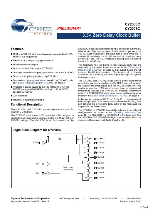
PRELIMINARYCY2305C CY2309C3.3V Zero Delay Clock BufferFeatures■10 MHz to 100-133 MHz operating range, compatible with CPU and PCI bus frequencies■Zero input and output propagation delay ■Multiple low skew outputs■One input drives five outputs (CY2305C)■One input drives nine outputs, grouped as 4 + 4 + 1 (CY2309C)■50 ps typical cycle-cycle jitter (15 pF, 66 MHz)■Test Mode to bypass phase locked loop (PLL) (CY2309C) only, see “Select Input Decoding for CY2309C” on page 3■Available in space saving 16-pin 150 Mil SOIC or 4.4 mm TSSOP packages (CY2309C), and 8-pin, 150 Mil SOIC package (CY2305C)■3.3V operation■Industrial temperature availableFunctional DescriptionThe CY2305C and CY2309C are die replacement parts for CY2305 and CY2309.The CY2309C is a low cost 3.3V zero delay buffer designed to distribute high speed clocks and is available in a 16-pin SOIC or TSSOP package. The CY2305C is an 8-pin version of theCY2309C. It accepts one reference input and drives out five low skew clocks. The -1H versions of each device operate up to 100-133 MHz frequencies and have higher drive than the -1devices. All parts have on-chip PLLs which lock to an input clock on the REF pin. The PLL feedback is on-chip and is obtained from the CLKOUT pad.The CY2309C has two banks of four outputs each that are controlled by the select inputs as shown in the “Select Input Decoding for CY2309C” on page 3. If all output clocks are not required, BankB is three-stated. The input clock is directly applied to the outputs by the select inputs for chip and system testing purposes.The CY2305C and CY2309C PLLs enter a power down mode when there are no rising edges on the REF input. In this state,the outputs are three-stated and the PLL is turned off. This results in less than 12.0 μA of current draw for commercial temperature devices and 25.0 μA for industrial temperature parts. The CY2309C PLL shuts down in one additional case as shown in the “Select Input Decoding for CY2309C” on page 3.In the special case when S2:S1 is 1:0, the PLL is bypassed and REF is output from DC to the maximum allowable frequency. The part behaves like a non-zero delay buffer in this mode and the outputs are not three-stated.The CY2305C or CY2309C is available in two or three different configurations as shown in the “Ordering Information” on page 11. The CY2305C-1 or CY2309C-1 is the base part. The CY2305-1H or CY2309-1H is the high drive version of the -1. Its rise and fall times are much faster than the -1s.Logic Block Diagram for CY2309CPLLMUXSelect Input REFS2S1CLKA1CLKA2CLKA3CLKA4CLKB1CLKB2CLKB3CLKB4DecodingCLKOUTPRELIMINARYCY2309CPRELIMINARYCY2309CPinoutsCY2309CTable 1. Pin Definition - 16 Pin SOIC/TSSOPFigure 1. Pin Diagram - 16 Pin SOIC/TSSOPPin SignalDescription1REF [1]Input reference frequency 2CLKA1[2]Buffered clock output, Bank A 3CLKA2[2]Buffered clock output, Bank A 4V DD 3.3V supply 5GND Ground6CLKB1[2]Buffered clock output, Bank B 7CLKB2[2]Buffered clock output, Bank B 8S2[3]Select input, bit 29S1[3]Select input, bit 110CLKB3[2]Buffered clock output, Bank B 11CLKB4[2]Buffered clock output, Bank B 12GND Ground 13V DD 3.3V supply14CLKA3[2]Buffered clock output, Bank A 15CLKA4[2]Buffered clock output, Bank A16CLKOUT [2]Buffered output, internal feedback on this pin12345678910111213141516REF CLKA1CLKA2V DD GND CLKB1CLKB2S2CLKOUT CLKA4CLKA3V DD GND CLKB4CLKB3S1SOIC/TSSOP Top ViewCY2309CNotes1.Weak pull down.2.Weak pull down on all outputs.3.Weak pull ups on these inputs.4.This output is driven and has an internal feedback for the PLL. The load on this output is adjusted to change the skew between the reference and output.Table 2. Select Input Decoding for CY2309CS2S1CLOCK A1–A4CLOCK B1–B4CLKOUT [4]Output SourcePLL Shutdown00Three state Three state Driven PLL N 01Driven Three state Driven PLL N 10Driven Driven Driven Reference Y 11DrivenDrivenDrivenPLLNPRELIMINARYCY2309CCY2305CZero Delay and Skew ControlAll outputs should be uniformly loaded to achieve Zero Delay between the input and output. Since the CLKOUT pin is the internal feedback to the PLL, its relative loading can adjust the input or output delay.For applications requiring zero input or output delay, all outputs including CLKOUT are equally loaded. Even if CLKOUT is not used,it must have a capacitive load equal to that on other outputs for obtaining zero input or output delay.For zero output or output skew, all outputs are loaded equally. For further information refer to the application note entitled “CY2305and CY2309 as PCI and SDRAM Buffers”.Figure 2. Pin Diagram - 8 Pin SOICTable 3. Pin Description - 8 Pin SOICPin SignalDescription1REF [1]Input reference frequency 2CLK2[2]Buffered clock output 3CLK1[2]Buffered clock output 4GND Ground5CLK3[2]Buffered clock output 6V DD 3.3V supply7CLK4[2]Buffered clock output8CLKOUT [2]Buffered clock output, internal feedback on this pin12345876REF CLK2CLK1GNDV DD CLKOUT CLK4CLK3SOIC Top ViewCY2305CPRELIMINARYCY2309CAbsolute Maximum ConditionsSupply Voltage to Ground Potential................–0.5V to +4.6V DC Input Voltage (Except REF) ............–0.5V to V DD + 0.5V DC Input Voltage REF...........................–0.5V to V DD + 0.5VStorage Temperature .................................–65°C to +150°C Junction Temperature................................................. 150°C Static Discharge Voltage(per MIL-STD-883, Method 3015)...........................> 2,000VOperating Conditions for CY2305CSXC-XX and CY2309CSXC-XXOperating Conditions table for CY2305CSXC-XX and CY2309CSXC-XX Commercial Temperature Devices.Parameter DescriptionMin Max Unit V DD Supply Voltage3.0 3.6V T A Operating Temperature (Ambient Temperature)070°C C L Load Capacitance, below 100 MHz30pF C L Load Capacitance, from 100 MHz to 133 MHz 10pF C IN Input Capacitance7pF t PUPower up time for all V DD s to reach minimum specified voltage (power ramps are monotonic)0.0550msElectrical Characteristics for CY2305CSXC-XX and CY2309CSXC-XXElectrical Characteristics table for CY2305CSXC-XX and CY2309CSXC-XX Commercial Temperature Devices.Parameter DescriptionTest Conditions Min Max Unit V IL Input LOW Voltage [5]–0.30.8V V IH Input HIGH Voltage [5] 2.0V DD + 0.3V I IL Input LOW Current V IN = 0V –50μA I IH Input HIGH Current V IN = V DD–100μA V OL Output LOW Voltage [6]I OL = 8 mA (–1)I OH = 12 mA (–1H)–0.4V V OHOutput HIGH Voltage [6]I OH = –8 mA (–1)I OL = –12 mA (–1H) 2.4–V I DD (PD mode)Power Down Supply Current REF = 0 MHz–12.0μA I DDSupply CurrentUnloaded outputs at 66.67 MHz, SEL inputs at V DD–32mANotes5..REF input has a threshold voltage of V DD /2.6.Parameter is guaranteed by design and characterization. Not 100% tested in production.PRELIMINARY CY2309CSwitching Characteristics for CY2305CSXC-XX and CY2309CSXC-XXSwitching characteristics table for CY2305CSXC-1 and CY2309CSXC-1 Commercial Temperature Devices. All parameters are specified with loaded outputs.Parameter Name Test Conditions Min Typ Max Unitt1Output Frequency30 pF load10 pF load 1010–100133.33MHzMHzDuty Cycle[6] = t2÷ t1Measured at 1.4V, F out = 66.67 MHz40.050.060.0% t3Rise Time[6]Measured between 0.8V and 2.0V–– 2.25ns t4Fall Time[6]Measured between 0.8V and 2.0V–– 2.25ns t5Output to Output Skew[6]All outputs equally loaded––200ps t6A Delay, REF Rising Edge toCLKOUT Rising Edge[6]Measured at V DD/2–0±350pst6B Delay, REF Rising Edge toCLKOUT Rising Edge[6]Measured at V DD/2. Measured in PLLBypass Mode, CY2309C device only.158.7nst7Device to Device Skew[6]Measured at V DD/2 on the CLKOUT pinsof devices–0700pst J Cycle to Cycle Jitter, peak[6]Measured at 66.67 MHz, loaded outputs–50175pst LOCK PLL Lock Time[6]Stable power supply, valid clockpresented on REF pin–– 1.0msSwitching characteristics table for CY2305CSXC-1H and CY2309CSXC-1H Commercial Temperature Devices. All parameters are specified with loaded outputs.Parameter Name Description Min Typ Max Unitt1Output Frequency30-pF load10-pF load 1010–100133.33MHzMHzDuty Cycle[6] = t2÷ t1Measured at 1.4V, F out = 66.67 MHz40.050.060.0%Duty Cycle[6] = t2÷ t1Measured at 1.4V, F out < 50.0 MHz45.050.055.0% t3Rise Time[6]Measured between 0.8V and 2.0V–– 1.5ns t4Fall Time[6]Measured between 0.8V and 2.0V–– 1.5ns t5Output to Output Skew[6]All outputs equally loaded––200ps t6A Delay, REF Rising Edge toCLKOUT Rising Edge[6]Measured at V DD/2–0±350pst6B Delay, REF Rising Edge toCLKOUT Rising Edge[6]Measured at V DD/2. Measured in PLLBypass Mode, CY2309C device only.158.7nst7Device to Device Skew[6]Measured at V DD/2 on the CLKOUT pinsof devices–0700pst8Output Slew Rate[6]Measured between 0.8V and 2.0V usingTest Circuit #21––V/ns t J Cycle to Cycle Jitter, peak[6]Measured at 66.67 MHz, loaded outputs––175ps t LOCK PLL Lock Time[6]Stable power supply, valid clockpresented on REF pin–– 1.0msPRELIMINARY CY2309COperating Conditions for CY2305CSXI-XX and CY2309CSXI-XXOperating conditions table for CY2305CSXI-XX and CY2309CSXI-XX Industrial Temperature Devices.Parameter Description Min Max UnitV DD Supply Voltage 3.0 3.6VT A Operating Temperature (Ambient Temperature)–4085°CC L Load Capacitance, below 100 MHz–30pFC L Load Capacitance, from 100 MHz to 133 MHz–10pFC IN Input Capacitance–7pF Electrical Characteristics for CY2305CSXI-XX and CY2309CSXI-XXElectrical characteristics table for CY2305CSXI-XX and CY2309CSXI-XX Industrial Temperature Devices.Parameter Description Test Conditions Min Max UnitV IL Input LOW Voltage[5]–0.30.8VV IH Input HIGH Voltage[5] 2.0V DD + 0.3VI IL Input LOW Current V IN = 0V–50.0μAI IH Input HIGH Current V IN = V DD–100.0μA–0.4VV OL Output LOW Voltage[6]I OL = 8 mA (–1)I OH =12mA (–1H)2.4–VV OH Output HIGH Voltage[6]I OH = –8 mA (–1)I OL = –12 mA (–1H)I DD (PD mode)Power down Supply Current REF = 0 MHz–25.0μA–35mAI DD Supply Current Unloaded outputs at 66.67 MHz,SEL inputs at V DDPRELIMINARYCY2309CSwitching Characteristics for CY2305CSXI-XX and CY2309CSXI-XXSwitching characteristics table for CY2305CSXI-1and CY2309CSXI-1 Industrial Temperature Devices. All parameters are specified with loaded outputs.Parameter NameTest ConditionsMin TypMax Unit t 1Output Frequency 30 pF load 10 pF load1010100133.33MHz MHz Duty Cycle [6] = t 2 ÷ t 1Measured at 1.4V, F out = 66.67 MHz 40.050.060.0%t 3Rise Time [6]Measured between 0.8V and 2.0V –– 2.25ns t 4Fall Time [6]Measured between 0.8V and 2.0V –– 2.25ns t 5Output to Output Skew [6]All outputs equally loaded ––200ps t 6A Delay, REF Rising Edge to CLKOUT Rising Edge [6]Measured at V DD /2–0±350ps t 6BDelay, REF Rising Edge to CLKOUT Rising Edge [6]Measured at V DD /2. Measured in PLL Bypass Mode, CY2309C device only.158.7nst 7Device to Device Skew [6]Measured at V DD /2 on the CLKOUT pins of devices–0700ps t J Cycle to Cycle Jitter, peak [6]Measured at 66.67 MHz, loadedoutputs –50175ps t LOCKPLL Lock Time [6]Stable power supply, valid clock presented on REF pin––1.0msSwitching characteristics table for CY2305CSXI-1H and CY2309CSXI-1H Industrial Temperature Device. All parameters are specified with loaded outputs.Parameter NameDescriptionMin Typ Max Unit t 1Output Frequency 30 pF load 10 pF load1010–100133.33MHz MHz Duty Cycle [6] = t 2 ÷ t 1Measured at 1.4V, F out = 66.67 MHz 40.050.060.0%Duty Cycle [6] = t 2 ÷ t 1Measured at 1.4V, F out < 50.0 MHz 45.050.055.0%t 3Rise Time [6]Measured between 0.8V and 2.0V –– 1.5ns t 4Fall Time [6]Measured between 0.8V and 2.0V –– 1.5ns t 5Output to Output Skew [6]All outputs equally loaded––200ps t 6A Delay, REF Rising Edge to CLKOUT Rising Edge [6]Measured at V DD /2–0±350ps t 6BDelay, REF Rising Edge to CLKOUT Rising Edge [6]Measured at V DD /2. Measured in PLL Bypass Mode, CY2309C deviceonly.158.7nst 7Device to Device Skew [6]Measured at V DD /2 on the CLKOUT pins of devices–0700ps t 8Output Slew Rate [6]Measured between 0.8V and 2.0V using Test Circuit #21–V/nst J Cycle to Cycle Jitter, peak [6]Measured at 66.67 MHz, loadedoutputs ––175ps t LOCKPLL Lock Time [6]Stable power supply, valid clock presented on REF pin––1.0msPRELIMINARYCY2309CSwitching WaveformsFigure 3. Duty Cycle TimingFigure 4. All Outputs Rise/Fall TimeFigure 5. Output-Output SkewFigure 6. Input-Output Propagation DelayFigure 7. Device-Device Skewt 1t 21.4V1.4V1.4VOUTPUTt 33.3V 0V0.8V 2.0V 2.0V 0.8Vt 41.4V1.4Vt 5OUTPUTOUTPUTV DD /2t 6INPUTOUTPUTV DD /2V DD /2V DD /2t 7CLKOUT, Device 1CLKOUT, Device 2PRELIMINARYCY2309CTest Circuits0.1μFV DD0.1μFV DDCLKoutC LOADOUTPUTSGNDGND0.1μFV DD0.1μFV DD 10 pFOUTPUTSGNDGND1 k Ω1 k ΩTest Circuit # 1Test Circuit # 2For parameter t 8 (output slew rate) on -1H devicesPRELIMINARY CY2309COrdering InformationOrdering Code Package Type Operating RangePb-Free - CY2305CCY2305CSXC-18-pin 150 Mil SOIC CommercialCY2305CSXC-1T8-pin 150 Mil SOIC – Tape and Reel CommercialCY2305CSXC-1H8-pin 150 Mil SOIC CommercialCY2305CSXC-1HT8-pin 150 Mil SOIC – Tape and Reel CommercialCY2305CSXI-18-pin 150 Mil SOIC IndustrialCY2305CSXI-1T8-pin 150 Mil SOIC – Tape and Reel IndustrialCY2305CSXI-1H8-pin 150 Mil SOIC IndustrialCY2305CSXI-1HT8-pin 150 Mil SOIC – Tape and Reel IndustrialPb-Free- CY2309CCY2309CSXC-116-pin 150 Mil SOIC CommercialCY2309CSXC-1T16-pin 150 Mil SOIC – Tape and Reel CommercialCY2309CSXC-1H16-pin 150 Mil SOIC CommercialCY2309CSXC-1HT16-pin 150 Mil SOIC – Tape and Reel CommercialCY2309CSXI-116-pin 150 Mil SOIC IndustrialCY2309CSXI-1T16-pin 150 Mil SOIC – Tape and Reel IndustrialCY2309CSXI-1H16-pin 150 Mil SOIC IndustrialCY2309CSXI-1HT16-pin 150 Mil SOIC – Tape and Reel IndustrialCY2309CZXC-116-pin 4.4 mm TSSOP CommercialCY2309CZXC-1T16-pin 4.4 mm TSSOP – Tape and Reel CommercialCY2309CZXC-1H16-pin 4.4 mm TSSOP CommercialCY2309CZXC-1HT16-pin 4.4 mm TSSOP – Tape and Reel CommercialCY2309CZXI-116-pin 4.4 mm TSSOP IndustrialCY2309CZXI-1T16-pin 4.4 mm TSSOP – Tape and Reel IndustrialCY2309CZXI-1H16-pin 4.4 mm TSSOP IndustrialCY2309CZXI-1HT16-pin 4.4 mm TSSOP – Tape and Reel IndustrialPRELIMINARYCY2309CPackage Drawing and DimensionsFigure 9.16-Pin (150 Mil) SOIC S16PRELIMINARYCY2309CFigure 10.16-Pin TSSOP 4.40 MM Body Z16.173Document Number: 38-07672 Rev. *F Revised July 5, 2007Page 14 of 14PSoC Designer™, Programmable System-on-Chip™, and PSoC Express™ are trademarks and PSoC® is a registered trademark of Cypress Semiconductor Corp. All other trademarks or registered PRELIMINARYCY2305CCY2309C© Cypress Semiconductor Corporation, 2007. The information contained herein is subject to change without notice. Cypress Semiconductor Corporation assumes no responsibility for the use of any circuitry other than circuitry embodied in a Cypress product. Nor does it convey or imply any license under patent or other rights. Cypress products are not warranted nor intended to be used for medical,life support, life saving, critical control or safety applications, unless pursuant to an express written agreement with Cypress. Furthermore, Cypress does not authorize its products for use as critical components in life-support systems where a malfunction or failure may reasonably be expected to result in significant injury to the user. The inclusion of Cypress products in life-support systems application implies that the manufacturer assumes all risk of such use and in doing so indemnifies Cypress against all charges.Any Source Code (software and/or firmware) is owned by Cypress Semiconductor Corporation (Cypress) and is protected by and subject to worldwide patent protection (United States and foreign),United States copyright laws and international treaty provisions. Cypress hereby grants to licensee a personal, non-exclusive, non-transferable license to copy, use, modify, create derivative works of,and compile the Cypress Source Code and derivative works for the sole purpose of creating custom software and or firmware in support of licensee product to be used only in conjunction with a Cypress integrated circuit as specified in the applicable agreement. Any reproduction, modification, translation, compilation, or representation of this Source Code except as specified above is prohibited without the express written permission of Cypress.Disclaimer: CYPRESS MAKES NO WARRANTY OF ANY KIND, EXPRESS OR IMPLIED, WITH REGARD TO THIS MATERIAL, INCLUDING, BUT NOT LIMITED TO, THE IMPLIED WARRANTIES OF MERCHANTABILITY AND FITNESS FOR A PARTICULAR PURPOSE. Cypress reserves the right to make changes without further notice to the materials described herein. Cypress does not assume any liability arising out of the application or use of any product or circuit described herein. Cypress does not authorize its products for use as critical components in life-support systems where a malfunction or failure may reasonably be expected to result in significant injury to the user. The inclusion of Cypress’ product in a life-support systems application implies that the manufacturer assumes all risk of such use and in doing so indemnifies Cypress against all charges. Use may be limited by and subject to the applicable Cypress software license agreement.Document History PageDocument Title: CY2305C CY2309C 3.3V Zero Delay Clock Buffer Document Number: 38-07672REV.ECN NO.Issue Date Orig. of Change Description of Change**224421See ECN RGL New datasheet*A 268571See ECN RGL Added bullet for 5V tolerant inputs in the features*B 276453See ECN RGL Minor Change: Moved one sentence from the features to the Functional Description*C 303063See ECN RGL Updated datasheet as per characterization data *D 318315See ECN RGL Datasheet rewrite*E 344815See ECN RGL Minor Error: Corrected the header of all the AC/DC tables with the right part numbers.*F1279889See ECNKVMChanged title from “Low Cost 3.3V Zero Delay Buffer” to “3.3V Zero Delay Clock Buffer”Specified the VIL minimum value to -0.3VSpecified the VIH maximum value to VDD + 0.3VChanged DC Input Voltage (REF) maximum value in Absolute Maximum sectionRemoved references to 5V tolerant inputs (pages 1 and 2)Removed Pentium compatibility reference Added CY2305C block diagramAdded “peak” to the jitter specificationsChanged typical jitter from 75 ps to 50 ps for standard drive devicesFor standard drive devices, tightened rise/fall times from 2.5 ns to 2.25 ns Tightened cycle-to-cycle jitter from 200 ps to 175 ps Tightened output-to-output skew from 250 ps to 200 ps。