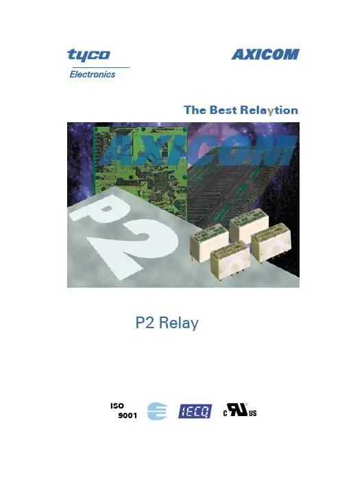
P2 RelayThe Best Rela ytion90012 pole telecom relay, polarized,Through Hole Type (THT) orSurface Mount Technology (SMT),Relay types: non-latching with 1 coil latching with 2 coils latching with 1 coilFeatures– Standard telecom relay (ringing and test access)– Slim line 15 x 7.5 mm, 0.590 x 0.295 inch – Switching current 5 A– 2 changeover contacts (2 form C / DPDT)– Bifurcated contacts – Immersion cleanable– High sensitivity results in low nominal power consumption 140 mW for non-latching and latching with 2 coils 70 mW for latching with 1 coil – For single coil version:- Surge voltage resistance between contact and coil for single coil version:- 2.5 kV (2 / 10 µsec) meets the Bellcore Requirement GR-1089 - 1.5 kV (10 / 160 µsec) meets FCC Part 68Typical applications– Communications equipmentlinecard application (ringing and test access) PABXVoice over IP – Office equipment– Measurement and control equipment – Automotive equipmentCAN bus, keyless entry, speaker switch – Medical equipment – Consumer electronics Set Top Boxes, HiFiOptions– 1500 Vrms between open contacts – Temperature range up to 105° CUL 508 File No. E111441UL 60950QC 160504-CH0003CECC 811-54-003Insulation category:Supplementary insulation according IEC / EN 60950Working voltage ³ 300 Vrms Mains supply voltage ³ 250 Vrms Repetitive peak voltage 2500 V Pollution degree: Internal: 1 External: 2Flammability classification: V-0Maximum operating temperature: 85 °CIEC/EN60950 IEC Ref. Cert. No. CH 2171DimensionsTHT THT SMT long terminals SMT long terminals SMT short terminals SMT short terminals V23079-x1xxx-B301 V23079-x2xxx-B301 V23079-x1xxx-B301 V23079-x2xxx-B301V23079-x1xxx-B301 V23079-x2xxx-B301 standard coil overmolded coil standard coil overmolded coil standard coil overmolded coilmm inch mm inch mm inch mm inch mm inch mm inchL 14.5 ± 0.1 0.570 ± 0.004 14.5 ± 0.1 0.570 ± 0.00414.5 ± 0.1 0.570 ± 0.00414.5 ± 0.10.570 ± 0.00414.5 ± 0.1 0.570 ± 0.00414.5 ± 0.10.570 ± 0.004 W 7.2 ± 0.1 0.283 ± 0.004 7.2 ± 0.1 0.283 ± 0.0047.2 -0.15 0.283 ± 0.0047.2 -0.15 0.283 ± 0.0047.2 -0.15 0.283 ± 0.0047.2 -0.15 0.283 ± 0.004 H9.8 ± 0.1 0.385 ± 0.004 9.5 ± 0.1 0.374 ± 0.00410.4 ± 0.15 0.409 ±0.006 9.9 ± 0.1 0.390 ± 0.00410.4 ± 0.150.409 ±0.006 9.9 ± 0.1 0.390 ± 0.004 T 3.25 - 0.25 0.128 -0.010 3.25 - 0.25 0.128 -0.010N/A N/A N/A N/A N/A N/A N/A N/AT1 N/A N/A N/A N/A 5.52 ±0.15 0.217 ±0.006 5.52 0.217 ±0.006 5.52 0.217 ±0.006 5.52 0.217 ±0.006 T2 N/A N/A N/A N/A 9.4 ±0.15 0.370 ±0.006 9.4 ±0.15 0.370 ±0.006 7.4 ±0.15 0.291 ±0.006 7.4 ±0.15 0.291 ±0.006 Tw0.5 ± 0.05 0.020 ±0.002 0.5 ± 0.05 0.020 ±0.0020.5 ± 0.05 0.020 ±0.002 0.5 ± 0.050.020 ±0.002 0.5 ± 0.05 0.020 ±0.002 0.5 ± 0.050.020 ±0.002 S 0.55 - 0.15 0.022 -0.0060.45 0.018 ±0.002N/A N/A N/A N/A N/A N/A N/A N/ATHT VersionNote: Hole for pin 6 and 7only for latching with 2 coilsBasic grid 2.54 mmLong terminalsSMT VersionShort terminalsNote: Solder pad for pin 6 and 7only for latching with 2 coilsNote: Solder pad for pin 6 and 7only for latching with 2 coilsLong terminals Short terminalsTerminal assignmentRelay - top viewLatching type, 2coilsreset condition Mounting hole layoutView onto the component side of the PCBSolder pad layoutView onto the component side of the PCBNon-latching type,not energized conditionLatching type, 1 coilreset conditionnon-latching 1 coilA1xxx/D1xxx/G1xxx A2xxx/D2xxx/G2xxx3 2.25 6.50 0.30 140 64.3 0084 3.00 8.70 0.40 140 114 016 4.5 3.375 9.80 0.45 140 145 011 5 3.75 10.90 0.50 140 178 0016 4.5 13.00 0.60 140 257 002 9 6.75 19.60 0.90 140 578 006 12 9.00 26.15 1.20 140 1029 003 24* 18.00 52.30 2.40 140 4114 005 3 2.25 6.50 2.25 140 64.3 208 4.5 3.375 9.80 3.375 140 145 211 5 3.75 10.90 3.75 140 178 201 6 4.5 13.00 4.50 140 257 202 9 6.75 19.60 6.75 140 578 206 12 9.00 26.15 9.00 140 1029 203 24 18.00 52.30 18.00 140 4114 205latching 2 coilslatching 1 coil3 2.25 9.20 2.25 70 128 108 4.5 3.375 13.85 3.375 70 289 111 5 3.75 15.33 3.75 70 357 101 6 4.5 18.50 4.50 70 514 102 9 6.75 27.75 6.75 70 1157 106 12 9.00 37.00 9.00 70 2057 103 24 18.00 74.00 18.00 70 8228 105* 24 V only in A1xxx/D1xxx/G1xxxFurther coil versions are available on request.Ambient temperature t amb [°C]B1xxx/E1xxx/H1xxxC1xxx/F1xxx/J1xxxU I = Minimum voltage at 23° C after pre-energizing with nominal voltage without contact current U II = Maximum continous voltage at 23°The operating voltage limits U I and U II depend on the temperature according to the formula:U I tamb = K I · U I 23° C and U II tamb = K Il · U Il 23° Ct amb = Ambient temperatureU I tamb = Minimum voltage at ambient temperature, t amb U II tamb = Maximum voltage at ambient temperature, t amb k I , k II = Factors (dependent on temperature), see diagramAll data refers to 23° C unless otherwise specified.Recommended soldering conditionsSoldering conditions according CECC 00802Vapor Phase Soldering: Temperature/Time Profile (Lead Temperature)Infrared Soldering: Temperature/Time Profile (Lead Temperature)Time (s)Time (s)T e m p e r a t u r e °CT e m p e r a t u r e °CTube for THT version - 50 relays per tube, 2000 relays per boxTape and reel for SMT version with long terminals - 400 relays per reel, 2000 relays per boxTape and reel for SMT version with short terminals - 500 relays per reel, 2500 relays per boxReel dimensionDimensions in mmPackingV23079-A1001-B301 0-1393788-3 V23079-A1002-B301 0-1393788-8 V23079-A1003-B301 1-1393788-1 V23079-A1005-B301 1-1393788-6 V23079-A1006-B301 2-1393788-0 V23079-A1008-B301 2-1393788-2 V23079-A1011-B301 2-1393788-4 V23079-A2001-B301 3-1393789-5 V23079-A2002-B301 3-1393789-6 V23079-A2003-B301 3-1393789-7 V23079-A2005-B301 0-1393790-2 V23079-A2006-B301 3-1393789-8 V23079-A2008-B301 6-1419120-6 V23079-A2011-B301 3-1393789-9 V23079-B1201-B3013-1393788-3 V23079-B1202-B3013-1393788-5 V23079-B1203-B3013-1393788-6 V23079-B1205-B3013-1393788-7 V23079-B1206-B3013-1393788-9 V23079-B1208-B3014-1393788-1 V23079-B1211-B3014-1393788-2 V23079-C1101-B301 4-1393788-5 V23079-C1102-B301 4-1393788-7 V23079-C1103-B301 4-1393788-8 V23079-C1105-B301 5-1393788-0 V23079-C1106-B301 5-1393788-1 V23079-C1108-B301 5-1393788-3 V23079-C1111-B301 5-1393788-4 V23079-D1001-B301 5-1393788-5 V23079-D1002-B301 5-1393788-6 V23079-D1003-B301 5-1393788-7 V23079-D1005-B301 5-1393788-8 V23079-D1006-B301 5-1393788-9 V23079-D1008-B301 6-1393788-1 V23079-D1011-B301 6-1393788-2 V23079-D2001-B301 4-1393789-3 V23079-D2002-B301 4-1393789-4 V23079-D2003-B301 4-1393789-5 V23079-D2006-B301 4-1393789-6 V23079-D2008-B301 4-1393789-7 V23079-D2011-B301 4-1393789-8V23079-E1201-B3016-1393788-8 V23079-E1202-B3010-1393789-5 V23079-E1203-B3016-1393788-9 V23079-E1205-B3017-1393788-0 V23079-E1206-B3010-1393789-9 V23079-E1208-B3017-1393788-1 V23079-E1211-B3017-1393788-2 V23079-F1101-B301 7-1393788-3 V23079-F1102-B301 1-1393789-0 V23079-F1103-B301 7-1393788-4 V23079-F1105-B301 1-1393789-1 V23079-F1106-B301 1-1393789-2 V23079-F1108-B301 7-1393788-5 V23079-F1111-B301 1-1393789-4 V23079-G1001-B301 7-1393788-6 V23079-G1002-B301 1-1393789-5 V23079-G1003-B301 7-1393788-7 V23079-G1005-B301 7-1393788-8 V23079-G1006-B301 1-1393789-6 V23079-G1008-B301 8-1393788-0 V23079-G1011-B301 1-1393789-7 V23079-G2001-B301 4-1393789-9 V23079-G2002-B301 5-1393789-0 V23079-G2003-B301 5-1393789-1 V23079-G2006-B301 5-1393789-3 V23079-G2008-B301 5-1393789-4 V23079-G2011-B301 5-1393789-5 V23079-H1201-B301 2-1393789-0 V23079-H1202-B301 2-1393789-1 V23079-H1203-B301 8-1393788-3 V23079-H1205-B301 2-1393789-2 V23079-H1206-B301 2-1393789-3 V23079-H1208-B301 2-1393789-4 V23079-H1211-B301 8-1393788-4 V23079-J1101-B301 2-1393789-5 V23079-J1102-B301 2-1393789-6 V23079-J1103-B301 2-1393789-7 V23079-J1105-B301 2-1393789-8 V23079-J1108-B301 2-1393789-9 V23079-J1111-B301 3-1393789-0Relay Code TycoPart Number Relay Code TycoPart NumberOrdering Information Middle block of relay codeV23079-yyxxx-B301yy : See table belowxxx : See coil table on page 4yy DescriptionA1 THT, non latching, standard coilA2 THT, non latching, overmolded coil B1 THT, latching, 2 standard coilsC1 THT, latching, 1 standard coil D1 SMT, long pins, non latching, standard coil D2 SMT, long pins, non latching, overmolded coilE1 SMT, long pins, latching, 2 standard coils F1 SMT, long pins, latching, 1 standard coilG1 SMT, short pins, non latching, standard coil G2 SMT, short pins, non latching, overmolded coilH1 SMT, short pins, latching, 2 standard coils J1 SMT, short pins, latching, 1 standard coilDimensionsSMT short terminals V23079-G2xxx-X0xx overmolded coilmm inchL 14.5 ± 0.1 0.570 ± 0.004 W 7.2 -0.15 0.283 ± 0.004 H9.9 ± 0.1 0.390 ± 0.004 T N/A N/AT1 5.52 0.217 ±0.006 T2 7.4 ±0.15 0.291 ±0.006 Tw0.5 ± 0.05 0.020 ±0.002 S N/A N/ASMT Versionnon-latching1 coilV23079-5 3.75 10.90 0.50 140178 G2001-X0716 4.50 13.00 0.60 140257 G2002-X0729 6.75 19.60 0.90 140578 G2006-X07312 9.00 26.15 1.20 140 1029 G2003-X074 This supplementary data sheet refers to the basic data sheet of the P2 relay series (V23079) with following additions:-Dielectric strength 1500 Vrmsbetween open contacts - as well as between coil and contacts and between adjacent contact sets-Only non-latching types available-SMT version with short terminals as preferred type-mechanical and electrical endurance typ. 106 operationsOption: high dielectric between open contacts (overmolded coil)V23079-G2001-X071 0-1422006-1V23079-G2002-X072 0-1422006-2V23079-G2006-X073 0-1422006-3V23079-G2003-X074 0-1422006-4Relay Code TycoPart NumberOrdering InformationNote: Solder pad for pin 6 and 7only for latching with 2 coilsSolder pad layoutIM Relays4th generation slim line – low profile polarized 2 c/o telecom relay with bifurcated contacts, available as non latching or latching relay with1 coil. Nominal voltage range from 1.5... 24 V, coil power consumption of 140... 200 mW, latching relays with 1 coil 100 mW. The IM relayis available as through hole and surface mount type (J-Legs and Gull Wings) and capable to switch loads up to 60 W/62,5 VA. Dielectric strength fulfills the Bellcore requirements according GR 1089 (2,5 kV – 2 / 10 µs) and FCC part 68 (1,5 kV – 10 / 160 µs). The IM relay is CECC/IECQ approved and certified in accordance with IEC/EN 60950 and UL1950. Dimensions approx. 10 x 6 mm board space and5.65 mm height.P2 Relays3rd generation polarized 2 c/o telecom relay with bifurcated contacts, available as non latching or latching relay with 1 or 2 coils. Nominal voltage range from 3 ... 24 V, coil power consumption 140 mW, latching relays with 1 coil 70 mW. The P2 Relay is available as through hole or surface mount type and capable to switch currents up to 5A. Dielectric strength fulfills the Bellcore requirements according GR 1089 (2,5 kV – 2 / 10 µs) and FCC part 68 (1,5 kV – 10 / 160 µs). Dimensions approx. 15 x 7,5 mm board space and 10 mm height.FX Relays3rd generation polarized 2 c/o telecom relay with bifurcated contacts, available as non latching or latching relay with 1 coil. Nominal voltage range from 3 ... 48 V, coil power consumption of 80 ... 260 mW for the high sensitive version, 140... 300 mW for the standard version, latching relays with 1 coil 100 mW. The FX2 relay is available as through hole type and capable to switch loads up to 60 W/62,5 VA. Dielectric strength fulfills the Bellcore requirements according GR 1089 (2,5 kV – 2 / 10 µs) and FCC part 68 (1,5 kV – 10 / 160 µs). The FX2 is CECC/ IECQ approved and certified in accordance with IEC/EN 60950 and UL1950. Dimensions approx. 15 x 7,5 mm board space and 10,7 mm height.FT2 / FU2 Relays3rd generation non polarized, non latching 2 c/o telecom relay with bifurcated contacts. Nominal voltage range from 3 ... 48 V, coil power consumption 200 ... 300 mW. Most sensitive 48 V relay. Available as through hole and surface mount type. Dielectric strength fulfills the Bellcore requirements according GR 1089 (2,5 kV – 2 / 10 µs) and FCC part 68 (1,5 kV – 10 / 160 µs). The FT2/FU2 is CECC/IECQ approved and certified in accordance with IEC/EN 60950 and UL1950. Dimensions approx. 15 x 7,5 mm board space and 10 mm height.FP1 Relays3rd generation polarized 2 c/o telecom relay with bifurcated contacts, available as non latching or latching relay with 1 or 2 coils. Nominal voltage range from 3 ... 48 V, coil power consumption of 80 ... 260 mW for the high sensitive version, 140... 300 mW for the standard version, latching relays with 1 coil 100 mW.. The FP1 Relay is available as through hole type and capable to switch loads up to30 W/62,5 VA. Dielectric strength fulfills FCC part 68 (1,5 kV – 10 / 160 µs). The FP2 is CECC/IECQ approved. Dimensions approx.14 x 9 mm board space and 5 mm height.MT2 / MT42nd generation non polarized, non latching 2 c/o and 4 c/o telecom and signal relay with bifurcated contacts. Nominal voltage range from 4.5 ...48 V, coil power consumption 150/200/300/400 and550 mW, and 300 mW (MT4). Dielectric strength fulfills the requirements according FCC part 68 (1,5 kV – 10 / 160 µs) for both and the Bellcore requirements according GR 1089 (2,5 kV – 2 / 10 µs) the MT4 only.Dimensions MT2 approx. 20 x 10 mm board space and 11 mm height, MT4 approx. 20 x15 mm board space and 11 mm height.D2n Relays2nd generation non polarized 2 c/o relay for telecom and various other applications. Nominal voltage range from 3 ... 48 V, coil power consumption from 150 .... 500 mW. The D2n relay is capable to switch currents up to 3 A. Dielectric strength fulfills the requirements according FCC part 68 (1,5 kV – 10 / 160 µs). Dimensions approx.20 x10 mm board space and 11,5 mm height.P1 RelaysExtremely sensitive, polarized 1 c/o relay with bifurcated contacts for a wide range of applications, available as non latching or latching relay with 1 or 2 coils. Nominal voltage range from 3 ... 24 V, coil power consumption 65 mW, latching relays with 1 coil 30 mW. The P1 relay is available as through hole or surface mount type and capable to switch currents up to 1 A. Dielectric strength fulfills the requirements according FCC part 68 (1,5 kV – 10 / 160 µs). Dimensions approx.13 x 7,6 mm board space and 7 mm height for THT or 8 mm height for SMT version.W11 RelaysLow cost, non polarized 1 c/o relay for various applications. Nominal voltage range from 3 ... 24 V, coil power consumption 450 mW, sensitive versions 200 mW. The W11 relay is capable to switch currents up to 3 A. Dielectric strength 1000 Vrms. Dimensions approx. 15,6 x 10,6 mm board space and 11,5 mm height.Reed RelaysHigh sensitive, non polarized relay for telecom and various other applications, available with 1 n/o, 2 n/o or 1c/o contacts. Nominal voltage range from 5 ... 24 V, coil power consumption 50...280 mW for 1 n/o and 125 ... 280 mW for 2 n/o or 1 c/o versions. Reedrelays are available in DIP or SIL housing and capable to switch currents up to 0,5 A. Integrated diode and/or electrostatic shield optional. Dielectric strength 1500 Vdc. Dimensions approx. 19,3 x 7 mm board space and 5 ... 7,5 mm height for DIP or 19,8 x 5 mm board space and 7,8 mm height for SIL version.Cradle RelaysExtremely reliable and mature relay family of 1st generation for various signal switching applications. Available as non polarized, polarized/ latching and relay with AC coil. The benefit is the possibility of combining various contact sets from 1 up to 6 poles, single and bifurcated contacts, different contact materials with a coil voltage range from 1,5 Vdc to 220 Vac. Cradle relays are available as dust protected and hermetically sealed versions, with plug in or solder terminals and are capable to switch currents up to 5 A. Forcibly guided (linked) contact sets optional. Dielectric strength 500 Vrms. Dimensions from approx. 19 x 24 to 19x35 mm board space and30 mm height.Other RelaysWe offer a variety of different relay families for maintenance and replacement purposes. These relays are up to 60 years old now, such as Card Relay SN (V23030 / V23031 series), Small General Purpose Relay (V23006 series), Small Polarized Relay (V23063 (V23067)and V23163 ... V23167 series). Accessories like sockets, hold down springs, etc. optional.HF3 RelayHigh performance low cost RF relay with excellent RF characteristics. Available with an impedance of 50 and 75 Ohm. Suitable for frequen-cies up to 3 GHz. Actually smallest RF relay available combining small size, excellent RF performance and SMD solderability. Available as non latching or latching relay with 1 or 2 coils and a nominal coil voltage range from 3 ... 24 V, coil power consumption 140 mW, latching relays with 1 coil 70 mW. Dimensions 14.6 x 7.3 x 10 mm.Tyco Electronics AXICOM Ltd.Seestrasse 295 - P.O. Box 220CH-8804 Au-Wädenswil / Switzerland Phone +41 1 782 9111Fax +41 1 782 9080E-mail: axicom@ Tyco Electronics Corporation POB 3608,Harrisburg, PA 17105, USA Phone +001 800-522-6752Tyco Electronics EC Trutnov s.r.o.Komenského 821CZ-541 01 Trutnov / Czech Republic E-mail: axicom@ Tyco Electronics AMP GmbHPaulsternstrasse 26D-13629 Berlin / GermanyPhone +49 30 386 38260Fax +49 30 386 38569E-mail: axicom@ F e b r u a r y 2003 R e v . 2.0811元器件交易网。