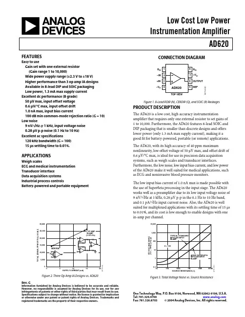
Low Cost Low Power Instrumentation AmplifierAD620Rev. GInformation furnished by Analog Devices is believed to be accurate and reliable. However, no responsibility is assumed by Analog Devices for its use, nor for any infringements of patents or other rights of third parties that may result from its use. Specifications subject to change without notice. No license is granted by implication One Technology Way, P.O. Box 9106, Norwood, MA 02062-9106, U.S.A. Tel: 781.329.4700 FEATURESEasy to useGain set with one external resistor (Gain range 1 to 10,000)Wide power supply range (±2.3 V to ±18 V) Higher performance than 3 op amp IA designs Available in 8-lead DIP and SOIC packaging Low power, 1.3 mA max supply current Excellent dc performance (B grade) 50 µV max, input offset voltage 0.6 µV/°C max, input offset drift 1.0 nA max, input bias current100 dB min common-mode rejection ratio (G = 10) Low noise9 nV/√Hz @ 1 kHz, input voltage noise 0.28 µV p-p noise (0.1 Hz to 10 Hz) Excellent ac specifications120 kHz bandwidth (G = 100) 15 µs settling time to 0.01%APPLICATIONSWeigh scalesECG and medical instrumentation Transducer interface Data acquisition systems Industrial process controlsBattery-powered and portable equipmentCONNECTION DIAGRAM–IN R G –V S+IN R G+V S OUTPUTREFTOP VIEW00775-0-001Figure 1. 8-Lead PDIP (N), CERDIP (Q), and SOIC (R) PackagesPRODUCT DESCRIPTIONThe AD620 is a low cost, high accuracy instrumentationamplifier that requires only one external resistor to set gains of 1 to 10,000. Furthermore, the AD620 features 8-lead SOIC and DIP packaging that is smaller than discrete designs and offers lower power (only 1.3 mA max supply current), making it a good fit for battery-powered, portable (or remote) applications. The AD620, with its high accuracy of 40 ppm maximumnonlinearity, low offset voltage of 50 µV max, and offset drift of 0.6 µV/°C max, is ideal for use in precision data acquisition systems, such as weigh scales and transducer interfaces.Furthermore, the low noise, low input bias current, and low power of the AD620 make it well suited for medical applications, such as ECG and noninvasive blood pressure monitors.The low input bias current of 1.0 nA max is made possible with the use of Superϐeta processing in the input stage. The AD620 works well as a preamplifier due to its low input voltage noise of 9 nV/√Hz at 1 kHz, 0.28 µV p-p in the 0.1 Hz to 10 Hz band, and 0.1 pA/√Hz input current noise. Also, the AD620 is well suited for multiplexed applications with its settling time of 15 µs to 0.01%, and its cost is low enough to enable designs with one in-amp per channel.30,0005,00010,00015,00020,00025,000T O T A L E R R O R , P P M O F F U L L S C A L ESUPPLY CURRENT (mA)00000Figure 2. Three Op Amp IA Designs vs. AD620SOURCE RESISTANCE (Ω)R T I V O L T A G E N O I S E (0.1– 10H z ) (µV p -p )00000Figure 3. Total Voltage Noise vs. Source ResistanceAD620TABLE OF CONTENTSSpecifications (3)Absolute Maximum Ratings (5)ESD Caution (5)Typical Performance Characteristics (7)Theory of Operation (13)Gain Selection (16)Input and Output Offset Voltage (16)Reference Terminal (16)Input Protection (16)RF Interference (16)Common-Mode Rejection (17)Grounding (17)Ground Returns for Input Bias Currents (18)Outline Dimensions (19)Ordering Guide (20)REVISION HISTORY12/04—Rev. F to Rev. GUpdated Format..................................................................Universal Change to Features. (1)Change to Product Description (1)Changes to Specifications (3)Added Metallization Photograph (4)Replaced Figure 4-Figure 6 (6)Replaced Figure 15 (7)Replaced Figure 33 (10)Replaced Figure 34 and Figure 35 (10)Replaced Figure 37 (10)Changes to Table 3 (13)Changes to Figure 41 and Figure 42 (14)Changes to Figure 43 (15)Change to Figure 44 (17)Changes to Input Protection section (15)Deleted Figure 9 (15)Changes to RF Interference section (15)Edit to Ground Returns for Input Bias Currents section (17)Added AD620CHIPS to Ordering Guide....................................19 7/03—Data Sheet changed from REV. E to REV. FEdit to FEATURES (1)Changes to SPECIFICATIONS (2)Removed AD620CHIPS from ORDERING GUIDE (4)Removed METALLIZATION PHOTOGRAPH (4)Replaced TPCs 1–3 (5)Replaced TPC 12 (6)Replaced TPC 30 (9)Replaced TPCs 31 and 32 (10)Replaced Figure 4 (10)Changes to Table I (11)Changes to Figures 6 and 7 (12)Changes to Figure 8 (13)Edited INPUT PROTECTION section (13)Added new Figure 9 (13)Changes to RF INTERFACE section (14)Edit to GROUND RETURNS FOR INPUT BIAS CURRENTS section (15)Updated OUTLINE DIMENSIONS (16)AD620 SPECIFICATIONSTypical @ 25°C, V S = ±15 V, and R L = 2 kΩ, unless otherwise noted.Table 1.AD620A AD620B AD620S1Parameter ConditionsMin Typ Max Min Typ Max Min Typ Max Unit GAIN G = 1 + (49.4 kΩ/R G)Gain Range 1 10,000 1 10,000 1 10,000Gain Error2V OUT = ±10 VG = 1 0.03 0.10 0.01 0.02 0.03 0.10 %G = 10 0.15 0.30 0.10 0.15 0.15 0.30 %G = 100 0.15 0.30 0.10 0.15 0.15 0.30 %G = 1000 0.40 0.70 0.35 0.50 0.40 0.70 % Nonlinearity V OUT = −10 V to +10 VG = 1–1000 R L = 10 kΩ 10 40 10 40 10 40 ppmG = 1–100 R L = 2 kΩ 10 95 10 95 10 95 ppm Gain vs. TemperatureG = 1 10 10 10 ppm/°C>12−50 −50 −50 ppm/°C GainVOLTAGE OFFSET (Total RTI Error = V OSI + V OSO/G)30 125 15 50 30 125 µV Input Offset, V OSI V S = ±5 Vto ± 15 VOvertemperature V S = ±5 V185 85 225 µV to ± 15 V0.3 1.0 0.1 0.6 0.3 1.0 µV/°CAverage TC V S = ±5 Vto ± 15 VOutput Offset, V OSO V S = ±15 V 400 1000 200 500 400 1000 µV V S = ± 5 V 1500 750 1500 µV Overtemperature V S = ±5 V2000 1000 2000 µV to ± 15 V5.0 15 2.5 7.0 5.0 15 µV/°CAverage TC V S = ±5 Vto ± 15 VOffset Referred to theInput vs. Supply (PSR) V S = ±2.3 Vto ±18 VG = 1 80 100 80 100 80 100 dBG = 10 95 120 100 120 95 120 dBG = 100 110 140 120 140 110 140 dBG = 1000 110 140 120 140 110 140 dB INPUT CURRENTInput Bias Current 0.5 2.0 0.5 1.0 0.5 2 nA Overtemperature 2.5 1.5 4 nA Average TC 3.0 3.0 8.0 pA/°C Input Offset Current 0.3 1.0 0.3 0.5 0.3 1.0 nA Overtemperature 1.5 0.75 2.0 nA Average TC 1.5 1.5 8.0 pA/°C INPUTInput ImpedanceDifferential 10||2 10||2 10||2 GΩ_pF Common-Mode 10||2 10||2 10||2 GΩ_pF−V S + 1.9 +V S − 1.2 −V S + 1.9 +V S − 1.2 −V S + 1.9 +V S − 1.2 V Input Voltage Range3V S = ±2.3 Vto ±5 VOvertemperature −V S + 2.1 +V S − 1.3 −V S + 2.1 +V S − 1.3 −V S + 2.1 +V S − 1.3 V V S = ± 5 V−V S + 1.9 +V S − 1.4 −V S + 1.9 +V S − 1.4 −V S + 1.9 +V S − 1.4 V to ±18 VOvertemperature −V S + 2.1 +V S − 1.4 −V S + 2.1 +V S + 2.1 −V S + 2.3 +V S − 1.4 VAD620AD620A AD620B AD620S1Parameter ConditionsMin Typ Max Min Typ Max Min Typ Max Unit1 See Analog Devices military data sheet for 883B tested specifications.2 Does not include effects of external resistor R G.3 One input grounded. G = 1.4 This is defined as the same supply range that is used to specify PSR.AD620ABSOLUTE MAXIMUM RATINGSTable 2.Parameter RatingSupply Voltage ±18 VInternal Power Dissipation 1 650 mWInput Voltage (Common-Mode) ±V SDifferential Input Voltage 25 VOutput Short-Circuit Duration IndefiniteStorage Temperature Range (Q) −65°C to +150°CStorage Temperature Range (N, R) −65°C to +125°COperating Temperature Range AD620 (A, B) −40°C to +85°C AD620 (S) −55°C to +125°C Lead Temperature Range (Soldering 10 seconds) 300°C1Specification is for device in free air: 8-Lead Plastic Package: θJA = 95°C 8-Lead CERDIP Package: θJA = 110°C 8-Lead SOIC Package: θJA = 155°CStresses above those listed under Absolute Maximum Ratings may cause permanent damage to the device. This is a stress rating only; functional operation of the device at these or any other condition s above those indicated in the operational section of this specification is not implied. Exposure to absolute maximum rating conditions for extended periods may affect device reliability.ESD CAUTIONESD (electrostatic discharge) sensitive device. Electrostatic charges as high as 4000 V readily accumulate on the human body and test equipment and can discharge without detection. Although this product features proprietary ESD protection circuitry, permanent damage may occur on devices subjected to high energy electrostatic discharges. Therefore, proper ESD precautions are recommended to avoid performancedegradation or loss of functionality.AD62000775-0-004Figure 4. Metallization Photograph. Dimensions shown in inches and (mm). Contact sales for latest dimensions.AD620TYPICAL PERFORMANCE CHARACTERISTICS(@ 25°C, V S = ±15 V , R L = 2 kΩ, unless otherwise noted.)INPUT OFFSET VOLTAGE (µV)20304050P E R C E N T A G E O F U N I T S1000775-0-005Figure 5. Typical Distribution of Input Offset VoltageINPUT BIAS CURRENT (pA)1020304050–600600P E R C E N T A G E O F U N I T S–1200120000775-0-006Figure 6. Typical Distribution of Input Bias Current1020304050INPUT OFFSET CURRENT (pA)P E R C E N T A G E O F U N I T S00775-0-Figure 7. Typical Distribution of Input Offset Current TEMPERATURE (°C)I N P U T B I A S C U R R E N T (n A )+I B–I B2.0–2.0175–1.0–1.5–75–0.500.51.01.51257525–2500775-0-008Figure 8. Input Bias Current vs. TemperatureC H A N G E I N O F F S E T V O L T A G E (µV )1.50.5WARM-UP TIME (Minutes)2.0011.0432500775-0-009Figure 9. Change in Input Offset Voltage vs. Warm-Up TimeFREQUENCY (Hz)V O L T A G E N O I S E (n V / H z )00775-0-010Figure 10. Voltage Noise Spectral Density vs. Frequency (G = 1−1000)AD620FREQUENCY (Hz)1000100101101000100C U R R E N T N O I S E (f A / H z )00775-0-011Figure 11. Current Noise Spectral Density vs. FrequencyR T IN O I S E (2.0µV /D I V )TIME (1 SEC/DIV)00775-0-012Figure 12. 0.1 Hz to 10 Hz RTI Voltage Noise (G = 1) R T I N O I S E (0.1µV /D I V )TIME (1 SEC/DIV)00775-0-013Figure 13. 0.1 Hz to 10 Hz RTI Voltage Noise (G = 1000) 00775-0-014Figure 14. 0.1 Hz to 10 Hz Current Noise, 5 pA/Div1001000AD620AFET INPUT IN-AMPSOURCE RESISTANCE (Ω)T O T A L D R I F T F R O M 25°C T O 85°C , R T I (µV )100,000101k10M10,00010k1M100k 00775-0-015Figure 15. Total Drift vs. Source ResistanceFREQUENCY (Hz)C M R (d B )16001M80401600.1140100120100k 10k 1k 100102000775-0-016Figure 16. Typical CMR vs. Frequency, RTI, Zero to 1 kΩ Source ImbalanceAD620FREQUENCY (Hz)P S R (d B )1601M80401600.1140100120100k 10k 1k 100102018000775-0-017Figure 17. Positive PSR vs. Frequency, RTI (G = 1−1000)FREQUENCY (Hz)P S R (d B )1601M80401600.1140100120100k10k1k 100102018000775-0-018Figure 18. Negative PSR vs. Frequency, RTI (G = 1−1000)100010010M10011k10100k 1M 10k FREQUENCY (Hz)GA I N (V /V )0.100775-0-019Figure 19. Gain vs. Frequency O U T P U T V O L T A G E (V p -p )FREQUENCY (Hz)351551030202500775-0-020Figure 20. Large Signal Frequency ResponseI N P U T V O L T A G E L I M I T (V )(R E F E R R E D T OS U P P L Y V O L T A G E S )SUPPLY VOLTAGE ± Volts+V S –V S 00775-Figure 21. Input Voltage Range vs. Supply Voltage, G = 120501510SUPPLY VOLTAGE ± VoltsO U T P U T V O L T A G E S W I N G (V )(R E F E R R E D T O S U P P L Y V O L T A G E S )+V S –V S 00775-0Figure 22. Output Voltage Swing vs. Supply Voltage, G = 10AD620O U T P U T V O L T A G E S W I N G (V p -p )LOAD RESISTANCE (Ω)300010k20101001k00775-0-023Figure 23. Output Voltage Swing vs. Load Resistance00775-0-024Figure 24. Large Signal Pulse Response and Settling TimeG = 1 (0.5 mV = 0.01%)00775-0-025Figure 25. Small Signal Response, G = 1, R L = 2 kΩ, C L= 100 pF00775-0-026Figure 26. Large Signal Response and Settling Time, G = 10 (0.5 mV = 0.01%)00775-0-027Figure 27. Small Signal Response, G = 10, R L = 2 kΩ, C L = 100 pF00775-0-030Figure 28. Large Signal Response and Settling Time, G = 100 (0.5 mV = 0.01%)00775-0-029Figure 29. Small Signal Pulse Response, G = 100, R L = 2 kΩ, C L = 100 pF00775-0-030Figure 30. Large Signal Response and Settling Time,G = 1000 (0.5 mV = 0.01% )00775-0-031Figure 31. Small Signal Pulse Response, G = 1000, R L = 2 kΩ, C L = 100 pF OUTPUT STEP SIZE (V)S E T T L I N G T I M E (µs )TO 0.01%TO 0.1%2002155510101500775-0-032Figure 32. Settling Time vs. Step Size (G = 1)GAINS E T T L I N G T I M E (µs )1000111000100101010000775-0-033Figure 33. Settling Time to 0.01% vs. Gain, for a 10 V Step00775-0-034Figure 34. Gain Nonlinearity, G = 1, R L = 10 kΩ (10 µV = 1 ppm)00775-0-035Figure 35. Gain Nonlinearity, G = 100, R L = 10 kΩ(100 µV = 10 ppm)00775-0-036Figure 36. Gain Nonlinearity, G = 1000, R L = 10 kΩ(1 mV = 100 ppm)1k Ω10k Ω*ALL RESISTORS 1% TOLERANCE00Figure 37. Settling Time Test CircuitTHEORY OF OPERATIONS REF775--38Figure 38. Simplified Schematic of AD620The AD620 is a monolithic instrumentation amplifier based on a modification of the classic three op amp approach. Absolute value trimming allows the user to program gain accurately(to 0.15% at G = 100) with only one resistor. Monolithic construction and laser wafer trimming allow the tight matching and tracking of circuit components, thus ensuring the high level of performance inherent in this circuit. The input transistors Q1 and Q2 provide a single differential-pair bipolar input for high precision (Figure 38), yet offer 10× lower input bias current thanks to Superϐeta processing. Feedback through the Q1-A1-R1 loop and the Q2-A2-R2 loop maintains constant collector current of the input devices Q1 and Q2, thereby impressing the input voltage across the external gain setting resistor R G. This creates a differential gain from the inputs to the A1/A2 outputs given by G = (R1 + R2)/R G + 1. The unity-gain subtractor, A3, removes any common-mode signal, yielding a single-ended output referred to the REF pin potential. The value of R G also determines the transconductance of the preamp stage. As R G is reduced for larger gains, the transconductance increases asymptotically to that of the input transistors. This has three important advantages: (a) Open-loop gain is boosted for increasing programmed gain, thus reducing gain related errors. (b) The gain-bandwidth product (determined by C1 and C2 and the preamp transconductance) increases with programmed gain, thus optimizing frequency response. (c) The input voltage noise is reduced to a value of9 nV/√Hz, determined mainly by the collector current and base resistance of the input devices.The internal gain resistors, R1 and R2, are trimmed to an absolute value of 24.7 kΩ, allowing the gain to be programmed accurately with a single external resistor.The gain equation is then14.49+Ω=GRkG14.49−Ω=GkRGMake vs. Buy: a Typical Bridge Application Error Budget The AD620 offers improved performance over “homebrew” three op amp IA designs, along with smaller size, fewer components, and 10× lower supply current. In the typical application, shown in Figure 39, a gain of 100 is required to amplify a bridge output of 20 mV full-scale over the industrial temperature range of −40°C to +85°C. Table 3 shows how to calculate the effect various error sources have on circuit accuracy.Regardless of the system in which it is being used, the AD620 provides greater accuracy at low power and price. In simple systems, absolute accuracy and drift errors are by far the most significant contributors to error. In more complex systems with an intelligent processor, an autogain/autozero cycle will remove all absolute accuracy and drift errors, leaving only the resolution errors of gain, nonlinearity, and noise, thus allowing full 14-bit accuracy.Note that for the homebrew circuit, the OP07 specifications for input voltage offset and noise have been multiplied by √2. This is because a three op amp type in-amp has two op amps at its inputs, both contributing to the overall input error.PRECISION BRIDGE TRANSDUCER00775-0-039AD620A MONOLITHIC INSTRUMENTATION AMPLIFIER, G = 100SUPPLY CURRENT = 1.3mA MAX00775-0-040Figure 39. Make vs. Buy"HOMEBREW" IN-AMP, G = 100*0.02% RESISTOR MATCH, 3ppm/°C TRACKING **DISCRETE 1% RESISTOR, 100ppm/°C TRACKING SUPPLY CURRENT = 15mA MAX0000Table 3. Make vs. Buy Error BudgetError, ppm of Full Scale Error SourceAD620 Circuit Calculation “Homebrew” Circuit Calculation AD620 Homebrew ABSOLUTE ACCURACY at T A = 25°CInput Offset Voltage, µV 125 µV/20 mV(150 µV × √2)/20 mV 6,250 10,607 Output Offset Voltage, µV 1000 µV/100 mV/20 mV ((150 µV × 2)/100)/20 mV 500 150 Input Offset Current, nA 2 nA ×350 Ω/20 mV(6 nA ×350 Ω)/20 mV18 53 CMR, dB 110 dB(3.16 ppm) ×5 V/20 mV (0.02% Match × 5 V)/20 mV/100 791 500Total Absolute Error 7,559 11,310DRIFT TO 85°CGain Drift, ppm/°C(50 ppm + 10 ppm) ×60°C 100 ppm/°C Track × 60°C 3,600 6,000 Input Offset Voltage Drift, µV/°C 1 µV/°C × 60°C/20 mV(2.5 µV/°C × √2 × 60°C)/20 mV3,000 10,607 Output Offset Voltage Drift, µV/°C 15 µV/°C × 60°C/100 mV/20 mV (2.5 µV/°C × 2 × 60°C)/100 mV/20 mV 450 150Total Drift Error 7,050 16,757RESOLUTIONGain Nonlinearity, ppm of Full Scale40 ppm40 ppm40 40 Typ 0.1 Hz to 10 Hz Voltage Noise, µV p-p 0.28 µV p-p/20 mV (0.38 µV p-p × √2)/20 mV 14 27 Total Resolution Error 54 67Grand Total Error 14,663 28,134G = 100, V S = ±15 V .(All errors are min/max and referred to input.)Figure 40. A Pressure Monitor Circuit that Operates on a 5 V Single SupplyPressure MeasurementAlthough useful in many bridge applications, such as weigh scales, the AD620 is especially suitable for higher resistance pressure sensors powered at lower voltages where small size and low power become more significant.Figure 40 shows a 3 kΩ pressure transducer bridge powered from 5 V . In such a circuit, the bridge consumes only 1.7 mA. Adding the AD620 and a buffered voltage divider allows the signal to be conditioned for only 3.8 mA of total supply current. Small size and low cost make the AD620 especially attractive for voltage output pressure transducers. Since it delivers low noise and drift, it will also serve applications such as diagnostic noninvasive blood pressure measurement.Medical ECGThe low current noise of the AD620 allows its use in ECGmonitors (Figure 41) where high source resistances of 1 MΩ or higher are not uncommon. The AD620’s low power, low supply voltage requirements, and space-saving 8-lead mini-DIP and SOIC package offerings make it an excellent choice for battery-powered data recorders.Furthermore, the low bias currents and low current noise, coupled with the low voltage noise of the AD620, improve the dynamic range for better performance.The value of capacitor C1 is chosen to maintain stability of the right leg drive loop. Proper safeguards, such as isolation, must be added to this circuit to protect the patient from possible harm.Figure 41. A Medical ECG Monitor CircuitPrecision V-I ConverterThe AD620, along with another op amp and two resistors, makes a precision current source (Figure 42). The op amp buffers the reference terminal to maintain good CMR. The output voltage, V X , of the AD620 appears across R1, which converts it to a current. This current, less only the input bias current of the op amp, then flows out to the load.V IN+V 00775-0-044Figure 42. Precision Voltage-to-Current Converter (Operates on 1.8 mA, ±3 V)GAIN SELECTIONThe AD620’s gain is resistor-programmed by R G , or moreprecisely, by whatever impedance appears between Pins 1 and 8. The AD620 is designed to offer accurate gains using 0.1% to 1% resistors. Table 4 shows required values of R G for various gains. Note that for G = 1, the R G pins are unconnected (R G = ∞). For any arbitrary gain, R G can be calculated by using the formula:14.49−Ω=G k R GTo minimize gain error, avoid high parasitic resistance in series with R G ; to minimize gain drift, R G should have a low TC—less than 10 ppm/°C—for the best performance.Table 4. Required Values of Gain Resistors1% Std Table Value of R G (Ω) Calculated Gain 0.1% Std Table Value of R G (Ω ) Calculated Gain 49.9 k 1.990 49.3 k 2.002 12.4 k 4.984 12.4 k 4.984 5.49 k 9.998 5.49 k 9.998 2.61 k 19.93 2.61 k 19.93 1.00 k 50.40 1.01 k 49.91 499 100.0 499 100.0 249 199.4 249 199.4 100 495.0 98.8 501.0 49.9991.049.31,003.0INPUT AND OUTPUT OFFSET VOLTAGEThe low errors of the AD620 are attributed to two sources,input and output errors. The output error is divided by G when referred to the input. In practice, the input errors dominate at high gains, and the output errors dominate at low gains. The total V OS for a given gain is calculated asTotal Error RTI = input error + (output error/G) Total Error RTO = (input error × G) + output errorREFERENCE TERMINALThe reference terminal potential defines the zero output voltage and is especially useful when the load does not share a precise ground with the rest of the system. It provides a direct means of injecting a precise offset to the output, with an allowable range of 2 V within the supply voltages. Parasitic resistance should be kept to a minimum for optimum CMR.INPUT PROTECTIONThe AD620 features 400 Ω of series thin film resistance at itsinputs and will safely withstand input overloads of up to ±15 V or ±60 mA for several hours. This is true for all gains and power on and off, which is particularly important since the signal source and amplifier may be powered separately. For longer time periods, the current should not exceed 6 mA(I IN ≤ V IN /400 Ω). For input overloads beyond the supplies, clamping the inputs to the supplies (using a low leakage diode such as an FD333) will reduce the required resistance, yielding lower noise.RF INTERFERENCEAll instrumentation amplifiers rectify small out of band signals. The disturbance may appear as a small dc voltage offset. High frequency signals can be filtered with a low pass R-C network placed at the input of the instrumentation amplifier. Figure 43 demonstrates such a configuration. The filter limits the input signal according to the following relationship:)2(21C D DIFF C C R FilterFreq +π=CCM RC FilterFreq π=21where C D ≥10C C.C D affects the difference signal. C C affects the common-mode signal. Any mismatch in R × C C will degrade the AD620’s CMRR. To avoid inadvertently reducing CMRR-bandwidth performance, make sure that C C is at least one magnitudesmaller than C D . The effect of mismatched C C s is reduced with a larger C D :C C ratio.Figure 43. Circuit to Attenuate RF Interference COMMON-MODE REJECTIONInstrumentation amplifiers, such as the AD620, offer high CMR, which is a measure of the change in output voltage when both inputs are changed by equal amounts. These specifications are usually given for a full-range input voltage change and a specified source imbalance.For optimal CMR, the reference terminal should be tied to a low impedance point, and differences in capacitance and resistance should be kept to a minimum between the two inputs. In many applications, shielded cables are used to minimize noise; for best CMR over frequency, the shield should be properly driven. Figure 44 and Figure 45 show active data guards that are configured to improve ac common-mode rejections by “bootstrapping” the capacitances of input cable shields, thus minimizing the capacitance mismatch between the inputs.V OUT775--46Figure 44. Differential Shield DriverOUT775--47Figure 45. Common-Mode Shield Driver GROUNDINGSince the AD620 output voltage is developed with respect to the potential on the reference terminal, it can solve many grounding problems by simply tying the REF pin to the appropriate “local ground.”To isolate low level analog signals from a noisy digital environment, many data-acquisition components have separate analog and digital ground pins (Figure 46). It would be convenient to use a single ground line; however, current through ground wires and PC runs of the circuit card can cause hundreds of millivolts of error. Therefore, separate ground returns should be provided to minimize the current flow from the sensitive points to the system ground. These ground returns must be tied together at some point, usually best at the ADC package shown in Figure 46.DIGITALDATAOUTPUT775--48Figure 46. Basic Grounding PracticeGROUND RETURNS FOR INPUT BIAS CURRENTSInput bias currents are those currents necessary to bias the input transistors of an amplifier. There must be a direct return path for these currents. Therefore, when amplifying “floating” input sources, such as transformers or ac-coupled sources, there must be a dc path from each input to ground, as shown in Figure 47, Figure 48, and Figure 49. Refer to A Designer’s Guide to Instrumentation Amplifiers (free from Analog Devices) for more information regarding in-amp applications.Figure 47. Ground Returns for Bias Currents with Transformer-Coupled InputsTO POWER SUPPLY GROUND+V 00775-0-050Figure 48. Ground Returns for Bias Currents with Thermocouple InputsFigure 49. Ground Returns for Bias Currents with AC-Coupled InputsOUTLINE DIMENSIONSCOMPLIANT TO JEDEC STANDARDS MS-001-BA0.070 (1.78)0.060 (1.52)0.045 (1.14)MAXCONTROLLING DIMENSIONS ARE IN INCHES; MILLIMETER DIMENSIONS (IN PARENTHESES) ARE ROUNDED-OFF INCH EQUIVALENTS FORREFERENCE ONLY AND ARE NOT APPROPRIATE FOR USE IN DESIGN.CORNER LEADS MAY BE CONFIGURED AS WHOLE OR HALF LEADS.Figure 50. 8-Lead Plastic Dual In-Line Package [PDIP] Narrow Body (N-8).Dimensions shown in inches and (millimeters)CONTROLLING DIMENSIONS ARE IN INCHES; MILLIMETER DIMENSIONS (IN PARENTHESES) ARE ROUNDED-OFF INCH EQUIVALENTS FORREFERENCE ONLY AND ARE NOT APPROPRIATE FOR USE IN DESIGN0.005 (0.13)0.055 (1.40)Figure 51. 8-Lead Ceramic Dual In-Line Package [CERDIP] (Q-8)Dimensions shown in inches and (millimeters)CONTROLLING DIMENSIONS ARE IN MILLIMETERS; INCH DIMENSIONS (IN PARENTHESES) ARE ROUNDED-OFF MILLIMETER EQUIVALENTS FOR REFERENCE ONLY AND ARE NOT APPROPRIATE FOR USE IN DESIGNCOMPLIANT TO JEDEC STANDARDS MS-012AAFigure 52. 8-Lead Standard Small Outline Package [SOIC]Narrow Body (R-8)Dimensions shown in millimeters and (inches)。