
91A1AF22D18R51中文资料
- 格式:pdf
- 大小:339.88 KB
- 文档页数:3

PLA191
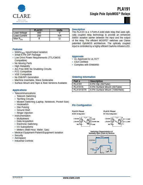
DS-PLA191-R1The PLA191 is a 1-Form-Asolid state relay that uses opti-cally coupled relay technology to provide an enhanced5000V isolation barrier between the input and the output of the relay. The efficient MOSFETswitches use Clarespatented OptoMOS architecture. The optically coupledinput is controlled by a highly efficient GaAIAs infrared LED.
•Telecommunications•Telecom Switching•Tip/Ring Circuits•Modem Switching (Laptop, Notebook, Pocket Size)•Hookswitch•Dial Pulsing•Ground Start•Ringer Injection•Instrumentation•Multiplexers•Data Acquisition•Electronic Switching•I/O Subsystems•Meters (Watt-Hour, Water, Gas)•Medical Equipment-Patient/Equipment Isolation•Security•Aerospace•Industrial Controls•ULApproved to UL1577•CSACertified•Complies with EN60950•5000VRMSInput/Output Isolation•Small 6 Pin DIPPackage•Low Drive Power Requirements (TTL/CMOS Compatible)•No Moving Parts•High Reliability•Arc-Free With No Snubbing Circuits•FCC Compatible•VDE Compatible•No EMI/RFI Generation•Machine Insertable, Wave Solderable•Surface Mount and Tape & Reel Versions Available

IntegratedCircuitSystems, Inc.
General DescriptionFeatures AV9170
Block DiagramClock Synchronizer and Multiplier
AV 9170 Rev E 9/24/99On-chip Phase-Locked Loop for clocks synchronizationSynchronizes frequencies up to 107 MHz(output) @ 5.0V±1ns skew (max) between input & output clocks @ 5.0VCan recover poor duty cycle clocksCLK1 to CLK2 skew controlled to within ±1ns @ 5.0V3.0 - 5.5V supply rangeLow power CMOS technologySmall 8-pin DIP or SOIC packageOn chip loop filterAV9170-01, -04 for output clocks 20-107 MHz @ 5.0V,20 - 66.7 MHz @ 3.3VAV9170-02, -05 for output clocks 5-26.75 MHz @ 5.0V,5 - 16.7 MHz @ 3.3VThe AV9170 generates an output clock which is synchronizedto a given continuous input clock with zero delay (±1ns at 5VVDD). Using ICSs proprietary phase-locked loop (PLL) ana-log CMOS technology, the AV9170 is useful for regeneratingclocks in high speed systems where skew is a major concern.By the use of the two select pins, multiples or divisions of theinput clock can be generated with zero delay (see Tables 2 and3). The standard versions produce two outputs, where CLK2is always a divide by two version of CLK1.The AV9170 is also useful to recover poor duty cycle clocks.A 50 MHz signal with a 20/80% duty cycle, for example, canbe regenerated to the 48/52% typical of the part.The AV9170 allows the user to control the PLL feedback,making it possible, with an additional 74F240 octal buffer (orother such device that offers controlled skew outputs), tosynchronize up to 8 output clocks with zero delay compared tothe input (see Figure 1). Application notes for the AV9170 areavailable. Please consult ICS.ICS reserves the right to make changes in the device data identified in this publicationwithout further notice. ICS advises its customers to obtain the latest version of alldevice data to verify that any information being relied upon by the customer is currentand accurate.元器件交易网
Ver: 1.0 Oct 02, 2002 TEL: 886-3-5788833 1
Global Mixed-mode Technology Inc. G781
±1°C Remote and Local Temperature Sensor with SMBus Serial Interface
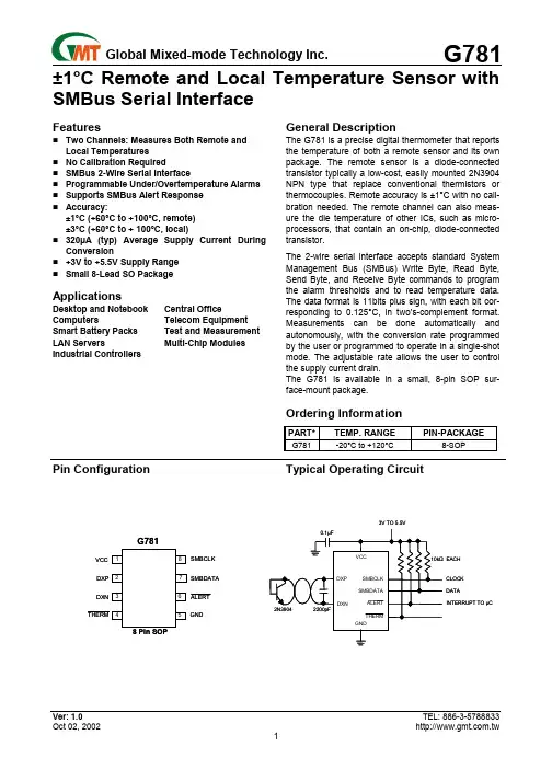
Features Two Channels: Measures Both Remote and Local Temperatures No Calibration Required SMBus 2-Wire Serial Interface Programmable Under/Overtemperature Alarms Supports SMBus Alert Response Accuracy: ±1°C (+60°C to +100°C, remote) ±3°C (+60°C to + 100°C, local) 320µA (typ) Average Supply Current During Conversion +3V to +5.5V Supply Range Small 8-Lead SO Package Applications Desktop and Notebook Central Office Computers Telecom Equipment Smart Battery Packs Test and Measurement LAN Servers Multi-Chip Modules Industrial Controllers General Description The G781 is a precise digital thermometer that reports the temperature of both a remote sensor and its own package. The remote sensor is a diode-connected transistor typically a low-cost, easily mounted 2N3904 NPN type that replace conventional thermistors or thermocouples. Remote accuracy is ±1°C with no cali-bration needed. The remote channel can also meas-ure the die temperature of other ICs, such as micro-processors, that contain an on-chip, diode-connected transistor. The 2-wire serial interface accepts standard System Management Bus (SMBus) Write Byte, Read Byte, Send Byte, and Receive Byte commands to program the alarm thresholds and to read temperature data. The data format is 11bits plus sign, with each bit cor-responding to 0.125°C, in two’s-complement format. Measurements can be done automatically and autonomously, with the conversion rate programmed by the user or programmed to operate in a single-shot mode. The adjustable rate allows the user to control the supply current drain. The G781 is available in a small, 8-pin SOP sur-face-mount package. Ordering Information PART* TEMP. RANGE PIN-PACKAGE G781 -20°C to +120°C 8-SOP Pin Configuration Typical Operating Circuit 10k
Description
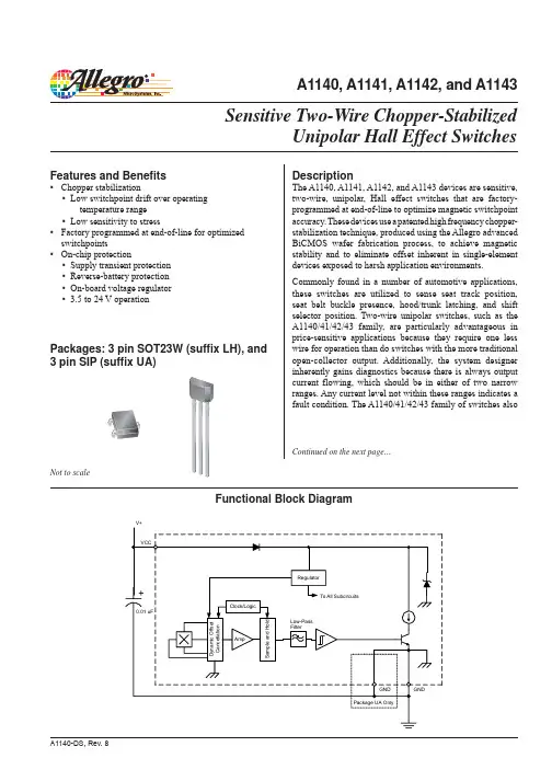
The A1140, A1141, A1142, and A1143 devices are sensitive,
two-wire, unipolar, Hall effect switches that are factory-
programmed at end-of-line to optimize magnetic switchpoint
accuracy. These devices use a patented high frequency chopper-
stabilization technique, produced using the Allegro advanced
BiCMOS wafer fabrication process, to achieve magnetic
stability and to eliminate offset inherent in single-element
devices exposed to harsh application environments.
Commonly found in a number of automotive applications,
these switches are utilized to sense seat track position,
seat belt buckle presence, hood/trunk latching, and shift
selector position. Two-wire unipolar switches, such as the
A1140/41/42/43 family, are particularly advantageous in
price-sensitive applications because they require one less