
allegro pcb design GXL XL L异同
- 格式:doc
- 大小:563.50 KB
- 文档页数:3


时间:2012年12月17日10:00:061.关于制作封装的步骤;1).自定义手动制作:1. 打开Allegro PCB Design GXL,创建Package symbol 及元件封装页面。
2.在Setup选项中,设置gird和DseignParameters中关于现实范围的大小。
范围的设置可以参考下图,extents是指范围,建议从-1000,-1000开始,2000,2000结束,这样可以使原点显示在中间,使得设计更加简便。
另外还要进行个点设置,在同一工具拦下,选择gird,进行设置。
如下图所示:其中gird on为格点显示按钮。
用来显示格点。
关于格点的设置可以参看相关笔记-格点设置详解3.在准备工作完成后,执行菜单layout,选择pins放置焊盘,如下图:在padstack里选择焊盘,当然要把自制的焊盘库提前添加到指定的位置才可以。
焊盘库与元件库的添加步骤:在Setup-->User Preference Editer-->Categaies-->path选项中的padpath和psmpath中进行设置。
如下图。
在这些准备完成后,可以进行焊盘的添加,点击padstack,选择焊盘。
如下图:选择要放置的焊盘。
一般以原点作为第一个放置点进行放置,以便容易把握尺寸。
呵呵!如果此时不小心多放置了一个焊盘,就要执行删除操作,或者需要旋转一个角度,可以执行选装操作。
具体的执行步骤如下:删除操作:Edit-->Spin,然后点击空白处,然后选择delete或者使用快捷键ctrl+D,然后选择要删除的焊盘,删除即可。
旋转操作:Edit-->Spin,然后在侧边栏输入旋转角度,或者直接旋转亦可。
另外,关于两个焊盘之间的距离的控制盒测量的操作具体如下;焊盘之间的控制可以通过手动放置移动来控制,也可以在命令栏里通过输入坐标来控制。
输入坐标的指令为:x ——>100 100;输入x后要按enter键后,输入坐标以,100 100.该做标为绝对坐标。
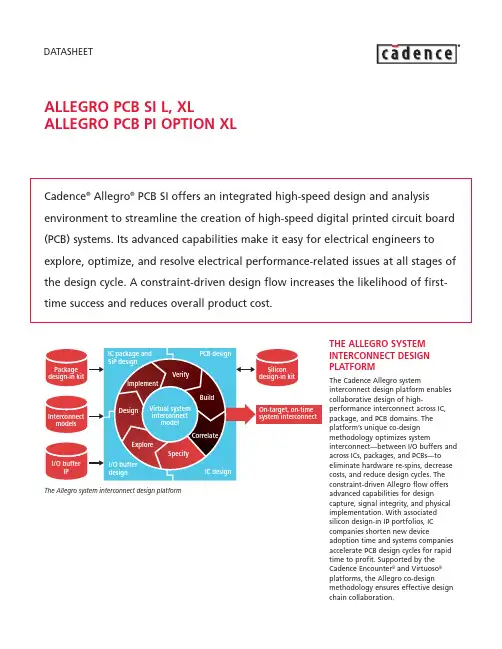
DATASHEETALLEGRO PCB SI L, XLALLEGRO PCB PI OPTION XLCadence®Allegro®PCB SI offers an integrated high-speed design and analysis environment to streamline the creation of high-speed digital printed circuit board (PCB) systems. Its advanced capabilities make it easy for electrical engineers to explore, optimize, and resolve electrical performance-related issues at all stages of the design cycle. A constraint-driven design flow increases the likelihood of first-time success and reduces overall product cost.THE ALLEGRO SYSTEM Array INTERCONNECT DESIGNPLATFORMThe Cadence Allegro systeminterconnect design platform enablescollaborative design of high-performance interconnect across IC,package, and PCB domains. Theplatform’s unique co-designmethodology optimizes systeminterconnect—between I/O buffers andacross ICs, packages, and PCBs—toeliminate hardware re-spins, decreasecosts, and reduce design cycles. Theconstraint-driven Allegro flow offersadvanced capabilities for designcapture, signal integrity, and physicalimplementation. With associatedsilicon design-in IP portfolios, ICcompanies shorten new deviceadoption time and systems companiesaccelerate PCB design cycles for rapidtime to profit. Supported by theCadence Encounter®and Virtuoso®platforms, the Allegro co-designmethodology ensures effective designchain collaboration.ALLEGRO PCB SIAllegro PCB SI provides advanced analysis at the board, multi-board,and/or system level, and across multiple design configurations. It supports the entire high-speed design flow, which includes pre-layout exploration of design parameters such as differential impedance, development of physical parameters, and imprinting of constraints within the PCB database. The result is a true, constraint-driven design flow. Allegro PCB SI integrates tightly with Allegro PCB Editor, Allegro PCB Router, and Allegro Design Entry HDL enabling end-to-end, constraint-driven, high-speed PCB system design.Allegro PCB SI addresses the challenges created as a result of increasing design density, complexity, and faster edge rates by enabling designers to address high-speed issues throughout the design process. This approach allows design teams to eliminate time-consuming simulate-fix-simulate iterations at the back-end of a design. It also enables designers to maximize electrical performance while minimizing cost of the overall product by exploring topologies and models with manufacturing tolerances. Allegro PCB SI allows users to weigh the tradeoffs involved in routing choices (rules) that affect cost relativeto electrical performance andreliability. Once developed, theseoptimal constraints then drive thephysical layout and routing of the PCB.The integrated design and analysisenvironment eliminates the need totranslate design databases to runsimulations. Designers can also addressshrinking timing margins byconsidering the effects of packagedesign on the overall performance ofthe signal from die-to-die. Importantly,the integrated flow allows designersto easily perform post-layoutextraction and verification of complexhigh-speed PCB systems.BENEFITS•Cuts the time required to design high-speed interconnects and increases thelikelihood of first-pass success•Shortens the time required to developoptimum constraints and enables aconstraint-driven PCB design flow•Shortens the time required to design-in advanced devices through the useof Cadence design-in IP portfolios•Improves product performancethrough solution space exploration•Reduces unit costs of end products byusing the Allegro PCB PI Option XL todesign the PCB power delivery systemnetworkFEATURESINTEGRATED HIGH-SPEED DESIGN ANDANALYSISAllegro PCB SI reads and writes to theAllegro PCB Editor database to avoidpossible translation issues and allowsfor constraints and models to beembedded in the board design file.The integrated design and analysissystem is aware of multi-net electricalconstructs from front to back. Forexample, differential pairs andextended nets (nets with a seriestermination) are recognized,extracted, and simulated as oneelectrical net.SOLUTION SPACE EXPLORATIONAllegro PCB SI provides the bestenvironment for users who need todevelop optimal constraints.SigXplorer, a graphical editor thatallows designers to develop constraintsthrough solution space exploration, isthe industry leader in pre-routeanalysis. Solve issues early in thedesign process by using sweptparameter analysis, user-definedstimulus, and custom measurements.SPICE-BASED SIMULATORThe Allegro PCB SI simulationsubsystem includes a SPICE-basedsimulator as well as a powerful macro-modeling capability that combines theadvantages of traditional SPICE-basedstructural modeling with the speed ofbehavioral modeling. An embeddedfield solver models skin effects,proximity/crowding effects, returnpath resistance, and frequency-dependent dielectric constant. Arobust modeling language providesextensibility beyond IBIS for I/O buffersand lossy coupled, frequency-dependent transmission line modelsthat accurately predict the distributedbehavior of PCB traces.BUS ANALYSIS FOR SOURCESYNCHRONOUS SIGNALSAllegro PCB SI provides a quick andeasy way to analyze all the signalsassociated with a source synchronousbus. It shortens the time to simulatevarious configurations (read/write,active, idle) associated with thefunctioning of source synchronousbuses with or without on-dietermination (ODT). It allows signalsto be associated and to save suchassociations with the design database.Allegro PCB SI allows engineers to explore and develop optimum constraints with a constraint-driven design flow23DIE-TO-DIE INTERCONNECT ANALYSIS USING PACKAGE DATABASES Allegro PCB SI supports multi-board configurations for both analysis and constraints, and provides a simple setup process—from motherboard or daughter card connection to a die-to-die configuration. It also supports topology exploration, floorplanning,and post-route verification. CONSTRAINT-DRIVEN PROCESS Allegro Constraint Manager functions within Allegro PCB SI, Allegro Design Entry HDL, and with Allegro PCB Design XL, allowing designers to use constraints developed through solution space exploration to create a constraint-driven physical layout process.MODEL INTEGRITYThe Model Integrity module allows designers to create, manipulate, and validate models quickly in an easy-to-use editing environment. Device model formats supported include:•IBIS 4.1 External Model support for Verilog ®-A, Cadence Spectre ®, HSPICE,Cadence eSpice models •Mentor/Quad XTK•Cadence Device Modeling Language (DML)A Spectre-to-DML conversion module assists in creating DML models from Spectre simulation runs. With the output of the Spectre simulation run,buffer options file, users can quickly create DML models. Model integrity identifies V-I and V-T tables for typical,maximum, and minimum corner casesfrom the Spectre run file. A proven,intelligent best-curve-fitting algorithm provides an accurate DML model. An HSPICE–to-IBIS conversion moduleallows users to create IBIS models from HSPICE simulation runs.I/O BUFFER MODELSSupported I/O buffer model formats include:•Cadence Allegro PCB SI DML•Synopsys HSPICE transistor-levelmodels (requires HSPICE simulator and license, which is not included with Allegro PCB SI)•Spectre transistor-level models(available on Sun Solaris, HP UX, and Linux RHEL 3.0 platforms only). This utilizes an integrated and limited capability version of the Spectre simulator, which is included with Allegro PCB SI XL•IBIS 4.1 External Model support for HSPICE, Spectre, Verilog-A and Cadence DML •Mentor/Quad XTKMENTOR BOARD STATION FLOW Allegro PCB SI can be used inconjunction with the Mentor Board Station PCB design system to provide high-speed design and analysis within a Mentor-based PCB designenvironment. Allegro PCB SI is used to perform high-speed analysis and to define the high-speed design rules used to drive the Allegro PCB Router.Once the design has been placed and routed in accordance with the high-speed rules, the results are passed back to the Mentor Board Station environment. This allows Allegro PCB SI and the Allegro PCB Router to beAllegro PCB SI allows engineers to explore and develop optimum constraints with a constraint-driven design flowDe s ign implementationS olution s pa c e explorationMo d el d evelopment an d verifi c ation Con s traint-d riven pla c e an d routePo s t-layout verifi c ationCon s traint-d riven FPS pe c ifi c ation s Logi c an d timing d e s ignOptimal c on s traint sCon s traint- d riven phy s i c al implementationused for high-speed design and analysis, while the existing Board Station-based manufacturing output process is used for committing the design to manufacturing.DESIGN-IN IP PORTFOLIOA high-speed design-in IP portfolio shortens design-in time for complex devices with high-speed digital I/O buffers. Cadence pioneered this concept by introducing an IP portfolio for Intel’s 64-bit architecture and today stands as the industry leader in offering this kind of complete solution. Design-in IP portfolio contains ready-to-simulate topologies with pre-validated models, layout constraints embedded in a sample PCB file to enable constraint-driven layout flows, tutorials, documentation, scripts, and other utilities. A high-speed design-in IP portfolio includes prepackaged, executable specifications for complex IC devices with high-speed I/Os. Cadence collaborates with IC companies to make it easy for systems companies to design-in complex IC devices with high-speed I/Os.PCI EXPRESS DESIGN CHAINAs multi-gigahertz serial interfaces become more common, many systems companies are choosing to use the next-generation PCI bus—PCI Express. The PCI Express design chain provides an environment in which silicon vendors can communicate the design-in requirements for their devices using PCI Express. Systems companies are able to make tradeoffs regarding the performance of member companies’silicon with respect to system requirements.The PCI Express design chain is web-based infrastructure that enables systems companies that design serial links implementing the PCI Express specification to efficiently qualify member companies as candidates for their systems. For more information about other design-in IP portfolios and the PCI Express design chain, visit .INTEL IXP2800 NETWORK PROCESSORDESIGN-IN IP PORTFOLIOIntel and Cadence engineers workedtogether to provide a high-speeddesign-in IP portfolio for Intel’sIXP2800 network processor. Availablefrom Intel and included in thehardware design kit for IXP2800, thedesign-in IP portfolio contains ready-to-simulate system-level topologies forthe buses that interact with thenetwork processor (RDRAM, SPI4.2, PCI,and QDR); correlated silicon models; afully coupled frequency-dependentlossy package; and PCB trace, via, andconnector models to fully simulate andevaluate the signal quality anddegradation issues inherent in designswith high-speed nets. In addition, thedesign-in IP portfolio contains areference board that includes theconstraints for the main buses on theprocessor. This reference board and theconstraint sets can be used to drivefloorplanning, placement, and routingon the target PCB system that uses theIXP2800 networking processor. Theready-to-simulate topologies comewith instructions on how to use thesetopologies, as well as movies that showhow to use the design-in IP portfoliowith Allegro PCB SI. For moreinformation, contact your Intelrepresentative and ask for thehardware design kit (HDK) for theIXP2800 network processor.XILINX VIRTEX II-PRO DESIGN-IN IPPORTFOLIOXilinx and Cadence engineers workedtogether to provide a high-speeddesign-in IP portfolio in Allegro PCB SIformat for multi-gigabit serial RocketI/O transceivers integrated in XilinxVirtex II-Pro FPGAs. The Allegro PCB SIdesign-in IP portfolio helps engineersshorten design cycles and reducesignal integrity problems whenimplementing multi-gigabit serialtransceivers in PCB systems. It containscorrelated silicon models, preconfiguredtopologies ready to simulate, and afully coupled, frequency-dependentlossy package. It also contains PCBtrace, via, and connector models tofully simulate and evaluate the signalquality and degradation issuesinherent in designs with multi-gigabittransceivers. For more information,visit or contact yourXilinx or Cadence representative.POWER DELIVERY SYSTEMDESIGN WITH ALLEGRO PCBPI OPTION XLAllegro PCB PI Option XL module, anadd-on to Allegro PCB SI, is a unique,integrated design and analysisenvironment that takes the guessworkout of quantifying and controllingnoise in power delivery systems. Itallows users to focus on the designinstead of struggling with datatranslation issues between the CADsystem and the analysis engines. Itintegrates proven technology fromSun Microsystems into the Cadencedesign and analysis environment toaddress the power delivery issuesencountered in high-speed design.Allegro PCB PI Option XL embodies amethodology used to design andoptimize frequency-dependentcharacteristics (supply pathimpedance) of power distributionsystems in high-speed PCB design. Itallows users to do quick and easyiterations of “change-simulate-analyze.” The Cadence approach isrooted in the fact that a powerdistribution system’s impedance isfrequency dependent and must beanalyzed and controlled overfrequency ranges of interest. Themaximum supply current and thetolerated voltage ripple are used toderive the main power deliverysystem’s design parameter—the targetimpedance. Optimizing the targetimpedance over the frequency rangein which the system is expected tooperate yields a power delivery systemwithout hot spots.FEATURESSETUP WIZARDThe Setup Wizard gathers all thenecessary pieces for design andanalysis including board outline; layerstack-up; power plane shapes/powerand ground plane pairs; DC netsassociated with the power planes; andcapacitor libraries.4FREQUENCY DOMAIN ANALYSISAllegro PCB PI Option XL combines the right frequency domain analysis engine with the proven, powerful Allegro PCB SI and Allegro PCB Editor design environments. It simulates the problem in the frequency domain to quantify the impedance of the power delivery system across the frequency range of interest. During simulation, it takes into account the entire power delivery system—VRM, bulk capacitors, bypass capacitors, and power planes. It calculates the number and values of decoupling capacitors and guides users in placing them for optimal results. Users can perform single node analysis early in the design cycle to see if the number of capacitors selected can maintain the target impedance over a desired frequency range. And, as capacitors are placed on the board, multi-node simulation, which takes into account the location of the capacitors on the board and the mounted loop inductance, can be easily run.VRM EDITORThe VRM Editor comes with an easy-to-use input inductance calculator and a target impedance calculator. Specify the allowed voltage ripple and dynamic current to compute the target impedance, and the target impedance is shown in the simulation results waveform window. Thesimulation waveform window displaysa target impedance line, which makesit easy to know which regions of thePCB are crossing the target.VOLTAGE RIPPLES IN TIME DOMAINEffectiveness of decoupling capacitorselection and placement can beverified in time domain.COMPLETE DESIGN AND ANALYSISENVIRONMENTAllegro PCB PI Option XL offers aunique approach to the actualdesigning of power distributionsystems. It takes the integratedapproach a step further by making thedebugging of a problem as simple as“click and view.” Clicking on awaveform in the waveform displaywindow highlights the correspondingregion on the PCB and offers asuggestion on the type and number ofcapacitors needed to address theproblem. Results are displayed in thewaveform window. By having a PCBdesign editor integrated with thisanalysis environment, engineers canselect and place decoupling capacitorsin the necessary areas, and thenquickly see the problem resolved.OPERATING SYSTEMSUPPORT•Red Hat Linux 3.0, 4.0•Windows 2000 with Service Pack 4,XP Professional•Sun Solaris 8, 9, 10•HP-UX 11.11i•IBM AIX 5.3CADENCE SERVICES ANDSUPPORT•Cadence application engineers cananswer your technical questions bytelephone, email, or Internet—theycan also provide technical assistanceand custom training•Cadence certified instructors teachover 70 courses and bring their real-world experience into the classroom•Over 25 Internet Learning Series (iLS)online courses allow you the flexibilityof training at your own computer viathe Internet•SourceLink®online customer supportgives you answers to your technicalquestions—24 hours a day, 7 days aweek—including the latest in quarterlysoftware rollups, product changerelease information, technicaldocumentation, solutions, softwareupdates, and moreDESIGN-IN IP PORTFOLIOS ACCELERATE DESIGN START TIME5MAJOR FEATURE SUMMARY FOR ALLEGRO PCB SI PRODUCTSMajor feature summary for Allegro PCB SI XL, Allegro Design Entry HDL SI XL, Allegro PCB SI L, and Allegro PCB PI option XLAllegro Design Entry HDL XL xAssign Models in Schematics xCreate Xnets in Schematics xApply Constraints & Topologies to Schematic for Single-Ended & Differential Nets xSingle-line Topology Editor (Graphical Canvas)x x x xSimulation Setup Advisor x x xModel Integrity: Model Development Environment x x x xModel Integrity: Syntax Checking for IBIS 3.2 and DML x x x xModel Integrity: HSPICE-to-IBIS Conversion x x x xIBIS 4.0 Models Support x x x xQuad Models Translator x x x xMacro-models Support (DML)x x x xSimulation Control: Single-line Simulation x x x xWaveform Viewer x x x xDetailed Simulation Reports (Such as Flight Time, Overshoot, Noise Margin)x x x xCoupled (3 Net) Simulation x x xCoupled (>3nets) Simulation x xSingle Net Pre-layout Extraction from Allegro Design Entry HDL x x x xAllegro Physical Viewer Plus xDifferential Pair Exploration and Simulation x x x xDifferential Pair Pre- and Post-layout Extraction from Allegro PCB Editor x x xDifferential Pair Pre-layout Extraction from Allegro Design Entry HDL x x xDifferential Signal Constraint Capture x x xCoupled Line Simulations x x xCrosstalk Simulation x x xSource Synchronous Bus Analysis (SI Board L & SI XL)x x xSweep Simulations x x xCurrent Probes x x xMultiterminal Black Boxes in Topologies x x xConstraint Development and Capture of Topologies x x xCustom Measurement x x xCustom Stimulus x x xBatch Simulation x xEMControl: Rules Development x xEMControl:Rules Checking x xEMI Differential Simulation x x xAllegro Constraint Manager x x xColor-coded Real-time Feedback on Violations xApply Constraints and Topologies to Board for Single-ended and Differential Nets x xFloorplanner x xConstraint-driven Floorplanning and Routing x xAllegro PCB Router XL xVoltage Ripples in Time Domain xPower Integrity:Design and Analysis Environment xPower Integrity:Decoupling Capacitor Database Setup Wizard xPower Integrity:Impedance Requirements Calculator xPower Integrity:Decoupling Capacitor Selection and Placement Environment xPower Integrity:VRM Editor xPower Integrity:Decoupling Capacitor Library Editor xPower Integrity:Cross-probing Between Waveform Allegro PCB SI Floorplanner xPower Integrity:Frequency Domain Analysis xFOR MORE INFORMATIONContact Cadence sales at 1.800.746.6223or visit foradditional information. To locate aCadence sales office or CadenceChannel Partner in your area, visit/contact_us.© 2006 Cadence Design Systems, Inc. All rights reserved. Cadence, the Cadence logo, Allegro, Encounter, SourceLink, Spectre, Verilog, and Virtuoso are trademarks of Cadence Design Systems, Inc. All others are properties of their respective holders.5549C07/06。
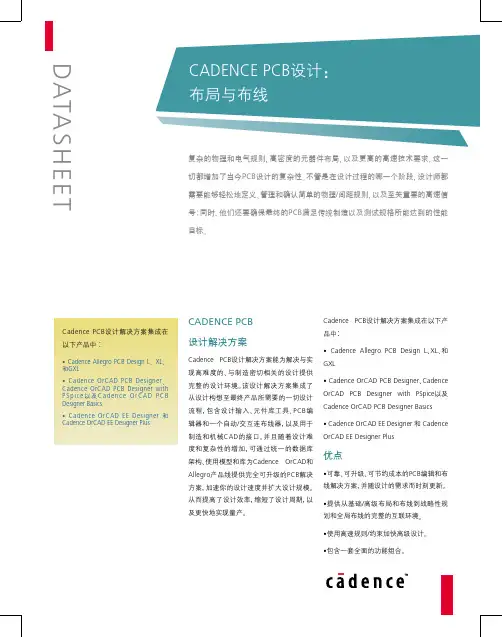
号线的放置和布线过程 该约束管理系统是完全集成到PCB 编辑器中 而约束可以随着设计过程的进行而被实时地确认 确认过程的结果是用图形化的方式表示约束条件是否满足 满足约束用绿色显示 不满足约束就用红色显示 这可使设计师可以及时地看到设计的进度 以及因电子数据表中任何设计变动而产生的影响 布图规划与布局约束和规则驱动的方法有利于强大而灵活的布局功能 包括互动和自动的元件布局 工程师或设计师可以在设计输入或布图规划阶段将元件或支电路分配到特定的 区域 可以通过REF 封装方式 相关信号名 零件号码或原理图表/页面号码来过滤或选择元件 当今的电路板上有成千上万种元器件 需要精确的管理 通过实时的器件装配分析和反馈 得以实现器件装配时从整体上来考虑并满足EMS 规则 以提高设计师的设计速度和效率 DFA(可装配型设计)分析 Allegro PCB Design XL 和GXL 有提供 实现了在互动式元件放置时 实时地进图1 Cadence PCB 设计解决方案集成了从简单到复杂PCB 设计所需的所有工具 行DFA 规则检查 基于一个器件类型和封装排列的二维电子表格 DFA 可以实时地检查器件的边到边 边到端或端到端的距离是否违反最小要求 使得PCB 设计师可以同步地放置元器件以实现最优的可布线性 可生产性和信号时序要求 战略规划和设计意图 GRE global rounting environment 由总线互联主导的高度约束 高密度设计可能会花大量时间用于战略性规划和布线 加上当今元件的密度问题 新的信号标准和特定的拓扑结构要求 传统的CAD 工具和技术已经不足以满足捕捉设计师的特定布线意图要求动态铺铜动态铺铜技术提供了实时灌注/修复功能Shape 参数可以被适用于三个不同的方面参数可以被添加到全局shape, 同类shape以及单个shape 中 走线 导孔和元件添加到动态铜皮中 将会按照其形状自动连接或避让 当物体被移去时 形状会自动填充回去 在编辑完成后 动态铺铜不需要批量自动避让 也不需要其它的后期加工步骤RF 设计RF 设计要求包括要比以往更快 更精确地解决高性能/高频率电路 RF/复合信号技术为PCB RF 设计提供了一种完整的 从前端到后端 从原理图到布局到制造的解决方案 RF 技术包含了高级的RF 性能 包括参数化创建和编辑RF 器件的智能布局功能以及一种灵活的图形编辑器 一种双向的IFF 界面提供了RF 电路数据的快速而有效地图3 动态推挤功能让交互式布线非常容易 即便是在最尖端的设计上PCB 制造可以进行全套底片加工 裸板装配和测试输出 包括各种格式的Gerber 274x NC drill 和裸板测试 更重要的是 Cadence 通过其Valor ODB++界面 还包含Valor Universal Viewer 支持业界倡导的Gerber-less 制造 ODB++数据格式可创建精确而可靠的制造数据 进行高质量的Gerber-less 制造 PCB 自动布线器技术自动化的互联环境设计复杂度 密度和高速布线约束的提高使PCB 的手动布线既困难又耗时 复杂的互联布线问题通过强大的 自动化的技术得以解决 这种强大的 经实践证明的自动布线器含有一种批量布线模式 含有众多的用户可定义的布线策略 以及自动的策略调整 互动的布线环境 具有实时互动走线推挤特性 有助于对走线的快速编辑 具有广泛的布图规划功能和完整的元件放置特点的互动式放置环境 使得无需切换应用程序就可以进行放置变更 优化布线 通过使用自动交互式布图规划和放置功能 设计师可以提高布线质量和效率 这与元件布局直接相关 此外 广泛的规则集让设计师可以控制范围广泛的约束 从默认的板级规则到按照线路种类的规则 再到区域规则 Allegro 产品提供的高速布线能力能图4 PCB RF 设计完整的从前端到后端型解决方案图5 高级自动布线技术有效地解决密集型 高约束设计图6 布局编辑器容许你在布线过程的所有阶段评估空间 逻辑流程和拥挤度文档Cadence工具提供了用户向导 前后关联帮助 F1 参考指南 在线教程和多媒体演示等一系列的文档这些文档可以帮助你•通过搜索在线帮助系统寻找你所需要的。

AllegroPCB设计Allegro PCB设计是一款专业的PCB设计软件,它是由Cadence公司开发的。
它提供了完善的PCB设计工具,可以用于各种应用,从单面板到复杂的多层板和高速电路板。
Allegro PCB设计具有许多强大的功能,可以帮助PCB工程师从原型设计到最终生产。
一、基本介绍Allegro PCB设计是一种电路板设计工具。
它可以用于将电路板的原型设计转化为实际的PCB电路板,同时支持各种不同的PCB设计需求。
该软件可以帮助用户轻松地设计电路板,同时还能更好地协作和管理电路板开发流程。
二、主要功能Allegro PCB设计软件拥有许多强大的功能,涵盖了多方面的PCB 设计需求。
下面是几种主要的功能:1. 全局编辑器全局编辑器可以在多个对象之间进行复制和粘贴,可帮助用户快速复制吸纳旋转和移动对象,并应用它们到其它对象和区域。
2. 快速版图编辑速度非常快,支持多层板编辑。
用户可以使用拖放功能将元件从库中拖放到版图图层中。
版图的设置可以通过用户自定义的“属性对话框”实现。
3. 三维可视化Allegro PCB设计软件支持3D可视化,并提供了一种更加直观的方式查看电路板的所有层的信息。
用户可以使用用户界面的本地视图或基于web的3D可视化视图查看其电路板。
4. DFM分析Allegro PCB设计软件还支持平面化、盖层分析、引脚配对和批量编辑等分析功能,以确保电路板可以成功制造。
可以帮助用户检查板设计是否合理,从而避免潜在的生产问题和额外成本。
5. 自动机械CAD转换Allegro PCB设计软件支持自动机械CAD 转换。
可以帮助用户快速生成立体模型和机械图纸,以确保电路板制造符合所需的机械要求。
三、优势与适用范围1. 适用广泛Allegro PCB设计软件可应用于不同规模和类型的电路板,包括单层、双层、多层、高速数字、模拟、射频和混合信号电路板。
2. 高效便利Allegro PCB设计软件极大地提高了电路板设计的效率和便利性。