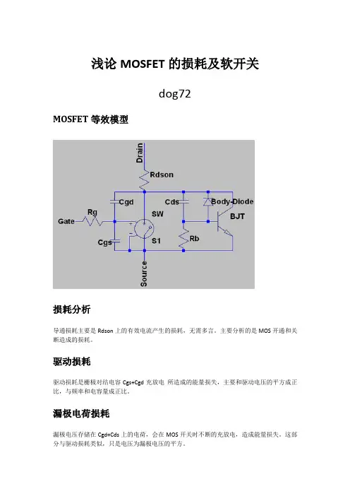
MOSFET损耗分析
- 格式:pdf
- 大小:317.99 KB
- 文档页数:18
APPENDIX AEstimating MOSFET Parameters from the Data Sheet(Equivalent Capacitances, Gate Charge, Gate Threshold Voltage,Miller Plateau Voltage, Internal Gate Resistance, Maximum Dv/Dt)In this example, the equivalent C GS , C GD , and C DS capacitances, total gate charge, the gate threshold voltage and Miller plateau voltage, approximate internal gate resistance, and dv/dt limits of an IRFP450MOSFET will be calculated. A representative diagram of the device in a ground referenced gate drive application is pictured below.V The following application information are given to carry out the necessary calculations:V DS,OFF =380V the nominal drain-to-source off state voltage of the device.I D =5A the maximum drain current at full load.T J =100°C the operating junction temperature.V DRV =13V the amplitude of the gate drive waveform.R GATE =5Ωthe external gate resistance.R LO =R HI =5Ωthe output resistances of the gate driver circuit.A1.CapacitancesThe data sheet of the IRFP450 gives the following capacitance values:Using these values as a starting point, the average capacitances for the actual application can be estimated as:Equations:Numerical Example:offDS,spec DS,spec OSS,ave OSS,off DS,spec DS,spec RSS,ave RSS,V V C 2C V V C 2C ⋅⋅=⋅⋅=369pF 380V25V720pF 2C 174pF 380V 25V340pF 2C ave OSS,ave RSS,=⋅⋅==⋅⋅=The physical capacitor values can be obtained from the basic relationships:aveRSS,ave OSS,DS RSS ISS GS ave RSS,GD C C C C C C C C −=−==195pF174pF 369pF C 2260pF 340pF 2600pF C 174pFC DS GS GD =−==−==Notice that C GS is calculated from the original data sheet values. Within one equation, it is important to use capacitor values which are measured under the same test conditions. Also keep in mind that C GS is constant, it is not voltage dependent. On the other hand, C GD and C DS capacitors are strongly non-linear and voltage dependent. Their highest value is at or near 0V and rapidly decreasing as the voltage increases across the gate-to-drain and drain-to-source terminals respectively.A2.Gate chargeThe worst case gate charge numbers for a particular gate drive amplitude, drain current level, and drainoff state voltage are given in the IRFP450 data sheet.Correcting for a different gate drive amplitude is simple using the typical Total Gate Charge curve as illustrated on the left.Starting from the 13V gate-to-source voltage on the left hand side, find the corresponding drain-to-source voltage curve (interpolate if not given exactly), then read the total gate charge value on the horizontal axes.If a more accurate value is required, the different gate charge components must be determined individually. The gate-to-source charge can be estimated from the curve on the left, only the correct Miller plateau level must be known. The Miller charge can be calculated from the C RSS,AVE value obtained in A1. Finally, the over drive charge component – raising the gate-to-source voltage from the Miller plateau to the final amplitude – should be estimated from the graph on the left again.13V122nCA3.Gate threshold and Miller plateau voltagesAs it was already shown in A2, and will be demonstrated later, several MOSFET switching characteristic are influenced by the actual value of the gate threshold and Miller plateau voltages. In order to calculate the Miller plateau voltage, one possibility would be to use the gate-to-source threshold voltage (V TH ) and transconductance (g fs) of the MOSFET as listed in the data sheet.Unfortunately, the threshold is not very well defined and the listed g fs is a small signal quantity. A more accurate method to obtain the actual V TH and Miller plateau voltages is to use the Typical Transfer Characteristics curves of the data sheet.From the same temperature curve, pick two easy to read points and note the corresponding drain currents and gate-to-source voltages. Select the drain current values to correspond to vertical grid lines of the graph, that way the currents can be read accurately. Then follow the intersections to the horizontal axes and read the gate-to-source voltages.Starting with the drain currents will result in higher accuracy because the gate-to-source voltage is on a linear scale as opposed to the logarithmic scale in drain current. It is easier to estimate Vgs1 and Vgs2on the linear scale therefore the potential errors are much smaller.For this example, using the 150°C curve:5.67VV 20A I 4.13V V 3A I GS2D2GS1D1====The gate threshold and Miller Plateau voltages can be calculated as:()()()KI V V V V I K I I I V I V V V V K I V V K I LOADTHMiller GS,2TH GS1D1D1D2D1GS2D2GS1TH 2TH GS2D22TH GS1D1+=−=−⋅−⋅=−⋅=−⋅=() 4.413V 3.1695A3.157V V 3.1693.157V4.13V 3AK 3.157V3A 20A 3A5.67V 20A 4.13V V Miller GS,2TH =+==−==−⋅−⋅=I D1I D2V GS1V GS2Typical Transfer CharacteristicsThese values correspond to 150°C junction temperature, because the 150°C curve from the Typical Transfer Characteristics was used. Due to the substantial temperature coefficient of the threshold voltage, the results have to be corrected for the 100°C operating junction temperature in this application.The gate threshold voltage and the Miller plateau voltage level must be adjusted by:()TCC 150T ∆V J ADJ ⋅°−=()0.35VC V 0.007C 150C 100∆V ADJ +=÷øöçèæ°−⋅°−°=A4.Internal gate resistanceAnother interesting parameter is the internal gate mesh resistance (R G,I ), which is not defined in the data sheet. This resistance is an equivalent value of a distributed resistor network connecting the gates of the individual MOSFET transistor cells in the device. Consequently, the gate signal distribution within a device looks and behaves very similar to a transmission line. This results in different switching times of the individual MOSFET cells within a device depending on the cells distance from the bound pad of the gate connection.The most reliable method to determine R G,I is to measure it with an impedance bridge. The measurement is identical to the ESR measurement of capacitors which is routinely carried out in the lab. For this measurement the source and drain terminals of the MOSFET are shorted together. The impedance analyzer should be set to R S -C S or if it is available R S -C S -L S equivalent circuit to yield the component values of the equivalent gate resistor, R G,I , the MOSFET’s input capacitance, C ISS and the series parasitic inductance of the device, all connected in series.For this example, the equivalent component values of an IRFP450 were measured by an HP4194impedance analyzer. The internal gate resistance of the device was determined as R G,I =1.6Ω. The equivalent inductance was measured at 12.9nH and the input capacitance was 5.85nF.A5.dv/dt limitMOSFET transistors are susceptible to dv/dt induced turn-on only when their drain-to-source voltage rises rapidly. Fundamentally, the turn-on is caused by the current flowing through the gate-drain capacitor of the device and generating a positive gate-to-source voltage. When the amplitude of this voltage exceeds the gate-to-source turn-on threshold of the device, the MOSFET starts to turn-on. There are three different scenarios to consider.First, look at the capacitive divider formed by the C GD and C GS capacitors. Based on these capacitor values the gate-to-source voltage can be calculated as:GD GS GDDS GS C C C V V +⋅=If V GS <V TH , the MOSFET stays off. The maximum drain-to-source voltage to ensure this can be estimated by:GDGDGSTH MAX DS,C C C V V +⋅≈This mechanism provides full protection against dv/dt induced turn-on in low voltage applications,independent of the internal gate resistor and the external drive impedances.For higher voltage applications, it is desirable to determine the natural dv/dt limit of the MOSFET. This characteristic corresponds to the maximum dv/dt the device can withstand without turning on in an ideal situation where the external drive impedance is zero. This is signified by the shorted gate-source connection in the schematic diagram on the right.The turn-on is initiated by the voltage dropacross R G,I due to the charge current of C GD .Accordingly, the natural dv/dt limit can be calculated by:GDI G,TH LIMIT -N C R V dt dv⋅=This number is significant in evaluating the suitability of a device for a specific application where the turn-off dv/dt is forced by other components in the circuit. These applications include synchronous rectifiers, resonant mode and soft-switching power converters.The third calculation describes the resulting dv/dt limit of the drain-to-source voltage waveform based on the parasitic components of the MOSFET device and the characteristics of the gate drive circuit.To avoid turn-on, the gate-to-source voltage must stay below the turn-on threshold voltage:()GDLO GATE I G,TH LIMIT C R R R V dt dv⋅++=It is important to emphasize again that the threshold voltage of the MOSFET transistor changes significantly with temperature. Therefore, the effect of high junction temperature must be taken into effect. For the particular example using the IRFP450 type transistor at 100°C operating junction temperature the calculations yield the following limitations:Case 1. No dv/dt induced turn-on takes place below the drain-to-source voltage of:()GD GD GSADJ TH MAX DS,C C C ∆V V V +⋅+=()26.82V 340pF 2600pF0.35V 3.157V V MAX DS,=⋅+=Case 2. The natural dv/dt limit of the IRFP450 is:GDI G,ADJ THLIMIT -N C R ∆V V dt dv⋅+=µskV6.4340pF 1.6Ω0.35V 3.157V dt dv LIMIT -N =⋅+=Case 3. The in-circuit dv/dt limit including the effect of the driver’s output impedance is:()GD LO GATE I G,ADJ TH LIMIT C R R R ∆V V dt dv ⋅+++=()µsV889340pF 5Ω5Ω1.6Ω0.35V 3.157V dt dv LIMIT =⋅+++=Calculating Driver Bypass Capacitor ValueMOSFET drivers must be operated from a low impedance voltage source to achieve high switching speed and reliable operation. To provide this virtual voltage source, the bias line of the drivers must be locally bypassed by very good quality, high frequency capacitors. In most applications this capacitance is realized by low impedance, high frequency, multilayer ceramic capacitors. Half of the success in bypassing can be ensured by the proper location of the bypass capacitors and the driver itself. Some of the most important rules of proper gate drive design are highlighted in the example below:• The driver should be close to the device it is driving. Significant distance can be tolerated between the PWM controller and the MOSFET driver with careful layout design. Even though there is no high current between the output of the PWM IC and the input of the driver, relatively wide printed circuit board traces can reduce the parasitic interconnection inductance, thus providing lower loop impedance and better noise immunity.• It is also important to separately bypass the individual noise sources, i.e. the power stage, the PWM controller and the driver both have their own respective bypass capacitors. The three shaded loop areas must be minimized.During turn-on the gate current flows through the bypass capacitor of the driver, while during turn-off the high frequency bypass capacitor of the power stage must provide a path to charge the C GD capacitor of the MOSFET.In this numerical example an IRFP350 MOSFET is driven by a Micrel MIC4423 driver. The driver’s quiescent current I Q,HI with a high input, is 2.5mA. When the input is low the quiescent current is negligible. The switching frequency is 100kHz and the maximum duty ratio of the PWM signal is 0.7.The gate is driven by a 12V signal, and the off state voltage of the device is approximately 300V.From these operating conditions the total gate charge can be estimated as 115nC. A 5% percent ripple voltage across the bypass capacitor is acceptable, and a 12V bias would allow 0.6V ripple voltage. The equation to calculate the minimum bypass capacitor value is:∆V Q f D I C G DRV MAX HI Q,BYPASS +⋅=221nF 0.6V 115nC 100kHz 0.72.5mA C BYPASS =+⋅=The effect of switching frequency on the bypass capacitorvalue is depicted in the figure on the right. At high frequency,the gate charge determines the minimum bypass capacitor,thus the curve approaches an asymptotic minimum value. At low operating frequencies the quiescent current of the driver commands the minimum capacitor size. Note that this ripple component depends on the duty ratio of the PWM signal.For this calculation, the worst case situation (D=0.7) was considered.V IN1010010000.20.30.40.5Switching Frequency [kHz]M i n i m u m B y p a s s C a p a c i t o r [µF ]Bootstrap Bypass Capacitor ExampleIn this example an IR2125 high voltage integrated gate driver is employed to drive an IRF1310N transistor in a 48V input buck converter. The corresponding schematic diagram is given below.VV BIAS V OUT V DRV Let’s assume the following application parameters:V IN,MAX =65V the maximum steady state input voltage.V DRV =12V the bias voltage for the high side driver and the gate drive amplitude.∆V BST =0.5V the steady state ripple voltage across C BST .∆V BST,MAX =3V the maximum voltage droop across C BST before the driver goes to under voltage lockout or the gate drive amplitude becomes insufficient.f DRV =100kHz the switching frequency.D MAX =0.9the maximum steady state duty ratio at minimum input voltage – the controller does not limit the maximum duty cycle in this example.t OFF,TR =400µs transient off-time – at sudden removal of the load, the MOSFET stays off for this time interval.t ON,TR =200µstransient on-time – at sudden increase of the load current, the controller keeps the MOSFET on for this time interval to build up the output inductor current.The circuit components are characterized by:Q G =85nC the total gate charge of the IRF1310 @ V DRV =12V and V DS =65V.R GS =5.1k Ωthe gate-to-source pull down resistor value.I R =10µA leakage current of D BST @ V IN,MAX and T J =80°C.V F =0.6V forward voltage drop of D BST @ 0.1A and T J =80°C.I LK =0.13mA leakage current of the level shifter @ V IN,MAX and T J =100°C.I QBS =1mAquiescent current of the floating driver.First, consider the steady state operation of the driver. Based on the ripple budget of 0.5V and the amount of charge consumed from the bootstrap capacitor, a minimum capacitance value can be established:BSTG DRVMAX GS F DRV QBS LK R BST,1∆V Q f D R V V I I I C +⋅÷÷øöççèæ−+++=Substituting the numerical values yields the minimum bootstrap capacitor value for steady state operation:231nF 0.5V85nC 100kHz 0.95.1k Ω0.6V 12V 1mA 0.13mA A 10µC BST,1=+⋅÷øöçèæ−+++=For the transient conditions calculate the capacitor values based on the maximum voltage droop. When the switch has to stay off for an extended period of time, the output inductor current decays to zero and the source of the main switch settles at the output voltage. The bootstrap diode is reverse biased and the bootstrap capacitor has to keep the floating driver alive. Moreover, at the end of the idle period, C BST still has to provide the gate charge to turn-on the MOSFET. Accordingly, the required capacitor value is:MAXBST,GTR OFF,GS F DRV QBS LK R BST,2∆V Q t R V V I I I C +⋅÷÷øöççèæ−+++=Using the actual application parameters:nF478V3nC85µs 400k Ω1.5V 6.0V 12mA 1mA 13.0µA 10C 2BST,=+⋅÷øöçèæ−+++=The last calculation is carried out to check whether the switch can be turned on continuously for the desired 200 microseconds transient on time. The long on period will be followed by a guaranteed off-time when the bootstrap capacitor can be replenished. The bootstrap capacitor must hold enough energy to support the quiescent and leakage currents only as indicated in the expression below:MAXBST,TRON,GS F DRV QBS LK R BST,3∆V t R V V I I I C ⋅÷÷øöççèæ−+++=With the given numerical values:nF 225V3µs200k Ω1.5V 6.0V 12mA 1mA 13.0µA 10C 3BST,=⋅÷øöçèæ−+++=To fulfill all three requirements, the highest capacitor value (C BST =470nF) should be selected.The high side driver IC must be bypassed not only by the bootstrap capacitor, but also by another ground referenced capacitor as indicated in the schematic diagram. C DRV provides the high peak charge current to replenish the energy taken from C BST during the preceding on-time of the main MOSFET. If C DRV >> C BST , the bootstrap capacitor can be recharged to the full V DRV level. Usually, C DRV is an order of magnitude larger capacitance than C BST . When selecting the value of the low side bypass capacitor,primarily the steady state operation should be considered. Accordingly,BST,1DRV C 10C ⋅≈, which requires C DRV = 2.2µF.APPENDIX DCoupling Capacitor and Transient Settling Time CalculationIn this example the coupling capacitor and gate-to-source resistor value of an AC coupled gate drive circuit will be calculated. The design goal is to provide a 3V negative bias for the MOSFET during its off time. The application circuit is shown below:V DRV V INThe following application information is given:dV IN /dt=200V/ms the maximum dv/dt of the input voltage during power up, limited by the combined effect of the inrush current limiting circuit and the input energy storage capacitor.C GD,0=1nF the maximum gate-to-drain capacitance of the MOSFET read from the data sheet at 0V drain-to-source voltage (worst case start-up condition).V TH =2.7V the gate-to-source turn-on threshold @ T A,MAX .V DRV =15V the supply voltage of the PWM controller, i.e. the gate driver’s bias voltage.f DRV =100kHz the switching frequency.D MAX =0.8maximum duty ratio, limited by the PWM controller to reset the transformer.V CL =3V the negative bias amplitude.∆V C =1.5V maximum allowable ripple of the coupling capacitor.Q G =80nC total gate charge of the MOSFET .τ=100µstransient time constant for the coupling capacitor voltage (V C ). This is the start-up time constant as well to establish the initial value of V C .The design starts by determining the maximum value of the gate pull down resistor. During power-up,R GS must be low enough to keep the MOSFET off. When the voltage rises across the drain-source terminal, the C GD capacitor is charged and a current proportional to dV IN /dt flows through R GS . The MOSFET stays off if the voltage drop across R GS remains below the gate threshold. Therefore, the maximum allowable R GS value is:dtdV C V R INGD,0THMAX GS,⋅=13.5k ΩsV2000001nF 2.7V R MAX GS,=⋅=The next step is to find the common solution for the required time constant and ripple voltage. The two equations are:D(D)V D V f ∆V f Q C R C C DRV DRV C DRVG C GSC τττ⋅+⋅−⋅⋅⋅⋅=⋅=where V C (D) is the coupling capacitor voltage as a function of the duty ratio. The second equation can be evaluated right away since all parameters are defined. In general, V C (D)=D ⋅V DRV if the clamp circuit is not used, and the expression has a local maximum at D=0.5, which gives the minimum coupling capacitor value. In this application, the coupling capacitor voltage is limited to 3V by the zener clamp.Thus for D>0.2, the coupling capacitor voltage is constant, and V C =3V. Consequently, the maximum value of the second equation is not at D=0.5, but rather at the maximum duty cycle, D MAX .Before calculating C C , another important limitation should be pointed out. In order to arrive at a meaningful positive capacitor value, the denominator of the second equation must be positive which sets a limit on the transient time constant. This limit is:()DRVC C DRV MIN f ∆V (D)V VD τ⋅−⋅=This function has a maximum value at D=0.5 if the clamp circuit is not used. With the clamp circuit,D=D MAX will define the fastest possible transient response of the coupling capacitor voltage.Substituting the application parameters and using the appropriate equation for the clamp case yields the following values:()DRVC CL DRV MAX MIN f ∆V V VD τ⋅−⋅=()µs64kHz100V 5.1V 3V 158.0MIN τ=⋅−⋅=()CL DRV MAX DRV C DRVG C V V D f ∆V f Q C ττ−⋅−⋅⋅⋅⋅=()nF148V 3V 158.0kHz 100µs 100V 5.1kHz100µs 100nC 80C C =−⋅−⋅⋅⋅⋅=CGS C R τ=Ω675nF148µs100R GS ==These results are acceptable because τMIN <τ and R GS,MAX >R GS , therefore all conditions are met. The worst case power dissipation of R GS is 173mW at the maximum duty ratio of 0.8. If this value is not acceptable, selecting a longer time constant will increase the pull down resistor value. At the same time the power dissipation and the coupling capacitor value will decrease.The last calculation is to compute the bypass capacitor value. Assuming a maximum of 1V ripple on the bias rail (∆V DRV =1V) the following minimum bypass capacitance value will result:MAXDRVGS DRV CLDRV DRV G DRV D f R ∆V V V ∆V Q C ⋅⋅⋅−+=222nF 0.8100kHz675Ω1V 3V15V 1V 80nC C DRV =⋅⋅⋅−+=APPENDIX EGate Drive Transformer Design ExampleThe gate drive transformers for a phase shifted full-bridge converter will be designed according to the schematic diagram below:V INIn this example, the PWM controller has four high current output drivers on-board. The gate drive transformer design is based on the following application information:f CLOCK =400kHz the clock frequency.f DRV =200kHz the operating frequency of the gate drive transformers.D MAX =0.5maximum duty ratio of the gate drive transformer.V DRV =15Vthe bias voltage of the controller, which is also used to power the output drivers.The first task is to choose the core size. A seasoned designer can pick the right core for the first try based on previous experience. But even then, like all magnetics problem solving, the gate drive transformer design might require a couple of iterations. For this application a Ferroxcube RM5/I core was selected with no airgap. The preferred choice of material is 3C94 because it has the highest permeability and lowest loss at 200kHz from the available selection.Ae=24.8mm 2effective cross section area of the core.Ve=574mm 3effective volume of the core.B SAT =0.35T saturation flux density of the ferrite material @ 100°C.A L =2µH/turns 2equivalent inductance per turns square.B PEAK =0.1T peak flux density in steady state operation. Remember, that during transient operation the transformer’s flux can walk due to uneven duty cycles. Usually, a 3:1 margin is desirable.∆B=0.2Tpeak-to-peak flux density in steady state operation.Check the core loss under these conditions from the data sheet.P V =200kW/m 3effective volumetric power dissipation of 3C94 @ B PEAK =0.1T and 200kHz.(it is more meaningful to convert to 0.2mW/mm 3.)eV CORE V P P ⋅=115mW 574mm mmmW0.2P 33CORE =⋅=The power dissipation of the RM5/I core is 115mW which is acceptable. Next, calculate the primary number of turns according to:DRVe MAX DRV Pf A ∆B D V N ⋅⋅⋅=7.56200kHz24.8mm 0.2T 0.515V N 2P =⋅⋅⋅=turns The next higher full turn is selected, N P =8 turns. Since voltage scaling is not required in this gate drive transformer, the two secondary windings have 8 turns as well. In order to minimize leakage inductance and AC winding resistance, each winding should occupy a single layer only. The following data is needed to execute the winding design:W W =4.7mm the winding width from the data sheet of the coil former.MLT=24.9mmthe average length of turn also from the coil former data sheet.Considering that at the termination N+1 wires are side by side, the corresponding wire diameter is:1N W d P W W +=20.5mils 0.52mm 94.7mmd W ===The closest smaller diameter wire size according to the American Wire Gauge table is #25 and its characteristic data is:d W =0.0199mils heavy built (double isolated) nominal diameter. (0.0199mils=0.506mm)ρW =32.37Ω/1000ft.normalized wire resistance. (32.37Ω/1000ft =0.1062m Ω/mm)The DC winding resistance is:WP DC W,ρMLT N R ⋅⋅=21.2m Ωmmm Ω0.106224.9mm 8R DC W,=⋅⋅=Next, check the AC resistance based on Dowell’s curves according to the following steps:DRVPEN f 7.6D =cm017.02000006.7D PEN ==PEN WD d 0.83Q ⋅=2.470.17mm 0.506mm 0.83Q =⋅=Entering Dowell’s graph at Q=2.5, the single layer curve gives an R AC /R DC =3 ratio, thus the AC resistance of the winding is R AC =3⋅21.2m Ω=63.6m Ω, which is quite acceptable.The last step is to calculate the magnetizing inductance and current values:2L M N A L ⋅=µH 1288turnsµH 2L 22M =⋅=DRVM MAXDRV M P M,f L D V 212∆I I ⋅⋅⋅==mA 146kHz200µH 1285.0V 1521I M,P =⋅⋅⋅=3D I I MAXP M,RMS M,⋅=60mA 30.5146mA I RMS M,=⋅=Based on the RMS value of the magnetizing current, the wire loss is:AC 2RMS M,W R I P ⋅=0.2mW63.6m Ω(60mA)P 2W =⋅=This result demonstrates that power dissipation in the winding is not an issue in the gate drive transformer. The high magnetizing inductance and low winding resistance are the most critical design parameters to achieve low droop in the gate drive waveform. Also notice that copper loss is based purely on AC resistance, because in an ideal, steady state operation there is no DC current in the windings.Finally, the winding arrangement of the transformer is shown below. The primary is near the center post,then the low side, and the high side windings. All windings are in a single layer. The low side winding is utilized as a natural shield against parasitic capacitive currents between signal ground and the floatingcircuitry.APPENDIX FA Step by Step Design Example of a Ground Referenced and aFloating High Side Gate Driver for an Active Clamp Flyback ConverterThe gate drive design process begins AFTER the power stage is designed and the power components are selected. The simplified final schematic diagram of the active clamp flyback converter is shown below.DCRload85OhmsThe relevant operating parameters are:V DS1,off=V DS2,off=285V the off state drain-to-source voltage of Q1 and Q2. Both transistors areswitching between ground (0V) and V IN+V CLAMP.I D1=2.7A the peak drain current of Q1 at turn-off.T J=100°C the operating junction temperature of the devices.L R=14uH the resonant inductor of the active clamp flyback power stage.The specified driver output impedances and gate drive parameters of the UCC3580-4 are:OUT1OUT2V DRV=15V V DRV=15VD MAX1=0.7D MAX2=0.95f DRV=250kHz f DRV=250kHzR HI1=20ΩR HI2=33ΩR LO1=10ΩR LO2=33ΩThe estimated MOSFET parameters according to the operating junction temperature and based on the methods demonstrated in the previous Appendix’s are:IRFP350IRF740Q G1=135nC Q G2=60nC C GD1=148pF C GD2=71pF C OSS1=391pF C OSS2=195pF R G1,I =1.2ΩR G2,I =1.63ΩV TH1=3.2V V TH2=3.5V V GS1,Miller =4.2V V GS2,Miller =4.8VNext, establish the dv/dt of the external resonant circuit and the dv/dt of the devices. At node A, the resonant inductor, L R , charges and discharges the effective node capacitance. The inductor current barely changes during the short switching action, therefore it can be looked at as a DC current source.The node capacitance and the resulting dv/dt of the power stage are:RD1RES OSS2OSS1R C I dt dvC C C ≈+=µskV4.6586pF 2.7A dt dv 586pF 195pF 391pF C RES R =≈=+=The turn-on dv/dt of the MOSFET and the dv/dt LIMIT to prevent dv/dt induced turn-on assumingR GATE =0Ω are:()GD HI I G,Miller GS,DRV ON C R R V V dt dv ⋅+−=()µs kV 3.4148pF20Ω1.2Ω 4.2V 15V dt dv ON Q1,=⋅+−=()µs kV 4.1571pF33Ω1.63Ω 4.8V15V dt dv ON Q2,=⋅+−=()GDLO I G,TH LIMIT C R R V dt dv⋅+=()µs kV 1.93148pF10Ω1.2Ω 3.2Vdt dv LIMIT Q1,=⋅+=()µs kV 1.421pF733Ω1.63Ω3.5Vdt dv LIMIT Q2,=⋅+=Since the resonant dv/dt is higher than the dv/dt LIMIT calculated for both Q1 and Q2 transistors, a turn-off speed-up circuit must be used in both drive circuits. The selected low side and high side gate drivecircuits are presented below:IRFP350(Low Side Drive)IRF740(High Side Drive)Now, the dv/dt LIMIT numbers must be re-calculated assuming that the drivers’ output impedance is shunted out. Also, pay attention to the 0.7V voltage drop across the pn junction of the Q OFF transistors.µs kV 14148pF 2.10.7V -3.2V dt dv LIMIT Q1,=⋅Ω=µs kV 241pF71.63Ω0.7V-3.5V dt dv LIMIT Q2,=⋅=。