lm339完整资料
- 格式:pdf
- 大小:1.20 MB
- 文档页数:33
四电压比较器LM339简介LM339集成块内部装有四个独立的电压比较器,该电压比较器的特点是:1)失调电压小,典型值为2mV;2)电源电压范围宽,单电源为2-36V,双电源电压为±1V-±18V;3)对比较信号源的内阻限制较宽;4)共模范围很大,为0~(Ucc-1.5V)V o;5)差动输入电压范围较大,大到可以等于电源电压;6)输出端电位可灵活方便地选用。
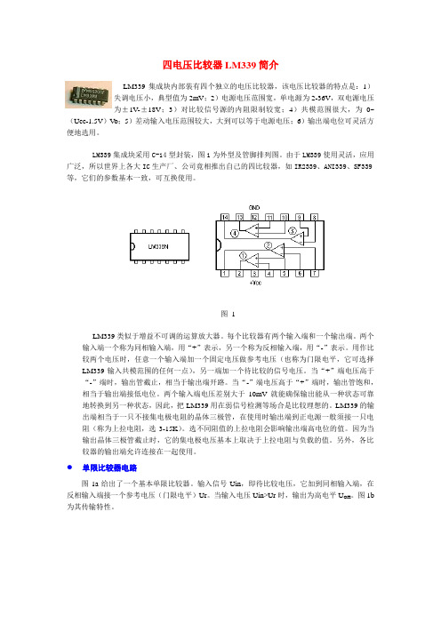
LM339集成块采用C-14型封装,图1为外型及管脚排列图。
由于LM339使用灵活,应用广泛,所以世界上各大IC生产厂、公司竟相推出自己的四比较器,如IR2339、ANI339、SF339等,它们的参数基本一致,可互换使用。
图 1LM339类似于增益不可调的运算放大器。
每个比较器有两个输入端和一个输出端。
两个输入端一个称为同相输入端,用“+”表示,另一个称为反相输入端,用“-”表示。
用作比较两个电压时,任意一个输入端加一个固定电压做参考电压(也称为门限电平,它可选择LM339输入共模范围的任何一点),另一端加一个待比较的信号电压。
当“+”端电压高于“-”端时,输出管截止,相当于输出端开路。
当“-”端电压高于“+”端时,输出管饱和,相当于输出端接低电位。
两个输入端电压差别大于10mV就能确保输出能从一种状态可靠地转换到另一种状态,因此,把LM339用在弱信号检测等场合是比较理想的。
LM339的输出端相当于一只不接集电极电阻的晶体三极管,在使用时输出端到正电源一般须接一只电阻(称为上拉电阻,选3-15K)。
选不同阻值的上拉电阻会影响输出端高电位的值。
因为当输出晶体三极管截止时,它的集电极电压基本上取决于上拉电阻与负载的值。
另外,各比较器的输出端允许连接在一起使用。
单限比较器电路图1a给出了一个基本单限比较器。
输入信号Uin,即待比较电压,它加到同相输入端,在反相输入端接一个参考电压(门限电平)Ur。
当输入电压Uin>Ur时,输出为高电平U OH。

四电压比较器LM339简介LM339集成块内部装有四个独立的电压比较器,该电压比较器的特点是:1)失调电压小,典型值为2mV;2)电源电压范围宽,单电源为2-36V,双电源电压为±1V-±18V;3)对比较信号源的内阻限制较宽;4)共模范围很大,为0~(Ucc-1.5V)V o;5)差动输入电压范围较大,大到可以等于电源电压;6)输出端电位可灵活方便地选用。
LM339集成块采用C-14型封装,图1为外型及管脚排列图。
由于LM339使用灵活,应用广泛,所以世界上各大IC生产厂、公司竟相推出自己的四比较器,如IR2339、ANI339、SF339等,它们的参数基本一致,可互换使用。
图1LM339类似于增益不可调的运算放大器。
每个比较器有两个输入端和一个输出端。
两个输入端一个称为同相输入端,用“+”表示,另一个称为反相输入端,用“-”表示。
用作比较两个电压时,任意一个输入端加一个固定电压做参考电压(也称为门限电平,它可选择LM339输入共模范围的任何一点),另一端加一个待比较的信号电压。
当“+”端电压高于“-”端时,输出管截止,相当于输出端开路。
当“-”端电压高于“+”端时,输出管饱和,相当于输出端接低电位。
两个输入端电压差别大于10mV就能确保输出能从一种状态可靠地转换到另一种状态,因此,把LM339用在弱信号检测等场合是比较理想的。
LM339的输出端相当于一只不接集电极电阻的晶体三极管,在使用时输出端到正电源一般须接一只电阻(称为上拉电阻,选3-15K)。
选不同阻值的上拉电阻会影响输出端高电位的值。
因为当输出晶体三极管截止时,它的集电极电压基本上取决于上拉电阻与负载的值。
另外,各比较器的输出端允许连接在一起使用。
单限比较器电路图1a给出了一个基本单限比较器。
输入信号Uin,即待比较电压,它加到同相输入端,在反相输入端接一个参考电压(门限电平)Ur。
当输入电压Uin>Ur时,输出为高电平U OH。
LM339/LM393中文资料及PDF下载什么是lm339LM339/LM393是四电压比较器集成电路。
由于LM339 使用灵活,应用广泛,所以世界上各大IC 生产厂、公司竟相推出自己的四比较器,如IR2339、ANI339、SF339 等,它们的参数基本一致,可互换使用。
LM339 类似于增益不可调的运算放大器。
每个比较器有两个输入端和一个输出端。
两个输入端一个称为同相输入端,用“+”表示,另一个称为反相输入端,用“-”表示。
用作比较两个电压时,任意一个输入端加一个固定电压做参考电压(也称为门限电平,它可选择LM339 输入共模范围的任何一点),另一端加一个待比较的信号电压。
当“+”端电压高于“-”端时,输出管截止,相当于输出端开路。
当“-”端电压高于“+”端时,输出管饱和,相当于输出端接低电位。
两个输入端电压差别大于10mV 就能确保输出能从一种状态可靠地转换到另一种状态,因此,把LM339 用在弱信号检测等场合是比较理想的。
LM339 的输出端相当于一只不接集电极电阻的晶体三极管,在使用时输出端到正电源一般须接一只电阻(称为上拉电阻,选3-15K)。
选不同阻值的上拉电阻会影响输出端高电位的值。
因为当输出晶体三极管截止时,它的集电极电压基本上取决于上拉电阻与负载的值。
另外,各比较器的输出端允许连接在一起使用。
�8�5 图1a 给出了一个基本单限比较器。
输入信号Uin,即待比较电压,它加到同相输入端,在反相输入端接一个参考电压(门限电平)Ur。
当输入电压Uin>Ur 时,输出为高电平U OH 。
该电路的特点如下:1 .工作电源电压范围宽,单电源、双电源均可工作,单电源:2~36V,双电源:±1~±18V;2. 消耗电流小,Icc=1.3mA;3. 输入失调电压小,VIO=±2mV;ab126计算公式大全4. 共模输入电压范围宽,Vic=0~Vcc-1.5V;5. 对比较信号源的内阻限制较宽;6. 输出与TTL,DTL,MOS,CMOS 等兼容;7. 输出可以用开路集电极连接“或”门;8. 采用双列直插14引脚塑料封装(DIP14)和微形的双列14脚塑料封装(SOP14)内部结构图及引脚图功能排列表引脚功能符号引引脚功能符号1 输出端2 OUT2 8 反向输入端31N-(3)2 输出端1OUT1 9正向输入端31N+(3)3 电源VCC + 10反向输入端41N-(4)4 反向输入端11N-(1) 11正向输入端41N+(4)5 正向输入端1 1N+(1) 12电源Vcc-6 反向输入端2 1N-(2) 13输出端4 OUT47 正向输入端2OUT2(2) 14输出端3 OUT3LM339主要参数表:参数名称符号数值单位电源电压 VCC ±18 或36 V 差模输入电压 VID ±36 V 共模输入电压 VI -0.3~VCC V 功耗Pd 570 mW 工作环境温度 Topr 0 to +70 ℃贮存温度Tstg -65 to 150 ℃ 电特性(除非特别说明,VCC=5.0V,Tamb=25℃)数名称符号测试条件最小典型最大单位输入失调电压VIOVCM=0 toVCC-1.5VO(P)=1.4V, Rs=0-±1.0 ±5.0 mV输入失调电流IIO --±5 ±50 nA输入偏置电流Ib--65 250 nA共模输入电压VIC -0 -VCC-1.5 V 静态电流ICCVCC = +5V, noload- 1.1 2.0 mA VCC = +30V, noload- 1.3 2.5 mA电A V -200 -V/mV压增益灌电流lsinkVi(-)>1V,Vi(+)=0V, V o(p)<1.5V6 16 -mA输出漏电流IOLEVi(-)=0V,Vi(+)=1V, VO=5V-0.1 -nALM339/LM393中文资料及PDF下载http://www.originic.hk/Item/Show.asp?m=1&d=1566。

lm339中文资料及电路LM339是一种广泛应用于电子电路中的比较器芯片,具有高精度、低功耗和高速度的特点。
在各种电子设备中,我们经常会用到比较器来判断电压信号的大小关系,而LM339正是一种常用的比较器芯片。
我们先来了解一下LM339芯片的基本结构和特性。
LM339芯片由四个独立的比较器组成,它们分别是A、B、C和D。
每个比较器都有一个非常重要的参数,即输入阈值电压。
当输入电压超过这个阈值时,比较器的输出会发生变化。
这个阈值电压可以通过外部电阻和电源电压进行调节,从而实现对比较器的输入灵敏度的控制。
在实际应用中,我们可以通过将待比较的电压信号分别接到比较器的两个输入端,然后根据比较器的输出来判断电压的大小关系。
比如,当A输入端的电压高于B输入端的电压时,A输出端为高电平,B输出端为低电平。
反之,当A输入端的电压低于B输入端的电压时,A输出端为低电平,B输出端为高电平。
这样,我们就可以根据比较器的输出来判断两个电压信号的大小关系。
除了基本的比较功能之外,LM339芯片还具有一些其他的特性。
首先,它的供电电压范围比较宽,通常可以达到2V至36V。
这使得LM339芯片在不同的电源电压条件下都能正常工作。
其次,它的输出电流较大,可以达到16mA,这样可以直接驱动一些负载电阻。
此外,LM339芯片的工作温度范围也相对较广,通常可以达到-40℃至+125℃,适用于各种环境条件。
在实际的电子电路设计中,我们常常需要使用到LM339芯片。
以电压比较为例,我们可以利用LM339芯片来实现电压的过高或过低检测。
比如,在一个温度控制系统中,我们可以将温度传感器的输出电压与设定的阈值电压进行比较,从而判断当前的温度是否在设定范围内。
如果温度过高或过低,LM339芯片就会产生相应的输出信号,我们可以利用这个信号来控制一些外部设备,如通风装置或加热器,实现温度的自动控制。
除了电压比较外,LM339芯片还可以应用于许多其他领域。
USA/EUROPE Literature Fulfillment :Literature Distribution Center for ON Semiconductor P .O. Box 5163, Denver, Colorado 80217 USAPhone : 303–675–2175 or 800–344–3860 Toll Free USA/Canada Fax : 303–675–2176 or 800–344–3867 Toll Free USA/Canada Email : ONlit@Fax Response Line *:303–675–2167800–344–3810 Toll Free USA/Canada*To receive a Fax of our publicationsON Semiconductor and are trademarks of Semiconductor Components Industries, LLC (SCILLC). SCILLC reserves the right to make changes without further notice to any products herein. SCILLC makes no warranty, representation or guarantee regarding the suitability of its products for any particular purpose, nor does SCILLC assume any liability arising out of the application or use of any product or circuit, and specifically disclaims any and all liability,including without limitation special, consequential or incidental damages. “Typical” parameters which may be provided in SCILLC data sheets and/or specifications can and do vary in different applications and actual performance may vary over time. All operating parameters, including “Typicals” must be validated for each customer application by customer’s technical experts. SCILLC does not convey any license under its patent rights nor the rights of others.SCILLC products are not designed, intended, or authorized for use as components in systems intended for surgical implant into the body, or other applications intended to support or sustain life, or for any other application in which the failure of the SCILLC product could create a situation where personal injury or death may occur. Should Buyer purchase or use SCILLC products for any such unintended or unauthorized application, Buyer shall indemnify and hold SCILLC and its officers, employees, subsidiaries, affiliates, and distributors harmless against all claims, costs, damages, and expenses, and reasonable attorney fees arising out of, directly or indirectly, any claim of personal injury or death associated with such unintended or unauthorized use, even if such claim alleges that SCILLC was negligent regarding the design or manufacture of the part. SCILLC is an Equal Opportunity/Affirmative Action Employer.PUBLICATION ORDERING INFORMATIONASIA/PACIFIC : LDC for ON Semiconductor – Asia SupportPhone :303–675–2121 (Tue–Fri 9:00am to 1:00pm, Hong Kong Time)Email : ONlit–asia@JAPAN : ON Semiconductor, Japan Customer Focus Center4–32–1 Nishi–Gotanda, Shinagawa–ku, Tokyo, Japan 141–8549Phone : 81–3–5487–8345Email : r14153@ON Semiconductor Website: 。
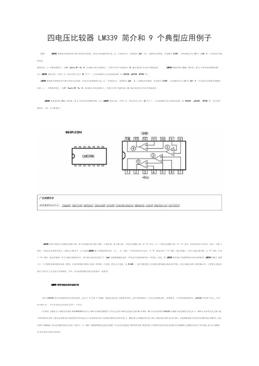
四电压比较器 LM339 简介和 9 个典型应用例子摘要:LM339 集成块内部装有四个独立的电压比较器,该电压比较器的特点是:1 )失调电压小,典型值为 2mV ;2 )电源电压范围宽,单电源为 2-36V ,双电源电压为±1V - ±18V;3 )对比较信号源的内阻限制较宽;4)共模范围很大,为0~(Ucc-1.5V)Vo;5)差动输入电压范围较大,大到可以等于电源电压;6)输出端电位可灵活方便地选用。
LM339集成块采用 C-14 型封装,图 1 为外型及管脚排列图。
由于LM339 使用灵活,应用广泛,所以世界上各大 IC 生产厂、公司竟相推出自己的四比较器,如 IR2339、ANI339、SF339 等..LM339 集成块内部装有四个独立的电压比较器,该电压比较器的特点是:1 )失调电压小,典型值为 2mV ;2 )电源电压范围宽,单电源为 2-36V ,双电源电压为±1V -±18V;3 )对比较信号源的内阻限制较宽;4 )共模范围很大,为0~(Ucc-1.5V)Vo;5)差动输入电压范围较大,大到可以等于电源电压;6)输出端电位可灵活方便地选用。
LM339 集成块采用 C-14 型封装,图 1 为外型及管脚排列图。
由于LM339 使用灵活,应用广泛,所以世界上各大 IC 生产厂、公司竟相推出自己的四比较器,如 IR2339 、ANI339 、SF339 等,它们的参数基本一致,可互换使用。
LM339 类似于增益不可调的运算放大器。
每个比较器有两个输入端和一个输出端。
两个输入端一个称为同相输入端,用“+”表示,另一个称为反相输入端,用“ -”表示。
用作比较两个电压时,任意一个输入端加一个固定电压做参考电压(也称为门限电平,它可选择LM339输入共模范围的任何一点),另一端加一个待比较的信号电压。
当“+”端电压高于“-”端时,输出管截止,相当于输出端开路。
LM339 双极型线性集成电路
摘自—第一价值网(IC网络超市)
四差分比较器
1.LM339/E内部包括有四个独立的电压比较器
在很宽的电源电压范围内适用于双电源工作模式,
也适用于单电源工作模式.它的使用范围包括方波发生
器、时间延长器、脉冲发生器、多谐振荡器、高压数字逻
辑门、A/D转换器和MOS时钟驱动器等。
2.LM339/E的封装形式为14引线双列塑封直插式
特点:
★单或双电源工作模式
★电源电压范围宽:单电源(2—36V); 双电源(±1—±18V)
★低功耗电流,典型值为800μA
★开路集电极输出,便于线连
★输入偏置电流小,典型值为25nA
★输入失调电流小,典型值为±2.3nA
★输入失调电压小,典型值为±1.4mV
★共模输入电压范围宽,包括接地
★输出饱和压降小
★输出能与TTL、DTL和MOS逻辑系统相匹配
内部电路图
极限参数
第一价值网为您提供最低廉的价格,保证您最好的品质! LM339PDF资料下载/查看。
LM339中文资料lm339中文资料什么是lm339?LM339/LM393是四电压比较器集成电路。
该电路的特点如下:工作电源电压范围宽,单电源、双电源均可工作,单电源:2~36V,双电源:±1~±18V;消耗电流小,Icc=1.3mA;输入失调电压小,V IO=±2mV;共模输入电压范围宽,Vic=0~Vcc-1.5V;输出与TTL,DTL,MOS,CMOS 等兼容;输出可以用开路集电极连接“或”门;采用双列直插14 脚塑料封装(DIP14)和微形的双列14 脚塑料封装(SOP14)内部结构图1/4 的内部电路图LM339引脚功能排列表:引脚功能符号引引脚功能符号1 输出端2 OUT2 8 反向输入端31N-(3)2 输出端1OUT1 9正向输入端31N+(3)3 电源VCC + 10反向输入端41N-(4)4 反向输入端11N-(1) 11正向输入端41N+(4)5 正向输入端1 1N+(1) 12电源Vcc-6 反向输入端2 1N-(2) 13输出端4 OUT47 正向输入端2OUT2(2) 14输出端3 OUT3LM339主要参数表:参数名称符号数值单位电源电压VCC ±18 或36 V差模输入电压VID ±36 V共模输入电压VI -0.3~VCC V功耗Pd 570 mW工作环境温度Topr 0 to +70 ℃贮存温度Tstg -65 to 150 ℃电特性(除非特别说明,VCC=5.0V,Tamb=25℃)数名称符号测试条件最小典型最大单位输入失调电压VIO VCM=0 to VCC-1.5 VO(P)=1.4V,Rs=0-±1.0 ±5.0 mV输入失调电流IIO --±5 ±50 nA输入偏置电流Ib--65 250 nA共模输入电压VIC -0 -VCC-1.5 VVCC = +5V, no load - 1.1 2.0 mA 静态电流ICCVCC = +30V, no load- 1.3 2.5 mA 电压增益AV VCC=15V, RL>15kΩ-200 -V/mV 灌电流lsink Vi(-)>1V, Vi(+)=0V, Vo(p)<1.5V 6 16 -mA 输出漏电流IOLE Vi(-)=0V, Vi(+)=1V, VO=5V -0.1 -nA使用说明:LM393/339是高增益,宽频带器件,象大多数比较器一样,如果输出端到输入端有寄生电容而产生耦合,则很容易产生振荡.这种现象仅仅出现在当比较器改变状态时,输出电压过渡的间隙.电源加旁路滤波并不能解决这个问题,标准PC板的设计对减小输入—输出寄生电容耦合是有助的.减小输入电阻至小于10K将减小反馈信号,而且增加甚至很小的正反馈量(滞回1.0~10mV)能导致快速转换,使得不可能产生由于寄生电容引起的振荡.除非利用滞后,否则直接插入IC并在引脚上加上电阻将引起输入—输出在很短的转换周期内振荡,如果输入信号是脉冲波形,并且上升和下降时间相当快,则滞回将不需要.比较器的所有没有用的引脚必须接地.LM393/339偏置网络确立了其静态电流与电源电压范围2.0~30V无关.通常电源不需要加旁路电容。
LM339中文资料1. 简介LM339是一种通用比较器(comparator),由Texas Instruments(TI)公司生产。
它是一款低功耗、高精度、高速度的集成电路,适用于电压比较和电压测量等应用。
LM339内部集成了四个电压比较器,每个比较器都具有两个输入端和一个输出端,并且可以独立设置电源电压。
2. LM339的特性2.1 低功耗LM339采用了低功耗设计,工作电流仅为1.3mA。
它适用于电池供电和功耗敏感的应用。
2.2 高精度LM339具有高精度的比较能力,其输入偏置电流仅为25nA,输入偏置电压仅为5mV。
这使得LM339可以在对精度要求较高的应用中使用,如电压测量和自动控制等。
2.3 高速度LM339具有快速的响应速度,其响应时间为1μs。
这使得LM339可以在需要高速比较的应用中使用,如开关电路和信号处理等。
2.4 宽电源电压范围LM339的电源电压范围广,可以接受单一供电或双供电。
单一供电时,其工作范围为2V至36V;双供电时,其工作范围为±1V至±18V。
这使得LM339适用于各种供电系统和应用场景。
2.5 开关速度快LM339的开关速度快,可以在约30nS的时间内完成比较操作。
这使得LM339适用于高频率信号处理和数字电路。
3. LM339的应用3.1 电压比较由于LM339是一种比较器,其主要应用是进行电压比较。
通过调整输入电压和参考电压,可以判断两个电压的大小关系,并通过输出端的电平状态表示。
3.2 开关电路由于LM339的快速开关速度和高精度的比较能力,它可以用于开关电路,如电源切换、开关控制等。
通过比较输入电压和参考电压,可以控制开关的状态。
3.3 电压测量由于LM339具有高精度和低功耗的特点,可以用于电压测量和监测。
通过将待测电压与参考电压进行比较,可以得到准确的电压值。
3.4 自动控制LM339的高精度和高速度使其非常适合于自动控制系统。
LM139/LM239/LM339/LM2901/LM3302Low Power Low Offset Voltage Quad ComparatorsGeneral DescriptionThe LM139series consists of four independent precision voltage comparators with an offset voltage specification as low as 2mV max for all four comparators.These were de-signed specifically to operate from a single power supply over a wide range of voltages.Operation from split power supplies is also possible and the low power supply current drain is independent of the magnitude of the power supply voltage.These comparators also have a unique characteris-tic in that the input common-mode voltage range includes ground,even though operated from a single power supply voltage.Application areas include limit comparators,simple analog to digital converters;pulse,squarewave and time delay gen-erators;wide range VCO;MOS clock timers;multivibrators and high voltage digital logic gates.The LM139series was designed to directly interface with TTL and CMOS.When op-erated from both plus and minus power supplies,they will di-rectly interface with MOS logic —where the low power drain of the LM339is a distinct advantage over standard compara-tors.Advantagesn High precision comparatorsn Reduced V OS drift over temperature n Eliminates need for dual supplies n Allows sensing near GNDn Compatible with all forms of logicnPower drain suitable for battery operationFeaturesn Wide supply voltage range—LM139/139A Series 2to 36V DC or ±1to ±18V DC —LM2901:2to 36V DC or ±1to ±18V DC —LM3302:2to 28V DC or ±1to ±14V DC n Very low supply current drain (0.8mA)—independent of supply voltagen Low input biasing current:25nAn Low input offset current:±5nA n Offset voltage:±3mV n Input common-mode voltage range includes GND n Differential input voltage range equal to the power supply voltagen Low output saturation voltage:250mV at 4mA n Output voltage compatible with TTL,DTL,ECL,MOS and CMOS logic systemsConnection DiagramsDS005706-27Order Number LM139AW/883or LM139W/883(Note 1)LM139AWRQML and LM139AWRQMLV (Note 3)See NS Package Number W14BLM139AWGRQML and LM139AWGRQMLV (Note 3)See NS Package Number WG14ANovember 1999LM139/LM239/LM339/LM2901/LM3302Low Power Low Offset Voltage Quad Comparators©1999National Semiconductor Corporation Connection Diagrams(Continued)Note 1:Available per JM38510/11201Note 2:Available per SMD #5962-8873901Note 3:See STD Mil Dwg 5962R96738for Radiation Tolerant DeviceDual-In-Line PackageDS005706-2Order Number LM139J,LM139J/883(Note 1),LM139AJ,LM139AJ/883(Note 2),LM239J,LM239AJ,LM339J,LM139AJRQML and LM139AJRQMLV (Note 3)See NS Package Number J14AOrder Number LM339AM,LM339M or LM2901MSee NS Package Number M14AOrder Number LM339N,LM339AN,LM2901N or LM3302NSee NS Package Number N14AL M 139/L M 239/L M 339/L M 2901/L M 3302 2LM139/LM239/LM339/LM2901/LM3302 Absolute Maximum Ratings(Note13)If Military/Aerospace specified devices are required,please contact the National Semiconductor Sales Office/ Distributors for availability and specifications.LM139/LM239/LM339LM139A/LM239A/LM339A LM3302LM2901Supply Voltage,V+36V DC or±18V DC28V DC or±14V DC Differential Input Voltage(Note11)36V DC28V DCInput Voltage−0.3V DC to+36V DC−0.3V DC to+28V DCInput Current(V IN<−0.3V DC),(Note6)50mA50mAPower Dissipation(Note4)Molded DIP1050mW1050mWCavity DIP1190mWSmall Outline Package760mWOutput Short-Circuit to GND,(Note5)Continuous ContinuousStorage Temperature Range−65˚C to+150˚C−65˚C to+150˚CLead Temperature(Soldering,10seconds)260˚C260˚COperating Temperature Range−40˚C to+85˚CLM339/LM339A0˚C to+70˚CLM239/LM239A−25˚C to+85˚CLM2901−40˚C to+85˚CLM139/LM139A−55˚C to+125˚CSoldering InformationDual-In-Line PackageSoldering(10seconds)260˚C260˚CSmall Outline PackageVapor Phase(60seconds)215˚C215˚CInfrared(15seconds)220˚C220˚CSee AN-450“Surface Mounting Methods and Their Effect on Product Reliability”for other methods of soldering surface mount devices.ESD rating(1.5kΩin series with100pF)600V600VElectrical Characteristics(V+=5V DC,T A=25˚C,unless otherwise stated)Parameter Conditions LM139A LM239A,LM339A LM139UnitsMin Typ Max Min Typ Max Min Typ MaxInput Offset Voltage(Note12) 1.0 2.0 1.0 2.0 2.0 5.0mV DCInput Bias Current I IN(+)or I IN(−)with Output in251002525025100nA DCLinear Range,(Note8),V CM=0VInput Offset Current I IN(+)−I IN(−),V CM=0V 3.025 5.050 3.025nA DCInput Common-Mode V+=30V DC(LM3302,0V+−1.50V+−1.50V+−1.5V DCVoltage Range V+=28V DC)(Note9)Supply Current R L=∞on all Comparators,0.8 2.00.8 2.00.8 2.0mA DC R L=∞,V+=36V, 1.0 2.5 1.0 2.5mA DC(LM3302,V+=28V DC)Voltage Gain R L≥15kΩ,V+=15V DC502005020050200V/mV V o=1V DC to11V DCLarge Signal V IN=TTL Logic Swing,V REF=300300300nsResponse Time 1.4V DC,V RL=5V DC,R L=5.1kΩResponse Time V RL=5V DC,R L=5.1kΩ, 1.3 1.3 1.3µs(Note10)3Electrical Characteristics(Continued)(V +=5V DC ,T A =25˚C,unless otherwise stated)ParameterConditionsLM139A LM239A,LM339A LM139UnitsMin TypMaxMin Typ MaxMin TypMaxOutput Sink Current V IN(−)=1V DC ,V IN(+)=0, 6.016 6.016 6.016mA DC V O ≤1.5V DCSaturation Voltage V IN(−)=1V DC ,V IN(+)=0,250400250400250400mV DC I SINK ≤4mAOutput Leakage V IN(+)=1V DC ,V IN(−)=0,0.10.10.1nA DC CurrentV O =5V DCElectrical Characteristics(V +=5V DC ,T A =25˚C,unless otherwise stated)ParameterConditions LM239,LM339LM2901LM3302Units MinTyp Max Min TypMax Min TypMax Input Offset Voltage (Note 12)2.0 5.0 2.07.0320mV DC Input Bias Current I IN(+)or I IN(−)with Output in 252502525025500nA DC Linear Range,(Note 8),V CM =0V Input Offset Current I IN(+)−I IN(−),V CM =0V 5.0505503100nA DC Input Common-Mode V+=30V DC (LM3302,0V +−1.50V +−1.50V +−1.5V DC Voltage Range V+=28V DC )(Note 9)Supply CurrentR L =∞on all Comparators,0.8 2.00.8 2.00.8 2.0mA DC R L =∞,V +=36V, 1.02.51.02.51.02.5mA DC (LM3302,V+=28V DC )Voltage Gain R L ≥15k Ω,V +=15V DC 5020025100230V/mV V o =1V DC to 11V DCLarge Signal V IN =TTL Logic Swing,V REF =300300300nsResponse Time 1.4V DC ,V RL =5V DC ,R L =5.1k Ω,Response Time V RL =5V DC ,R L =5.1k Ω, 1.31.3 1.3µs (Note 10)Output Sink Current V IN(−)=1V DC ,V IN(+)=0, 6.016 6.016 6.016mA DC V O ≤1.5V DCSaturation Voltage V IN(−)=1V DC ,V IN(+)=0,250400250400250500mV DC I SINK ≤4mAOutput Leakage V IN(+)=1V DC ,V IN(−)=0,0.10.10.1nA DCCurrentV O =5V DCElectrical Characteristics(V +=5.0V DC ,(Note 7))ParameterConditionsLM139A LM239A,LM339A LM139UnitsMin TypMax Min TypMax Min TypMax Input Offset Voltage (Note 12)4.0 4.09.0mV DC Input Offset Current I IN(+)−I IN(−),V CM =0V100150100nA DC Input Bias Current I IN(+)or I IN(−)with Output in300400300nA DC Linear Range,V CM =0V (Note 8)Input Common-Mode V +=30V DC (LM3302,0V +−2.00V +−2.00V +−2.0V DC Voltage Range V +=28V DC )(Note 9)Saturation VoltageV IN(−)=1V DC ,V IN(+)=0,700700700mV DCI SINK ≤4mAL M 139/L M 239/L M 339/L M 2901/L M 33024Electrical Characteristics(Continued) (V+=5.0V DC,(Note7))Parameter ConditionsLM139A LM239A,LM339ALM139Units Min Typ Max Min Typ Max Min Typ MaxOutput Leakage Current V IN(+)=1V DC,V IN(−)=0, 1.0 1.0 1.0µA DCV O=30V DC,(LM3302,V O=28V DC)Differential Input Voltage Keep all V IN’s≥0V DC(or V−,363636V DCif used),(Note11)Electrical Characteristics(V+=5.0V DC,(Note7))Parameter Conditions LM239,LM339LM2901LM3302UnitsMin Typ Max Min Typ Max Min Typ MaxInput Offset Voltage(Note12)9.091540mV DCInput Offset Current I IN(+)−I IN(−),V CM=0V150********nA DCInput Bias Current I IN(+)or I IN(−)with Output in4002005001000nA DC Linear Range,V CM=0V(Note8)Input Common-Mode V+=30V DC(LM3302,V+=28V DC)V+−2.00V+−2.00V+−2.0V DC Voltage Range(Note9)Saturation Voltage V IN(−)=1V DC,V IN(+)=0,700400700700mV DCI SINK≤4mAOutput Leakage Current V IN(+)=1V DC,V IN(−)=0, 1.0 1.0 1.0µA DC V O=30V DC,(LM3302,V O=28V DC)Differential Input Voltage Keep all V IN’s≥0V DC(or V−,363628V DC if used),(Note11)Note4:For operating at high temperatures,the LM339/LM339A,LM2901,LM3302must be derated based on a125˚C maximum junction temperature and a thermal resistance of95˚C/W which applies for the device soldered in a printed circuit board,operating in a still air ambient.The LM239and LM139must be derated basedon a150˚C maximum junction temperature.The low bias dissipation and the“ON-OFF”characteristic of the outputs keeps the chip dissipation very small(P D≤100 mW),provided the output transistors are allowed to saturate.Note5:Short circuits from the output to V+can cause excessive heating and eventual destruction.When considering short circuits to ground,the maximum output current is approximately20mA independent of the magnitude of V+.Note6:This input current will only exist when the voltage at any of the input leads is driven negative.It is due to the collector-base junction of the input PNP tran-sistors becoming forward biased and thereby acting as input diode clamps.In addition to this diode action,there is also lateral NPN parasitic transistor action on the IC chip.This transistor action can cause the output voltages of the comparators to go to the V+voltage level(or to ground for a large overdrive)for the time duration that an input is driven negative.This is not destructive and normal output states will re-establish when the input voltage,which was negative,again returns to a value greater than−0.3V DC(at25˚)C.Note7:These specifications are limited to−55˚C≤T A≤+125˚C,for the LM139/LM139A.With the LM239/LM239A,all temperature specifications are limited to−25˚C≤T A≤+85˚C,the LM339/LM339A temperature specifications are limited to0˚C≤T A≤+70˚C,and the LM2901,LM3302temperature range is−40˚C≤T A≤+85˚C.Note8:The direction of the input current is out of the IC due to the PNP input stage.This current is essentially constant,independent of the state of the output so no loading change exists on the reference or input lines.Note9:The input common-mode voltage or either input signal voltage should not be allowed to go negative by more than0.3V.The upper end of the common-mode voltage range is V+−1.5V at25˚C,but either or both inputs can go to+30V DC without damage(25V for LM3302),independent of the magnitude of V+.Note10:The response time specified is a100mV input step with5mV overdrive.For larger overdrive signals300ns can be obtained,see typical performance char-acteristics section.Note11:Positive excursions of input voltage may exceed the power supply level.As long as the other voltage remains within the common-mode range,the com-parator will provide a proper output state.The low input voltage state must not be less than−0.3V DC(or0.3V DC below the magnitude of the negative power supply, if used)(at25˚C).Note12:At output switch point,V O≅1.4V DC,R S=0Ωwith V+from5V DC to30V DC;and over the full input common-mode range(0V DC to V+−1.5V DC),at25˚C.For LM3302,V+from5V DC to28V DC.Note13:Refer to RETS139AX for LM139A military specifications and to RETS139X for LM139military specifications.LM139/LM239/LM339/LM2901/LM33025Typical Performance CharacteristicsLM139/LM239/LM339,LM139A/LM239A/LM339A,LM3302Typical Performance CharacteristicsLM2901Supply CurrentDS005706-34Input CurrentDS005706-35Output Saturation VoltageDS005706-36Response Time for Various Input Overdrives —Negative TransitionDS005706-37Response Time for Various Input Overdrives —Positive TransitionDS005706-38Supply CurrentDS005706-39Input CurrentDS005706-40Output Saturation VoltageDS005706-41L M 139/L M 239/L M 339/L M 2901/L M 3302 6Typical Performance CharacteristicsLM2901(Continued)Application HintsThe LM139series are high gain,wide bandwidth devices which,like most comparators,can easily oscillate if the out-put lead is inadvertently allowed to capacitively couple to the inputs via stray capacitance.This shows up only during the output voltage transition intervals as the comparator changes states.Power supply bypassing is not required to solve this problem.Standard PC board layout is helpful as it reduces stray input-output coupling.Reducing this input re-sistors to <10k Ωreduces the feedback signal levels and fi-nally,adding even a small amount (1to 10mV)of positive feedback (hysteresis)causes such a rapid transition that os-cillations due to stray feedback are not possible.Simply socketing the IC and attaching resistors to the pins will cause input-output oscillations during the small transition intervals unless hysteresis is used.If the input signal is a pulse wave-form,with relatively fast rise and fall times,hysteresis is not required.All pins of any unused comparators should be tied to the negative supply.The bias network of the LM139series establishes a drain current which is independent of the magnitude of the power supply voltage over the range of from 2V DC to 30V DC .It is usually unnecessary to use a bypass capacitor across the power supply line.The differential input voltage may be larger than V +without damaging the device.Protection should be provided to pre-vent the input voltages from going negative more than −0.3V DC (at 25˚C).An input clamp diode can be used as shown in the applications section.The output of the LM139series is the uncommitted collector of a grounded-emitter NPN output transistor.Many collectors can be tied together to provide an output OR’ing function.An output pull-up resistor can be connected to any available power supply voltage within the permitted supply voltage range and there is no restriction on this voltage due to the magnitude of the voltage which is applied to the V +terminal of the LM139A package.The output can also be used as a simple SPST switch to ground (when a pull-up resistor is not used).The amount of current which the output device can sink is limited by the drive available (which is independent of V +)and the βof this device.When the maximum current limit is reached (approximately 16mA),the output transistor will come out of saturation and the output voltage will rise very rapidly.The output saturation voltage is limited by the ap-proximately 60ΩR SAT of the output transistor.The low offset voltage of the output transistor (1mV)allows the output to clamp essentially to ground level for small load currents.Typical Applications(V +=5.0V DC )Response Time for Various Input Overdrives —Negative TransitionDS005706-42Response Time for Various Input Overdrives-Positive TransitionDS005706-43Basic ComparatorDS005706-3Driving CMOSDS005706-4Driving TTLDS005706-5LM139/LM239/LM339/LM2901/LM33027Typical Applications(V +=5.0V DC )(Continued)Typical Applications(V +=15V DC )AND GateDS005706-8OR GateDS005706-9One-Shot Multivibrator 8LM139/LM239/LM339/LM2901/LM3302Typical Applications(V+=15V)(Continued)DCOne-Shot Multivibrator with Input Lock Out Array DS005706-129Typical Applications(V +=15V DC )(Continued)Large Fan-In AND GateDS005706-13ORing the OutputsDS005706-15L M 139/L M 239/L M 339/L M 2901/L M 3302 10LM139/LM239/LM339/LM2901/LM3302Typical Applications(V+=15V)(Continued)DCPulse Generator Array DS005706-1711Typical Applications(V +=15V DC )(Continued)Time Delay GeneratorDS005706-14Non-Inverting Comparator with Hysteresis DS005706-18Inverting Comparator with HysteresisDS005706-19L M 139/L M 239/L M 339/L M 2901/L M 3302 12Typical Applications(V +=15V DC )(Continued)Squarewave OscillatorDS005706-16Basic ComparatorDS005706-24Comparing Input Voltages of Opposite PolarityDS005706-20LM139/LM239/LM339/LM2901/LM330213Typical Applications(V +=15V DC )(Continued)Output StrobingDS005706-22*Or open-collector logic gate without pull-up resistorCrystal Controlled OscillatorDS005706-25L M 139/L M 239/L M 339/L M 2901/L M 3302 14Typical Applications(V +=15V DC )(Continued)T w o -D e c a d e H i g h -F r e q u e n c y V C OD S 005706-23V +=+30V D C250m V D C ≤V C ≤+50V D C700H z ≤f o ≤100k H zLM139/LM239/LM339/LM2901/LM330215Typical Applications(V +=15V DC )(Continued)Split-Supply Applications(V +=+15V DC and V −=−15V DC )Transducer AmplifierDS005706-28Zero Crossing Detector (Single Power Supply)DS005706-30MOS Clock DriverDS005706-31L M 139/L M 239/L M 339/L M 2901/L M 3302 16Split-Supply Applications(V +=+15V DC and V −=−15V DC )(Continued)Schematic DiagramZero Crossing DetectorDS005706-32Comparator With a NegativeReferenceDS005706-33DS005706-1LM139/LM239/LM339/LM2901/LM330217Physical Dimensionsinches (millimeters)unless otherwise notedCeramic Dual-In-Line Package (J)Order Number LM139J,LM139J/883,LM139AJ,LM139AJ/883,LM239J,LM239AJ,LM339JNS Package Number J14AS.O.Package (M)Order Number LM339AM,LM339M or LM2901MNS Package Number M14AL M 139/L M 239/L M 339/L M 2901/L M 3302 18Physical Dimensionsinches (millimeters)unless otherwise noted (Continued)Molded Dual-In-Line Package (N)Order Number LM339N,LM339AN,LM2901N or LM3302NNS Package Number N14AOrder Number LM139AW/883or LM139W/883NS Package Number W14BLM139/LM239/LM339/LM2901/LM330219NotesLIFE SUPPORT POLICYNATIONAL’S PRODUCTS ARE NOT AUTHORIZED FOR USE AS CRITICAL COMPONENTS IN LIFE SUPPORT DEVICES OR SYSTEMS WITHOUT THE EXPRESS WRITTEN APPROVAL OF THE PRESIDENT AND GENERAL COUNSEL OF NATIONAL SEMICONDUCTOR CORPORATION.As used herein:1.Life support devices or systems are devices or systems which,(a)are intended for surgical implant into the body,or (b)support or sustain life,and whose failure to perform when properly used in accordance with instructions for use provided in the labeling,can be reasonably expected to result in a significant injury to the user.2.A critical component is any component of a life support device or system whose failure to perform can be reasonably expected to cause the failure of the life support device or system,or to affect its safety or effectiveness.National Semiconductor Corporation AmericasTel:1-800-272-9959Fax:1-800-737-7018Email:support@National Semiconductor EuropeFax:+49(0)180-5308586Email:europe.support@Deutsch Tel:+49(0)180-5308585English Tel:+49(0)180-5327832Français Tel:+49(0)180-5329358Italiano Tel:+49(0)180-5341680National Semiconductor Asia Pacific Customer Response Group Tel:65-2544466Fax:65-2504466Email:sea.support@National Semiconductor Japan Ltd.Tel:81-3-5639-7560Fax:81-3-5639-7507L M 139/L M 239/L M 339/L M 2901/L M 3302L o w P o w e r L o w O f f s e t V o l t a g e Q u a d C o m p a r a t o r sNational does not assume any responsibility for use of any circuitry described,no circuit patent licenses are implied and National reserves the right at any time without notice to change said circuitry and specifications.。