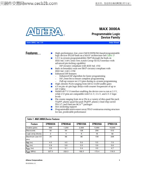
®Altera Corporation 1MAX 3000AProgrammable Logic Device FamilyJune 2002, ver. 3.0Data Sheet DS-M3000A-3.0Features...■High–performance, low–cost CMOS EEPROM–based programmable logic devices (PLDs) built on a MAX ® architecture (see Table 1)■3.3-V in-system programmability (ISP) through the built–in IEEE Std. 1149.1 Joint Test Action Group (JTAG) interface with advanced pin-locking capability –ISP circuitry compliant with IEEE Std. 1532■Built–in boundary-scan test (BST) circuitry compliant with IEEE Std. 1149.1-1990■Enhanced ISP features:–Enhanced ISP algorithm for faster programming –ISP_Done bit to ensure complete programming –Pull-up resistor on I/O pins during in–system programming ■High–density PLDs ranging from 600 to 10,000 usable gates ■4.5–ns pin–to–pin logic delays with counter frequencies of up to 227.3MHz ■MultiVolt TM I/O interface enabling the device core to run at 3.3 V, while I/O pins are compatible with 5.0–V, 3.3–V, and 2.5–V logic levels ■Pin counts ranging from 44 to 256 in a variety of thin quad flat pack (TQFP), plastic quad flat pack (PQFP), plastic J–lead chip carrier (PLCC), and FineLine BGA TM packages ■Hot–socketing support ■Programmable interconnect array (PIA) continuous routing structurefor fast, predictable performance Table 1.MAX3000A Device Features FeatureEPM3032A EPM3064A EPM3128A EPM3256A EPM3512A Usable gates6001,2502,5005,00010,000Macrocells3264128256512Logic array blocks2481632Maximum user I/Opins346696158208t PD (ns)4.5 4.55.0 5.57.5t SU (ns)2.9 2.83.3 3.9 5.6t CO1 (ns)3.0 3.1 3.4 3.54.7f CNT (MHz)227.3222.2192.3172.4116.3捷多邦,您值得信赖的PCB打样专家!MAX 3000A Programmable Logic Device Family Data Sheet...and More Features ■PCI compatible■Bus–friendly architecture including programmable slew–rate control ■Open–drain output option■Programmable macrocell flipflops with individual clear, preset, clock, and clock enable controls■Programmable power–saving mode for a power reduction of over 50% in each macrocell■Configurable expander product–term distribution, allowing up to32 product terms per macrocell■Programmable security bit for protection of proprietary designs■Enhanced architectural features, including:– 6 or 10 pin– or logic–driven output enable signals–Two global clock signals with optional inversion–Enhanced interconnect resources for improved routability–Programmable output slew–rate control■Software design support and automatic place–and–route provided by Altera’s development systems for Windows–based PCs and Sun SPARCstations, and HP 9000 Series 700/800 workstations■Additional design entry and simulation support provided by EDIF2 0 0 and3 0 0 netlist files, library of parameterized modules (LPM),Verilog HDL, VHDL, and other interfaces to popular EDA tools from third–party manufacturers such as Cadence, Exemplar Logic, Mentor Graphics, OrCAD, Synopsys, Synplicity, and VeriBest■Programming support with the Altera master programming unit (MPU), MasterBlaster TM communications cable, ByteBlasterMV TMparallel port download cable, BitBlaster TM serial download cable as well as programming hardware from third–party manufacturers and any in–circuit tester that supports Jam TM Standard Test andProgramming Language (STAPL) Files (.jam), Jam STAPL Byte-Code Files (.jbc), or Serial Vector Format Files (.svf)General Description MAX3000A devices are low–cost, high–performance devices based on the Altera MAX architecture. Fabricated with advanced CMOS technology, the EEPROM–based MAX3000A devices operate with a 3.3-V supply voltage and provide 600 to 10,000 usable gates, ISP, pin-to-pin delays as fast as 4.5 ns, and counter speeds of up to 227.3MHz. MAX3000A devices in the –4, –5, –6, –7, and –10 speed grades are compatible with the timing requirements of the PCI Special Interest Group (PCI SIG) PCI Local Bus Specification, Revision2.2. See Table2.2Altera CorporationAltera Corporation 3MAX 3000A Programmable Logic Device Family Data Sheet The MAX 3000A architecture supports 100% transistor-to-transistor logic (TTL) emulation and high–density small-scale integration (SSI), medium-scale integration (MSI), and large-scale integration (LSI) logic functions. The MAX 3000A architecture easily integrates multiple devices ranging from PALs, GALs, and 22V10s to MACH and pLSI devices. MAX 3000A devices are available in a wide range of packages, including PLCC, PQFP, and TQFP packages. See Table 3.Note:(1)When the IEEE Std. 1149.1 (JTAG) interface is used for in–system programming or boundary–scan testing, four I/O pins become JTAG pins.MAX 3000A devices use CMOS EEPROM cells to implement logic functions. The user–configurable MAX 3000A architecture accommodates a variety of independent combinatorial and sequential logic functions. The devices can be reprogrammed for quick and efficient iterations during design development and debugging cycles, and can be programmed and erased up to 100 times.Table 2.MAX 3000A Speed Grades Device Speed Grade –4–5–6–7–10EPM3032A v v v EPM3064A vv v EPM3128A v v v EPM3256A v v EPM3512A v v Table 3.MAX 3000A Maximum User I/O Pins Note (1)Device 44–Pin PLCC 44–Pin TQFP 100–Pin TQFP 144–Pin TQFP 208–Pin PQFP 256-Pin FineLine BGA EPM3032A 3434EPM3064A 343466EPM3128A 8096EPM3256A 116158EPM3512A 172208MAX 3000A Programmable Logic Device Family Data SheetMAX3000A devices contain 32 to 512 macrocells, combined into groupsof 16 macrocells called logic array blocks (LABs). Each macrocell has aprogrammable–AND/fixed–OR array and a configurable register withindependently programmable clock, clock enable, clear, and presetfunctions. To build complex logic functions, each macrocell can besupplemented with shareable expander and high–speed parallelexpander product terms to provide up to 32 product terms per macrocell.MAX3000A devices provide programmable speed/power optimization.Speed–critical portions of a design can run at high speed/full power,while the remaining portions run at reduced speed/low power. Thisspeed/power optimization feature enables the designer to configure oneor more macrocells to operate at 50% or lower power while adding only anominal timing delay. MAX3000A devices also provide an option thatreduces the slew rate of the output buffers, minimizing noise transientswhen non–speed–critical signals are switching. The output drivers of allMAX3000A devices can be set for 2.5V or 3.3V, and all input pins are2.5–V,3.3–V, and 5.0-V tolerant, allowing MAX3000A devices to be usedin mixed–voltage systems.MAX3000A devices are supported by Altera development systems,which are integrated packages that offer schematic, text—includingVHDL, Verilog HDL, and the Altera Hardware Description Language(AHDL)—and waveform design entry, compilation and logic synthesis,simulation and timing analysis, and device programming. The softwareprovides EDIF 2 0 0 and 3 0 0, LPM, VHDL, Verilog HDL, and otherinterfaces for additional design entry and simulation support from otherindustry–standard PC– and UNIX–workstation–based EDA tools. Thesoftware runs on Windows–based PCs, as well as Sun SPARCstation, andHP 9000 Series 700/800 workstations.f For more information on development tools, see the MAX+PLUS IIProgrammable Logic Development System & Software Data Sheet andtheQuartus Programmable Logic Development System & Software Data Sheet.Functional Description The MAX3000A architecture includes the following elements:■Logic array blocks (LABs)■Macrocells■Expander product terms (shareable and parallel)■Programmable interconnect array (PIA)■I/O control blocksThe MAX3000A architecture includes four dedicated inputs that can be used as general–purpose inputs or as high–speed, global control signals (clock, clear, and two output enable signals) for each macrocell and I/O pin. Figure1 shows the architecture of MAX3000A devices.4Altera CorporationMAX 3000A Programmable Logic Device Family Data Sheet Figure 1. MAX3000A Device Block DiagramNote:(1)EPM3032A, EPM3064A, EPM3128A, and EPM3256A devices have six output enables. EPM3512A devices have10output enables.Logic Array BlocksThe MAX3000A device architecture is based on the linking ofhigh–performance LABs. LABs consist of 16–macrocell arrays, as shownin Figure1. Multiple LABs are linked together via the PIA, a global busthat is fed by all dedicated input pins, I/O pins, and macrocells.Each LAB is fed by the following signals:■36 signals from the PIA that are used for general logic inputs■Global controls that are used for secondary register functionsAltera Corporation 5MAX 3000A Programmable Logic Device Family Data SheetMacrocellsMAX3000A macrocells can be individually configured for eithersequential or combinatorial logic operation. Macrocells consist of threefunctional blocks: logic array, product–term select matrix, andprogrammable register. Figure2 shows a MAX3000A macrocell.Figure 2. MAX3000A MacrocellQCLRNTo PIACombinatorial logic is implemented in the logic array, which providesfive product terms per macrocell. The product–term select matrixallocates these product terms for use as either primary logic inputs (to theOR and XOR gates) to implement combinatorial functions, or as secondaryinputs to the macrocell’s register preset, clock, and clock enable controlfunctions.Two kinds of expander product terms (“expanders”) are available tosupplement macrocell logic resources:■Shareable expanders, which are inverted product terms that are fedback into the logic array■Parallel expanders, which are product terms borrowed from adjacentmacrocellsThe Altera development system automatically optimizes product–termallocation according to the logic requirements of the design.6Altera CorporationMAX 3000A Programmable Logic Device Family Data SheetFor registered functions, each macrocell flipflop can be individuallyprogrammed to implement D, T, JK, or SR operation with programmableclock control. The flipflop can be bypassed for combinatorial operation.During design entry, the designer specifies the desired flipflop type; theAltera development system software then selects the most efficientflipflop operation for each registered function to optimize resourceutilization.Each programmable register can be clocked in three different modes:■Global clock signal mode, which achieves the fastest clock–to–outputperformance.■Global clock signal enabled by an active–high clock enable. A clockenable is generated by a product term. This mode provides an enableon each flipflop while still achieving the fast clock–to–outputperformance of the global clock.■Array clock implemented with a product term. In this mode, theflipflop can be clocked by signals from buried macrocells or I/O pins.Two global clock signals are available in MAX3000A devices. As shownin Figure1, these global clock signals can be the true or the complement ofeither of the two global clock pins, GCLK1 or GCLK2.Each register also supports asynchronous preset and clear functions. Asshown in Figure2, the product–term select matrix allocates product termsto control these operations. Although the product–term–driven presetand clear from the register are active high, active–low control can beobtained by inverting the signal within the logic array. In addition, eachregister clear function can be individually driven by the active–lowdedicated global clear pin (GCLRn).Expander Product TermsAlthough most logic functions can be implemented with the five productterms available in each macrocell, highly complex logic functions requireadditional product terms. Another macrocell can be used to supply therequired logic resources. However, the MAX3000A architecture alsooffers both shareable and parallel expander product terms (“expanders”)that provide additional product terms directly to any macrocell in thesame LAB. These expanders help ensure that logic is synthesized with thefewest possible logic resources to obtain the fastest possible speed. Altera Corporation 78Altera Corporation MAX 3000A Programmable Logic Device Family Data SheetShareable Expanders Each LAB has 16 shareable expanders that can be viewed as a pool of uncommitted single product terms (one from each macrocell) with inverted outputs that feed back into the logic array. Each shareable expander can be used and shared by any or all macrocells in the LAB to build complex logic functions. Shareable expanders incur a small delay (t SEXP ). Figure 3 shows how shareable expanders can feed multiple macrocells.Figure 3. MAX 3000A Shareable Expanders Shareable expanders can be shared by any or all macrocells in an LAB.Parallel Expanders Parallel expanders are unused product terms that can be allocated to a neighboring macrocell to implement fast, complex logic functions. Parallel expanders allow up to 20 product terms to directly feed the macrocell OR logic, with five product terms provided by the macrocell and 15 parallel expanders provided by neighboring macrocells in the LAB. MacrocellProduct-Term Logic Product-Term Select Matrix Macrocell Product-Term Logic 36 Signals from PIA 16 Shared ExpandersMAX 3000A Programmable Logic Device Family Data SheetThe Altera development system compiler can automatically allocate up tothree sets of up to five parallel expanders to the macrocells that requireadditional product terms. Each set of five parallel expanders incurs asmall, incremental timing delay (t PEXP). For example, if a macrocellrequires 14product terms, the compiler uses the five dedicated productterms within the macrocell and allocates two sets of parallel expanders;the first set includes five product terms, and the second set includes fourproduct terms, increasing the total delay by 2 ×t PEXP.Two groups of eight macrocells within each LAB (e.g., macrocells 1through 8 and 9through 16) form two chains to lend or borrow parallelexpanders. A macrocell borrows parallel expanders from lower–numbered macrocells. For example, macrocell 8 can borrow parallelexpanders from macrocell 7, from macrocells 7 and 6, or from macrocells7, 6, and 5. Within each group of eight, the lowest–numbered macrocellcan only lend parallel expanders and the highest–numbered macrocell canonly borrow them. Figure4 shows how parallel expanders can beborrowed from a neighboring macrocell.Figure 4. MAX3000A Parallel ExpandersUnused product terms in a macrocell can be allocated to a neighboring macrocell.Altera Corporation 9MAX 3000A Programmable Logic Device Family Data SheetProgrammable Interconnect ArrayLogic is routed between LABs on the PIA. This global bus is aprogrammable path that connects any signal source to any destination onthe device. All MAX3000A dedicated inputs, I/O pins, and macrocelloutputs feed the PIA, which makes the signals available throughout theentire device. Only the signals required by each LAB are actually routedfrom the PIA into the LAB. Figure5 shows how the PIA signals are routedinto the LAB. An EEPROM cell controls one input to a two-input AND gate,which selects a PIA signal to drive into the LAB.Figure 5. MAX3000A PIA RoutingWhile the routing delays of channel–based routing schemes in masked orFPGAs are cumulative, variable, and path–dependent, the MAX3000APIA has a predictable delay. The PIA makes a design’s timingperformance easy to predict.I/O Control BlocksThe I/O control block allows each I/O pin to be individually configuredfor input, output, or bidirectional operation. All I/O pins have a tri–statebuffer that is individually controlled by one of the global output enablesignals or directly connected to ground or V CC. Figure6 shows the I/Ocontrol block for MAX3000A devices. The I/O control block has 6 or10global output enable signals that are driven by the true or complementof two output enable signals, a subset of the I/O pins, or a subset of theI/O macrocells.10Altera CorporationMAX 3000A Programmable Logic Device Family Data Sheet Figure 6. I/O Control Block of MAX3000A DevicesNote:(1)EPM3032A, EPM3064A, EPM3128A, and EPM3256A devices have six output enables. EPM3512A devices have10output enables.When the tri–state buffer control is connected to ground, the output istri-stated (high impedance), and the I/O pin can be used as a dedicatedinput. When the tri–state buffer control is connected to V CC, the output isenabled.The MAX3000A architecture provides dual I/O feedback, in whichmacrocell and pin feedbacks are independent. When an I/O pin isconfigured as an input, the associated macrocell can be used for buriedlogic.Altera Corporation 1112Altera Corporation MAX 3000A Programmable Logic Device Family Data SheetIn–SystemProgramma-bilityMAX 3000A devices can be programmed in–system via an industry–standard four–pin IEEE Std. 1149.1-1990 (JTAG) interface. In-system programmability (ISP) offers quick, efficient iterations during design development and debugging cycles. The MAX 3000A architecture internally generates the high programming voltages required to program its EEPROM cells, allowing in–system programming with only a single 3.3–V power supply. During in–system programming, the I/O pins are tri–stated and weakly pulled–up to eliminate board conflicts. The pull–up value is nominally 50 k Ω.MAX 3000A devices have an enhanced ISP algorithm for faster programming. These devices also offer an ISP_Done bit that ensures safe operation when in–system programming is interrupted. This ISP_Done bit, which is the last bit programmed, prevents all I/O pins from driving until the bit is programmed.ISP simplifies the manufacturing flow by allowing devices to be mounted on a printed circuit board (PCB) with standard pick–and–place equipment before they are programmed. MAX 3000A devices can be programmed by downloading the information via in–circuit testers, embedded processors, the MasterBlaster communications cable, the ByteBlasterMV parallel port download cable, and the BitBlaster serial download cable. Programming the devices after they are placed on the board eliminates lead damage on high–pin–count packages (e.g., QFP packages) due to device handling. MAX 3000A devices can be reprogrammed after a system has already shipped to the field. For example, product upgrades can be performed in the field via software or modem. The Jam STAPL programming and test language can be used to program MAX 3000A devices with in–circuit testers, PCs, or embedded processors.fFor more information on using the Jam STAPL programming and test language, see Application Note 88 (Using the Jam Language for ISP & ICR via an Embedded Processor), Application Note 122 (Using Jam STAPL for ISP & ICR via an Embedded Processor) and AN 111 (Embedded Programming Using the 8051 and Jam Byte-Code).The ISP circuitry in MAX 3000A devices is compliant with the IEEE Std. 1532 specification. The IEEE Std. 1532 is a standard developed to allow concurrent ISP between multiple PLD vendors.Programmingwith ExternalHardwareMAX 3000A devices can be programmed on Windows–based PCs with an Altera Logic Programmer card, MPU, and the appropriate device adapter. The MPU performs continuity checking to ensure adequate electrical contact between the adapter and the device. fFor more information, see the Altera Programming Hardware Data Sheet.Altera Corporation 13MAX 3000A Programmable Logic Device Family Data SheetThe Altera software can use text– or waveform–format test vectors createdwith the Altera Text Editor or Waveform Editor to test the programmeddevice. For added design verification, designers can perform functionaltesting to compare the functional device behavior with the results ofsimulation.Data I/O, BP Microsystems, and other programming hardwaremanufacturers also provide programming support for Altera devices.fFor more information, see Programming Hardware Manufacturers .IEEE Std.1149.1 (JTAG)Boundary–ScanSupport MAX 3000A devices include the JTAG BST circuitry defined by IEEE Std.1149.1–1990. Table 4 describes the JTAG instructions supported by MAX 3000A devices. The pin-out tables found on the Altera web site ( ) or the Altera Digital Library show the location of the JTAG control pins for each device. If the JTAG interface is notrequired, the JTAG pins are available as user I/O pins.The instruction register length of MAX 3000A devices is 10 bits. TheIDCODE and USERCODE register length is 32 bits. Tables 5 and 6 showthe boundary–scan register length and device IDCODE information forMAX 3000A devices.Table 4.MAX 3000A JTAG InstructionsJTAG InstructionDescription SAMPLE/PRELOADAllows a snapshot of signals at the device pins to be captured and examined during normal device operation, and permits an initial data pattern output at the device pins EXTESTAllows the external circuitry and board–level interconnections to be tested by forcing a test pattern at the output pins and capturing test results at the input pins BYPASS Places the 1–bit bypass register between the TDI and TDO pins, which allows the BSTdata to pass synchronously through a selected device to adjacent devices during normaldevice operationIDCODE Selects the IDCODE register and places it between the TDI and TDO pins, allowing theIDCODE to be serially shifted out of TDOUSERCODE Selects the 32–bit USERCODE register and places it between the TDI and TDO pins,allowing the USERCODE value to be shifted out of TDOISP InstructionsThese instructions are used when programming MAX 3000A devices via the JTAG portswith the MasterBlaster, ByteBlasterMV, or BitBlaster cable, or when using a Jam STAPLfile, JBC file, or SVF file via an embedded processor or test equipment14Altera Corporation MAX 3000A Programmable Logic Device Family Data SheetNotes:(1)The most significant bit (MSB) is on the left.(2)The least significant bit (LSB) for all JTAG IDCODEs is 1.fSee Application Note 39 (IEEE 1149.1 (JTAG) Boundary–Scan Testing in Altera Devices) for more information on JTAG BST.Table 5.MAX 3000A Boundary–Scan Register Length Device Boundary–Scan Register Length EPM3032A 96EPM3064A 192EPM3128A 288EPM3256A 480EPM3512A 624Table 6.32–Bit MAX 3000A Device IDCODE Value Note (1)Device IDCODE (32 bits)Version (4 Bits)Part Number (16 Bits) Manufacturer’s Identity (11 Bits) 1 (1 Bit) (2)EPM3032A 00010111 0000 0011 0010000011011101EPM3064A 00010111 0000 0110 0100000011011101EPM3128A 00010111 0001 0010 1000000011011101EPM3256A 00010111 0010 0101 0110000011011101EPM3512A 00010111 0101 0001 0010000011011101MAX 3000A Programmable Logic Device Family Data SheetFigure7 shows the timing information for the JTAG signals.Figure 7. MAX3000A JTAG WaveformsTable7 shows the JTAG timing parameters and values for MAX3000Adevices.Table 7.JTAG Timing Parameters & Values for MAX3000A DevicesSymbol Parameter Min Max Unitt JCP TCK clock period 100nst JCH TCK clock high time 50nst JCL TCK clock low time 50nst JPSU JTAG port setup time 20nst JPH JTAG port hold time 45nst JPCO JTAG port clock to output25nst JPZX JTAG port high impedance to valid output25nst JPXZ JTAG port valid output to high impedance25nst JSSU Capture register setup time20nst JSH Capture register hold time45nst JSCO Update register clock to output25nst JSZX Update register high impedance to valid output25nst JSXZ Update register valid output to high impedance25ns Altera Corporation 15MAX 3000A Programmable Logic Device Family Data SheetProgrammable Speed/Power Control MAX3000A devices offer a power–saving mode that supports low-power operation across user–defined signal paths or the entire device. This feature allows total power dissipation to be reduced by 50% or more because most logic applications require only a small fraction of all gates to operate at maximum frequency.The designer can program each individual macrocell in a MAX3000A device for either high–speed or low–power operation. As a result, speed-critical paths in the design can run at high speed, while the remaining paths can operate at reduced power. Macrocells that run at low power incur a nominal timing delay adder (t LPA) for the t LAD, t LAC, t IC, t ACL, t EN, t CPPW and t SEXP parameters.Output Configuration MAX3000A device outputs can be programmed to meet a variety of system–level requirements.MultiVolt I/O InterfaceThe MAX3000A device architecture supports the MultiVolt I/O interface feature, which allows MAX3000A devices to connect to systems with differing supply voltages. MAX3000A devices in all packages can be set for 2.5–V, 3.3–V, or 5.0–V I/O pin operation. These devices have one set of V CC pins for internal operation and input buffers (VCCINT), and another set for I/O output drivers (VCCIO).The VCCIO pins can be connected to either a 3.3–V or 2.5–V power supply, depending on the output requirements. When the VCCIO pins are connected to a 2.5–V power supply, the output levels are compatible with 2.5–V systems. When the VCCIO pins are connected to a 3.3–V power supply, the output high is at 3.3V and is therefore compatible with 3.3-V or 5.0–V systems. Devices operating with V CCIO levels lower than 3.0V incur a nominally greater timing delay of t OD2 instead of t OD1. Inputs can always be driven by 2.5–V, 3.3–V, or 5.0–V signals.Table8 summarizes the MAX3000A MultiVolt I/O support.Note:(1)When V CCIO is 3.3 V, a MAX 3000A device can drive a 2.5–V device that has 3.3–Vtolerant inputs.Table 8.MAX3000A MultiVolt I/O SupportV CCIO Voltage Input Signal (V)Output Signal (V)2.53.3 5.0 2.5 3.3 5.02.5v v v v3.3v v v v v v16Altera CorporationMAX 3000A Programmable Logic Device Family Data SheetOpen–Drain Output OptionMAX3000A devices provide an optional open–drain (equivalent toopen-collector) output for each I/O pin. This open–drain output enablesthe device to provide system–level control signals (e.g., interrupt andwrite enable signals) that can be asserted by any of several devices. It canalso provide an additional wired–OR plane.Open-drain output pins on MAX3000A devices (with a pull-up resistor tothe 5.0-V supply) can drive 5.0-V CMOS input pins that require a high V IH.When the open-drain pin is active, it will drive low. When the pin isinactive, the resistor will pull up the trace to 5.0V, thereby meeting CMOSrequirements. The open-drain pin will only drive low or tri-state; it willnever drive high. The rise time is dependent on the value of the pull-upresistor and load impedance. The I OL current specification should beconsidered when selecting a pull-up resistorSlew–Rate ControlThe output buffer for each MAX3000A I/O pin has an adjustable outputslew rate that can be configured for low–noise or high–speedperformance. A faster slew rate provides high–speed transitions forhigh-performance systems. However, these fast transitions may introducenoise transients into the system. A slow slew rate reduces system noise,but adds a nominal delay of 4 to 5 ns. When the configuration cell isturned off, the slew rate is set for low–noise performance. Each I/O pinhas an individual EEPROM bit that controls the slew rate, allowingdesigners to specify the slew rate on a pin–by–pin basis. The slew ratecontrol affects both the rising and falling edges of the output signal. Design Security All MAX3000A devices contain a programmable security bit that controlsaccess to the data programmed into the device. When this bit isprogrammed, a design implemented in the device cannot be copied orretrieved. This feature provides a high level of design security becauseprogrammed data within EEPROM cells is invisible. The security bit thatcontrols this function, as well as all other programmed data, is reset onlywhen the device is reprogrammed.Generic Testing MAX3000A devices are fully tested. Complete testing of eachprogrammable EEPROM bit and all internal logic elements ensures 100%programming yield. AC test measurements are taken under conditionsequivalent to those shown in Figure8. Test patterns can be used and thenerased during early stages of the production flow.Altera Corporation 17。