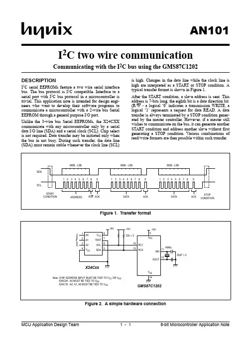
AN101I 2C two wire communicationCommunicating with the I 2C bus using the GMS87C1202DESCRIPTIONI 2C serial EEPROMs feature a two wire serial interface bus. The bus protocol is I 2C compatible. Interface to a serial port with I 2C bus protocol in a microcontroller is trivial. This application note is intended for design engi-neers who want to develop their software programs to communicate a microcontroller with a 2-wire bus Serial EEPROM through a general purpose I/O port.Unlike the 3-wire bus Serial EEPROMs, the X24CXX communicate with any microcontroller only by a serial data I/O line (SDA) and a serial clock (SCL). Chip select is not required. Data transfer may be initiated only when the bus in not busy. During such transfer, the data line (SDA) must remain stable whenever the clock line (SCL)is high. Changes in the data line while the clock line is high are interpreted as a START or STOP condition. A typical transfer format is shown in Figure 1.After the START condition, a slave address is sent. This address is 7-bits long, the eighth bit is a data direction bit.(R/W - a logical ‘0’ indicates a transmission WRITE, a logical ‘1’ represents a request for data READ. A data transfer is always terminated by a STOP condition gener-ated by the master controller. However, if a master still wishes to communicate on the bus, it can generate another START condition and address another slave without first generating a STOP condition. Various combinations of read/write formats are then possible within such transfer.Figure 1. Transfer formatFigure 2. A simple hardware connection189234567189234567189234567ADDRESS R/W ACK ACK ACKDATA DATA STOP CONDITIONSTART CONDITIONSDASCLMSB - LSBMSB - LSB MSB - LSB22k × 2V CC SCL SDAA0A1A2VSSRC1RC01516111214123487655XIN XOUTV DDV SS+5V +5V +5VGMS87C1202X24CxxTEST Note: CHIP ADDRESS INPUT MUST BE TIED TO V CC OR V SS .X24C04 : A0 MUST BE TIED TO V SS .X24C16 : A2, A1, A0 MUST BE TIED TO V SS .4MHz20pF × 2I 2C two wire communicationAn example program has been provided in Appendix A containing all GMS87C1202 routines needed to exercise a X24C02 device. A simple hardware connection is illus-trated in Figure 2. A maximum of eight X24C02, or four X24C04’s can be addressed by a microcontroller on the same two wire bus without additional interfaces. Each device is identified by its Chip Address and will only respond to the correct slave address. A detailed bus flow is shown in Figure 3. Figure 3 as shown below describes how the bit stream is set up for READ and WRITE mode in the microcomputer programming software prior tosending it on the two wire serial bus.The stop condition, after the one byte data write sequence,starts the internal self-timed write cycle which may last up to 0.56 milliseconds (start+150µs per byte). Acknowledge signal should be monitored during this period.....Author:Jongpil ShinMCU application team e-mail: jpshin@Figure 3. Setting the internal word address of the X24CXXFigure 4. Byte Write SequenceFigure 5. Read Mode SequenceSCL11A2A1A0WAckA7A6A4A5A3A2A1A0AckSDA1234567SD1. START CONDITION2. 4 BIT DEVICE CODE 1010 FOR X24C023. DEVICE ADDRESS A0=BANK SELECTOR, HIGH ORDER ADDRESS BIT A8 FOR X24C044. 0=WRITE TO ADDRESS REGISTER5. EEPROM DRIVES BUS LOW WITH ACKNOWLEDGEMENT (TIMEOUT IF NO RESPONSE)6. ADDRESS FOR DATA, A7 - A0 (MSB-LSB)7. BUS LOW FOR ACKNOWLEDGEMENTA2, A1, A0=BANK SELECTOR, HIGH ORDER ADDRESS BIT A10, A9, A8 FOR X24C26SCL1010A2A1A0R Ack D7D6D4D5D3D2D1D0Ack1234567SD1. START CONDITION2. 4 BIT DEVICE CODE 1010 FOR X24CXX3. DEVICE ADDRESS A2, A1, A0. A0=BANK SELECTOR, HIGH ORDER ADDRESS BIT A8 FOR X24C04.4. 1=READ MODE5. ACKNOWLEDGE FROM EEPROM D7~~~~86. FIRST DATA BYTE7. SECOND DATA BYTE, ETC.8 STOP CONDITIONREAD UP TO 256 BYTES (X24C02)READ UP TO 512 BYTES (X24C04)READ UP TO 2K BYTES (X24C16)A2, A1, A0 = BANK SELECTOR, HIGH ORDER ADDRESS BIT A10, A9, A8 FOR X24C16I2C two wire communicationAppendix A:GMS800 series MICOM ASSEMBLER Fri Aug 20 13:14:24 1999(PAGE 1)1 PAGE 100002 ;*******************************************************************************3 ; PROGRAM DESCRIPTION:4 ; Many system are implemented by IIC communication theory, it is came from5 ; Philips and use two wires, one is clock line and another is data line.6 ;-------------------------------------------------------------------------------7 ; MICROCONTROLLER : GMS87C1202 (2K ROM, 20 PIN DIP)8 ; OPER. FREQUENCY : 4MHz9 ; SERIAL EEPROM : X24C02 (2KBIT, 8 PIN DIP)10 ;-------------------------------------------------------------------------------11 ; programmed by Jongpil Shin (HEI) on 1999.08.20 Version 1.0012 ;*******************************************************************************13 ;14 ; TYPICAL APPLICATION CIRCUIT15 ;16 ; +-------------------+17 ; | (__) | +5V18 ; 1|RA4/AN4 AN3/RA3|20 |19 ; | | +---+-----+20 ; 2|RA5/AN5 AN2/RA2|19 | | |21 ; | | | | |22 ; 3|RA6/AN6 G AN1/RA1|18 / /22K |23 ; | M | / / | 7+--------+24 ; 4|RA7/AN7 S EC0/RA0|17 | | +--|VDD WP|--+25 ; | 8 | | | 6| | |26 ; +5V 5|VDD 7 RC1|16-------+--------|SCL A2|--+27 ; | C | | 5| | |28 ; 6|RB0/AN0 1 RC0|15--------+--------|SDA A1|--+29 ; | 2 | | | |30 ; 7|RB1/BUZ 0 VSS|14 GND | A0|--+31 ; | 2 | | | |32 ; 8|RB2/INT0 /RESET|13 /Reset | VSS|--+33 ; | | +--------+ |34 ; 9|RB3/INT1 XOUT|12 X-tal Out 24C02 GND35 ; | | EEPROM36 ; 10|RB4/PWM/COMP XIN|11 X-tal In37 ; | |38 ; +-------------------+39 ; GMS87C120240 ;41 ;*****************************************************************42 ; * Included Subroutines43 ; IIC_Rx : Receive one byte through the IIC bus44 ; IIC_Tx : Transmmit one byte through the IIC bus45 ; IIC_start : Goes to "start condition"46 ; IIC_stop : Goes to "stop condition"47 ;*****************************************************************48 ; * Using I/O pins49 ; PIO_SDA : IIC bus serial data line port, the RC0 pin is used50 ; PO_SCL : IIC bus serial clock line port, the RC1 pin is used51 ;*****************************************************************52 ; * Used RAM53 ; - none54 ;*****************************************************************55 ;56 RC EQU 0C4H57 RCIO EQU 0C5H58I2C two wire communication59 INPUT_MODE EQU 0000_0010B ; make SDA pin as an input port to read acknowledge60 OUTPUT_MODE EQU 0000_0011B ; make SDA pin as an output port to write bit and acknowledge61 PO_SCL EQU 1,RC62 PIO_SDA EQU 0,RC6364 ;************** VECTOR AREA *****************65 ;66 ORG 0FFFEH67 FFFE 00F8 DW RESET ;Reset Vector6869 ORG 0F800H7071 F800 1E7F RESET: LDX #07FH ;Initialize SP = #7FH72 F802 8E TXSP73 F803 E403C4 LDM RC,#0000_0011B74 F806 E403C5 LDM RCIO,#0000_0011B75 F809 1BCBF8 JMP START7677 ;*******************************************************************************78 ; Write one byte data into the EEPROM79 ; - Write one byte data (Accumulator) at address X of EEPROM80 ;*******************************************************************************81 ; Input parameter82 ; - Accumulator : write data83 ; - X register : write address84 ; Output parameter85 ; - None86 ; Scrached data87 ; - Y register : shift bit counter88 ;-------------------------------------------------------------------------------89 ; Thie write cycle time is the time(max10ms) from a valid stop condition of a90 ; write sequence to the end of the internal erase/program cycle, During the write91 ; cycle, the EEPROM bus interface circuits are disabled, SDA is allowed to92 ; remain high, and the device dows not respond to its slave address.93 ;*******************************************************************************9495 write_byte:96 F80C 0E PUSH A97 F80D 3B96F8 CALL IIC_start98 F810 C4A0 LDA #0A0H ; set to be "byte write condition"99 F812 3B3DF8 CALL IIC_Tx ; tx. one byte via IIC bus100 F815 EE XAX ; set word address (X -> A)101 F816 3B3DF8 CALL IIC_Tx ; tx. one byte(address) to slave102 F819 0D POP A ; set one byte data to be wrote103 F81A 3B3DF8 CALL IIC_Tx ; tx. one byte(data) to slave104 F81D 3BA7F8 CALL IIC_stop ; make "stop condition"105 F820 6F RET106 ;107 ;*******************************************************************************108 ; Read one byte data from the EEPROM109 ; - One byte data is read from EEPROM address X of EEPROM110 ;*******************************************************************************111 ; Input parameter112 ; - X register : read address113 ; Output parameter114 ; - Accumulator : one byte data115 ; Scrached data116 ; - Y register : shift bit counter117 ;*******************************************************************************118 ReadFromEEPROM:119 read_byte:120 F821 3B96F8 CALL IIC_startI2C two wire communication 121 F824 C4A0 LDA #0A0H ; set to be "byte write condition"122 F826 3B3DF8 CALL IIC_Tx ; transmit one byte (slave address) via IIC bus123 F829 EE XAX ; set word address (X -> A)124 F82A 3B3DF8 CALL IIC_Tx ; transmit one byte(word address) to slave125 F82D 3B96F8 CALL IIC_start ; set to be start condition126 F830 C4A1 LDA #0A1H ; set to be "byte write condition"127 F832 3B3DF8 CALL IIC_Tx ; transmit one byte (slave address) via IIC bus128 F835 FF NOP129 F836 3B7BF8 CALL IIC_Rx ; receive one byte(data) to slave130 F839 3BA7F8 CALL IIC_stop ; make "stop condition"131 F83C 6F RET132 ;133 ;----------------------------------------------------------134 ; TRANSMIT ONE BYTE DATA VIA IIC BUS135 ;----------------------------------------------------------136 ; Entry : Accumulator (to be wrote transmit data)137 ; Output : Carry (0=ok, 1=No ack, maybe error)138 ; Scratch data : Y register is used shift counter and will be decremented139 ;----------------------------------------------------------140 F83D E403C5 IIC_Tx: LDM RCIO,#OUTPUT_MODE ; set SDA as an output mode141142 F840 3E06 LDY #6 ; prepare shift counter seven clock counter143 iic_loop: ; Transmit seven clocks144 F842 28 ROL A ; get one bit to be send145 F843 EBC410 STC PIO_SDA ; transmit one bit through the data line146 F846 FF NOP147 F847 FF NOP148 F848 FF NOP149 F849 21C4 SET1 PO_SCL ; make clock rising edge150 F84B FF NOP151 F84C FF NOP152 F84D 31C4 CLR1 PO_SCL ; make clock falling edge153 F84F BE DEC Y ; eight bits done ?154 F850 10F0 BPL iic_loop ; no -> coutinue tx. the bit155 ; Transmit eighth clock156 ; - Ack. form slave is output when eighth clock is fall, so SDA pin have to be input mode157 ; as below158 F852 FF NOP159 F853 28 ROL A160 F854 EBC410 STC PIO_SDA161 F857 5009 BCC iic_l3 ; LSB is 0 ?162 F859 21C4 SET1 PO_SCL ; No, LSB is "1", SDA have to be input mode before fall...163 F85B E402C5 LDM RCIO,#INPUT_MODE ; ... of eighth clock to prevent skew with Ack. from slave 164 F85E 31C4 CLR1 PO_SCL165 F860 2F0C BRA check_ack166 F862 21C4 iic_l3: SET1 PO_SCL ; Yes, LSB is "0", there is no ban skew condition between SDA and Ack.167 F864 FF NOP ; SDA goes to be input mode normally after fall of eighth clock 168 F865 FF NOP169 F866 FF NOP170 F867 FF NOP171 F868 FF NOP172 F869 31C4 CLR1 PO_SCL173 F86B E402C5 LDM RCIO,#INPUT_MODE ; make SDA port as an input port to read ack. signal174 ; all eight bits data is transmitted,175 ; this time acknowledge bit have to be checked176 check_ack: ; Transmit ninth clock177 F86E 3BBEF8 CALL delay1178 F871 21C4 SET1 PO_SCL ; Ninth clock cycle output to read Ack.179 F873 CBC410 LDCB PIO_SDA ; Read Ack. If Carry is 1, then error180 F876 31C4 CLR1 PO_SCL ; for next procedure181 F878 01C4 SET1 PIO_SDA ; make to be initial state...I2C two wire communication182 F87A 6F RET183 ;----------------------------------------------------------184 ; RECEIVE ONE BYTE DATA VIA IIC BUS185 ;----------------------------------------------------------186 ; Entry : None187 ; Output : Accumulator (Received one byte data)188 ; Scratch data : Y will be decremented189 ;----------------------------------------------------------190 F87B 3E07 IIC_Rx: LDY #7 ; prepare shift counter191 F87D FF iic_l2: NOP192 F87E FF NOP193 F87F 21C4 SET1 PO_SCL ; request to slave (EEPROM) output one bit194 F881 CBC400 LDC PIO_SDA ; Read one bit and store to Carry195 F884 28 ROL A196 F885 31C4 CLR1 PO_SCL ; end read one bit197 F887 BE DEC Y ; all eight bits done ?198 F888 10F3 BPL iic_l2 ; no -> read rx. data coutinuously199 ;200 ; It should be noted that the ninth clock cycle of the read operation is not a "don't care". 201 ; To terminate a read operation, the master must either issue a stop condition during the 202 ; ninth cycle or hold SDA HIGH during the ninth clock cycle and then issue a stop condition. 203 F88A E403C5 LDM RCIO,#OUTPUT_MODE ; make SDA port as an input port to read ack. signal 204 F88D 01C4 SET1 PIO_SDA ; hold SDA is "high" during ninth clock205 F88F FF NOP206 F890 21C4 SET1 PO_SCL ; generate ninth clock207 F892 FF NOP ; delay208 F893 31C4 CLR1 PO_SCL ; end session209 F895 6F RET210 ;----------------------------------------------------------211 ; Make EEPROM to be "START CONDITION"212 ; - All commands are preceded by the start condition which213 ; is a HIGH to LOW transition of SDA when SCL is HIGH.214 ;----------------------------------------------------------215 IIC_start:216 F896 E403C5 LDM RCIO,#OUTPUT_MODE ; set SDA as an output mode217 F899 01C4 SET1 PIO_SDA ; initialize SDA to be normal state218 F89B 21C4 SET1 PO_SCL ; initialize SDA to be normal state219 F89D 3BB5F8 CALL delay4220 F8A0 11C4 CLR1 PIO_SDA ; make start condition throught execution below line221 F8A2 FF NOP222 F8A3 FF NOP223 F8A4 31C4 CLR1 PO_SCL224 F8A6 6F RET225 ;----------------------------------------------------------226 ; Make EEPROM to be "STOP CONDITION"227 ; - All communication must be terminated by a sotp condition,228 ; which is a LOW to High transition of SDA when SCL is HIGH.229 ;----------------------------------------------------------230 F8A7 E403C5 IIC_stop: LDM RCIO,#OUTPUT_MODE ; set SDA as an output mode231 F8AA 11C4 CLR1 PIO_SDA232 F8AC FF NOP233 F8AD FF NOP234 F8AE 21C4 SET1 PO_SCL235 F8B0 FF NOP236 F8B1 FF NOP237 F8B2 01C4 SET1 PIO_SDA238 F8B4 6F RET239240 ;----------------------------------------------------------241 ; Delay routine242 ; - delay1 : 13 cycles long, 13*0.5us = 6.5us243 ; - delay2 : 26 cycles long, 26*0.5us = 13.0usI2C two wire communication 244 ; - delay4 : 52 cycles long, 52*0.5us = 26.0us245 ; - delay4 : 104 cycles long, 104*0.5us = 52.0us246 ;----------------------------------------------------------247248 F8B5 3BB8F8 delay4: call delay3249 F8B8 3BBBF8 delay3: call delay2250 F8BB 3BBEF8 delay2: call delay1251 F8BE 6F delay1: RET ; execution time needs 5 cycle252253 delay10ms: ; approxmately 10ms254 F8BF 1E0E LDX #14255 F8C1 3EED dx1: LDY #0EDH256 F8C3 BE dy1: DEC Y257 F8C4 70FD BNE dy1258 F8C6 AF DEC X259 F8C7 70F8 BNE dx1260 F8C9 FF NOP261 F8CA 6F RET262263 ;Test program to read and wirite random264 F8CB 1E03 START: LDX #3 ; set r/w loc. = 2265 F8CD C455 LDA #85 ; write 85266 F8CF 3B0CF8 CALL write_byte ; write 85 to EEPROM267 F8D2 3BBFF8 CALL delay10ms ; delay 10ms for write processing268 F8D5 1E03 LDX #3269 F8D7 3B21F8 CALL read_byte270 F8DA 4455 CMP #85271 F8DC F003 BEQ CORRECT272 WRONG:273 F8DE 1BDEF8 JMP WRONG274 CORRECT:275 F8E1 1BE1F8 JMP CORRECT276277 END-- 0 Error(s) ----- Total Machine Code : 230 Bytes --。