SiC肖特基二极管电热宏模型
- 格式:pdf
- 大小:222.58 KB
- 文档页数:4
600V碳化硅结势垒肖特基二极管电学应力下的退化机理及模型研究中期报告本研究旨在探究600V碳化硅结势垒肖特基二极管在电学应力下的退化机理及建立相应的模型。
本次报告主要介绍研究背景、研究目的、研究进展等方面的内容。
一、研究背景随着电力电子设备的快速发展,高压、大功率、高温等极端环境下的电子元器件的需求越来越大,传统的硅基元器件已经不能满足这些需求。
为了提高功率密度、降低失效率和延长寿命,无碳化硅(SiC)的宽禁带半导体材料成为当今制造高功率、高性能电子元器件的热门材料之一。
然而,高压、高功率下碳化硅肖特基二极管的失效机理和退化行为仍然没有完全研究清楚,这也成为限制碳化硅应用范围的主要因素之一。
因此,本文旨在研究肖特基二极管在电学应力下的退化机理,建立退化模型,以便更好地实现碳化硅肖特基二极管的应用。
二、研究目的本研究的主要目的是:1)探究碳化硅肖特基二极管在电学应力下的退化规律及机理;2)建立碳化硅肖特基二极管的失效模型,预测其寿命;3)通过实验数据验证模型的准确性和可靠性。
三、研究进展目前,已完成了以下工作:1)收集了大量与碳化硅肖特基二极管失效机理相关的文献,并进行了仔细的阅读和分析;2)搭建了实验平台,开始进行退化实验;3)本文提出了一种新型的肖特基二极管失效模型,通过对建模过程的分析和优化,提高了模型的预测准确性;4)对实验数据进行了初步分析,初步验证了所建模型的准确性。
四、展望未来的研究将集中于以下几个方面:1)继续进行实验,收集更多的退化数据,以验证和改善退化模型;2)在建立模型的基础上,探索进一步提高碳化硅肖特基二极管性能和寿命的方法;3)将所建模型应用于碳化硅肖特基二极管的实际应用中,以提高碳化硅肖特基二极管更广泛的应用价值。
4H-SiC肖特基二极管γ射线探测器的模型与分析张林;张义门;张玉明;张书霞;汤晓燕;王悦湖【期刊名称】《强激光与粒子束》【年(卷),期】2008(020)005【摘要】在研究反偏压4H-SiC肖特基二极管作为γ射线探测器工作机理的基础上建立了数值模型,模拟了不同偏压和辐照剂量率下探测器的暗电流、工作电流和灵敏度.模拟结果表明:探测器的灵敏度随反向偏压的增加而上升;对于Au/SiC肖特基二极管,有源区掺杂数密度为2.2×1015 cm-3时,0 V偏压下探测器的灵敏度为13.9×10⁻⁹ C/Gy,100 V偏压下为24.5×10⁻⁹ C/Gy.计算结果与实验数据符合得较好.【总页数】5页(P854-858)【作者】张林;张义门;张玉明;张书霞;汤晓燕;王悦湖【作者单位】西安电子科技大学,微电子学院,教育部宽禁带半导体材料重点实验室,西安,710071;西安电子科技大学,微电子学院,教育部宽禁带半导体材料重点实验室,西安,710071;西安电子科技大学,微电子学院,教育部宽禁带半导体材料重点实验室,西安,710071;西安武警工程学院,通信系,西安,710086;西安电子科技大学,微电子学院,教育部宽禁带半导体材料重点实验室,西安,710071;西安电子科技大学,微电子学院,教育部宽禁带半导体材料重点实验室,西安,710071【正文语种】中文【中图分类】O472;TL816【相关文献】1.4H-SiC肖特基二极管温度传感器模型分析 [J], 申君君;王巍;王玉青2.4H-SiC肖特基势垒二极管伏-安特性的解析模型 [J], 常远程;张义门;张玉明3.4H-SiC肖特基二极管α探测器研究 [J], 陈雨;范晓强;蒋勇;吴健;白立新;柏松;陈刚;李理4.基于4H-SiC肖特基二极管的中子探测器 [J], 蒋勇;吴健;韦建军;范晓强;陈雨;荣茹;邹德慧;李勐;柏松5.基于4H-SiC肖特基势垒二极管的γ射线探测器 [J], 杜园园;张春雷;曹学蕾因版权原因,仅展示原文概要,查看原文内容请购买。
碳化硅(SiC)肖特基二极管
H.卡普斯;M.科拉奇;C.米斯尼尔;R.卢普;L.兹弗里夫;J.M.汉克柯
【期刊名称】《电力电子》
【年(卷),期】2003(000)0Z1
【摘要】崭新的碳化硅(SiC)肖特基二极管优于它的竞争者,具有600V的阻断电压;而且没有反向恢复电荷和反向恢复电流。
【总页数】4页(P)
【作者】H.卡普斯;M.科拉奇;C.米斯尼尔;R.卢普;L.兹弗里夫;J.M.汉克柯
【作者单位】
【正文语种】中文
【中图分类】TN311.7
【相关文献】
1.SiC(碳化硅)肖特基二极管提高升压型交换器性能 [J], 刘鹿生
2.低损耗碳化硅(SiC)肖特基势垒二极管 [J],
3.快速恢复外延二极管和SiC肖特基二极管 [J], 魏明宇
4.Littelfuse碳化硅(SiC)肖特基二极管降低能源成本和空间要求 [J],
5.600 V-30 A 4H-SiC肖特基二极管作为IGBT续流二极管的研究 [J], 李宇柱;倪炜江;李哲洋;李赟;陈辰;陈效建
因版权原因,仅展示原文概要,查看原文内容请购买。
新型4H-SiC肖特基二极管的仿真与分析李俊楠;战可涛【摘要】A novel structure for a 4H-SiC Schottky barrier diode (SBD) with an inclined plane and field rings has been proposed. The silvaco computer aided design (TCAD) software, which is based on semiconductor theory, has been used to simulate the structures of the new 4H-SiC SBD and a 4H-SiC SBD with the conventional structure and the electric V-I characteristics, the breakdown voltage and heat distribution of the 4H-SiC SBD devices with different structures were compared. The new 4H-SiC SBD had a significantly better performance in terms of electric V-I characteristics and heat distribution in devices, and had a breakdown voltage of 2300 V.%设计了斜面结构碳化硅肖特基二极管(4H-SiC SBD)并且在器件中加入场环结构,通过基于半导体物理理论的计算机辅助设计软件( Silvaco-TCAD)分析计算了常规结构和新结构SiC -SBD器件的V-I特性、击穿电压、温度热学分布.对比计算结果,可知新结构SiC-SBD器件击穿电压提高至2300V,导通电阻减小,温度热学分布明显优于常规结构SiC-SBD器件.【期刊名称】《北京化工大学学报(自然科学版)》【年(卷),期】2012(039)004【总页数】5页(P117-121)【关键词】4H-SiC;肖特基二极管;击穿电压;V-I特性【作者】李俊楠;战可涛【作者单位】北京化工大学理学院,北京100029;北京化工大学理学院,北京100029【正文语种】中文【中图分类】TN386随着电力电子和智能电网行业的发展,对大功率半导体器件的性能指标要求越来越高。

高压4H-SiC结势垒肖特基二极管的研究的开题报告题目:高压4H-SiC结势垒肖特基二极管的研究一、研究背景随着电力系统的发展和智能化程度的提高,对于高压、高温、高频、高性能功率电子器件的需求日益增加。
当前,SiC半导体材料作为一种新型的宽禁带半导体材料,因其高击穿电压、高热传导性能、高频能力以及高温性能等优良特性,被认为是代替传统硅材料的最有潜力的材料之一。
肖特基二极管(SBD)作为一种基础功率电子器件,具有反压小、开关速度快、漏电流小等优点,广泛应用于高压、高温、高速、高频等领域。
而基于SiC材料的肖特基二极管,由于SiC的优异特性,更能满足高性能功率器件的需求。
因此,研究SiC 材料的势垒肖特基二极管,对于SiC材料的开发和应用具有重要意义。
二、研究目的本次研究旨在研究高压4H-SiC结势垒肖特基二极管的特性和优化制备工艺,以实现性能的最大化。
具体任务包括:1.探究4H-SiC材料的物理、化学特性以及制备方法。
2.设计高压4H-SiC结势垒肖特基二极管的器件结构。
3.通过模拟计算,研究该器件的电学特性。
4.利用制备工艺优化方法,制备出高品质的器件。
5.分析实验结果,评估该器件的性能并探究其优化方法。
三、研究内容1. 4H-SiC材料的物理、化学特性和制备方法研究该部分主要包括对4H-SiC材料的物理、化学特性进行探究和分析,包括材料的微观结构、禁带宽度、载流子迁移率等,以及关联的制备方法。
2. 高压4H-SiC结势垒肖特基二极管器件结构设计该部分主要包括对高压4H-SiC结势垒肖特基二极管器件结构的设计和优化。
其中包括根据不同应用场景的要求,确定器件的尺寸和结构设计,包括肖特基结的尺寸、阳极结的尺寸等。
3. 电学特性的模拟计算该部分主要包括对高压4H-SiC结势垒肖特基二极管的电学特性进行模拟计算。
在软件仿真平台上进行电学仿真,得出器件的电学性能,包括开启电压、正向电阻、反向漏电流等。
4. 器件制备该部分主要包括制备高质量的高压4H-SiC结势垒肖特基二极管器件的制备工艺研究。
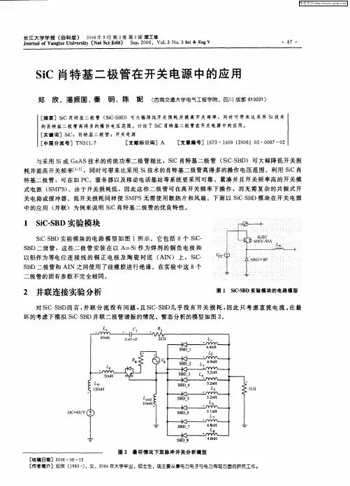
4H—SiC肖特基二极管载流子输运的温度效应作者:童武林孙玉俊刘益宏赵高杰陈之战来源:《上海师范大学学报·自然科学版》2015年第04期摘要:以Cree公司生产的碳化硅肖特基二极管为研究对象,对其进行IV测试.通过对实验数据的理论模拟,研究了碳化硅肖特基二极管的载流子输运机理及温度效应.研究结果表明:温度升高,碳化硅肖特基二极管的肖特基势垒高度降低,漏电流急剧增加.正向导通时符合热电子发射机理,镜像力和隧穿效应共同作用使得反向偏压下的漏电流增加并能较好地和实验值相一致.关键词:碳化肖特基二极管;热电子发射;镜像力;隧穿效应;温度中图分类号: TN 303 文献标志码: A 文章编号: 10005137(2015)040430050 引言碳化硅(SiC)材料的宽禁带、高热导率、高饱和电子漂移速度、高击穿电场等特性决定了其在高温、大功率领域的巨大应用潜力,对国民经济和国防建设将起到重要的推动作用.SiC 存在很多多型结构,其中最常见的是具有立方闪锌矿结构的3CSiC(又称(β-SiC)和六方纤锌矿结构的4HSiC和6HSiC(又称α-SiC)[1].4HSiC耐受温度高达1580 K,器件具有优良的高温工作特性,减少或去除设备中的冷却散热系统,使系统小型化.目前,美国、欧盟、日本等发达国家正竞相投入巨资对SiC材料和器件进行研究.在SiC功率器件中,肖特基二极管(SBD)因其优异的性能而备受关注.美国国防部从20世纪90年代就开始支持SiC功率器件的研究,1992年就研制出阻断电压为400 V的SiC SBD.SiC SBD于21世纪初成为首例市场化的SiC电力电子器件.由于SBD在导通过程中没有额外载流子的注入和储存,因而反向恢复电流小、关断过程很快、开关损耗小.由于所有金属与硅(Si)的功函数差都不很大,因此传统的Si SBD的肖特基势垒较低,反向漏电流偏大,阻断电压较低,只能用于一二百伏的低电压场合,且工作温度不能超过423 K.SiC SBD弥补了Si基SBD的不足,许多金属(如镍、金、钯、钛、钴、钼等)都可以与SiC形成势垒高度超过1 eV的肖特基接触[2-3],因此是高压快速与低功率损耗、耐高温相结合的理想器件.由于器件本身在工作时会产生热量,导致器件的温度变化,温度对器件中载流子的运动与分布会产生影响,从而影响器件的性能,因此对于SiC SBD的输运机理及温度效应的研究十分必要[4].1 实验本实验研究所用器件是Cree公司出售的SiC SBD,产品型号为C3D08065I,基本参数如下:反向重复峰值电压为650 V,398 K下的连续正向电流为8 A,室温下的最大耗散功率约为48 W[5].采用4200SCS半导体参数分析仪,通过引脚测量SiC SBD的IV曲线,测量电压范围为-200~1 V(反向200 V为最大量程),测量温度为300、350、400、450 K(其中反向测量到500 K).通过查阅相关文献资料,获得SiC SBD的基本参数,根据半导体理论,对测试数据进行拟合分析,研究导通机理及温度效应.2 结果与讨论图1是300、350、400、450 K温度下测试得到的正向IFVF曲线.当所加正向电压较大时,根据二极管的折线模型,该段IV特性曲线可以用线性进行拟合,通过与VF轴的截距可得到正向导通电压.图1插图是正向导通电压与温度的关系,当温度升高时,正向导通电压呈线性下降趋势.由拟合数据可知,温度每升高1K,正向导通电压就降低0.00181 V,300 K时的正向导通电压为0.80 V,450 K时的正向导通电压下降到0.53V.通过温度对导通电压的影响关系曲线有利于设置正常的工作电压范围.必须指出的是,通过上述方法提取理想因子n和肖特基势垒高度ns有一个优点,即它与肖特基有效电学接触面积无关.根据图1测试的IF-VF数据,做出不同温度下的ln JF-VF曲线,利用公式(3)和(4),可求出不同温度下的理想因子n和势垒高度ns,它们随温度的变化规律如图2所示.在室温时,n最小为1.12,350 K时n达到最大为1.19,400 K和450 K时的n值为1.16和1.17.在测量温度范围内,SBD的理想因子都大于1,但温度的变化对n值影响不大,说明正向导通时以热电子发射机理为主.随着温度升高,载流子浓度升高,肖特基势垒高度明显降低,从室温下的1.26 eV降低到450 K时的0.89 eV.外加反向电压时,当测试温度在300、350和400 K时,漏电流很小,小于测试系统的分辨极限,因此无法获得这3种温度下漏电流的精确大小,因此当温度小于400 K时,器件的漏电流应小于10-9A量级.450和500 K时的IRVR曲线如图3所示,黑线代表实测的IRVR曲线.温度对漏电流的影响十分明显,450 K时漏电流在10-6~10-7A量级,而在500 K时,漏电流则增大到10-5~10-6A量级.如果SiC SBD完全遵循热电子发射机理,反向电流为恒定值,显然与随着负偏压的增加漏电流逐渐增大的实验事实相悖.可以看出,考虑镜像力后拟合值和实测值的拟合度较高,表明反向偏压时镜像力对反向电流产生较大影响,肖特基势垒降低导致漏电流随反向偏压的增加而迅速增大.但是当反向偏压大于150 V后,实验测试得到的漏电流比仅考虑镜像力拟合得到的漏电流要大得多.为了解释150 V后漏电流迅速增大的原因,有必要考虑隧穿效应对漏电流的影响[8].隧穿效应的热电子场发射模型导致势垒降低效应与金属—半导体界面处电场的平方成正比.结合热电子发射模型,考虑镜像力和隧穿效应后的漏电流密度表示为:其中CT为隧穿系数(4×10-13cm2·V-2).由式(8)得到拟合曲线(图3中用长虚线表示).从图3中看到,考虑镜像力和隧穿效应时测量值和理论拟合符合得很好.因此除了肖特基势垒降低导致的漏电流增大,考虑隧穿效应后在反向电压大于150 V时与实验观测得到的结果一致,即漏电流急剧增大与隧穿效应有关.由于反向高压和高温都会使漏电流剧增,故必须考虑到漏电流随温度升高而增大的情况,保证器件的反向功耗保持在通态功耗下,确保器件能够稳定工作.3 结论通过对碳化硅肖特基二极管的载流子输运特性的变温测量和数据拟合分析,得出如下的结论:(1)正向导通时载流子输运以热电子发射为主.随着器件工作温度升高,导通电压呈线性下降趋势,肖特基势垒高度降低明显.(2)反向漏电流强烈依赖器件温度,随着器件温度的升高,漏电流急剧增大.在温度一定时,反向偏压较小时,镜像力对反向电流有较大影响,反向偏压较大时,隧穿效应引起的漏电流增大是主要原因.参考文献:[1]NENNEWITZ O,SPIESS L,BRETERNITZ V.Ohmic contacts to ptype 6Hsilicon carbide[J].Appl Surf Sci,1995,91(1):347-351.[2]YOSHIDA S,SASAKI K,SAKMMA E,et al.Schottky barrier diodes on 3CSiC[J].Appl Phys Lett,1985,46:766-768.[3]NAKAMURA T,MIYANAGI T,KAMATA I,et al.A 4.15 kV 9.07 mΩ·cm 4HSiC Schottkybarrier diode using Mo contact annealed at high temperature[J].IEEE Electron Dev Lett,2005,26(2):99-101.[4]ACHARYA Y B.Effect of temperature dependence of band gap and device constant on IV characteristics of junction diode[J].Solidstate Electronics,2001,45(7):1115-1119.[5]TONG W L,SUN Y J.C3D08065I Silicon Carbide Schottky Diode ZRecTMRectifier[EB/OL].[20140923],http:///power.[6]ITOH A,KIMOTO T,MATSUNAMI H.Efficient power Schottky rectifiers of4HSiC[C]//Proceedings of 1995 International Symposium on Power Semiconductor Devices & Ics Yokohama:the Institute of Electrical Engineers of Japan,1995,101-106.[7]SZE S M.Physics of Semiconductor Devices[M].2nd ed,New York:Wiley,1981.[8]HATAKEYAMA T,SHINOHE T.Reverse characteristics of a 4HSiC Schottky barrier diode[C].Pfaflicon,Switzerland:Trans Tech Publication Inc,2002,389-393:1169-1172.Abstract: In this paper,the currentvoltage (IV) measurement under different temperatures was carried out on the 4HSiC Schottky barrier diode (SBD) purchased from Cree Inc.The carrier transport mechanism and the temperature effect of SBD were investigated through the theoretical simulation based on the experimental data.The Schottky barrier height is decreased and leakage current is increased sharply for SBD when the temperatures are increased.The SBD forward bias obeys the hot electron emission mechanism.Taking the image force correction and tunneling effect into consideration,the high leakage current under reverse bias can be reasonably explained and is good agreement with the experiment results.Key words: silicon carbide Schottky diode; thermionic emission; image force; tunneling effect; temperature(责任编辑:顾浩然,包震宇)。
宇航用sic结势垒肖特基二极管单粒子效应研究宇航用SiC结势垒肖特基二极管单粒子效应研究近年来,随着航天技术的不断发展和深入研究,宇航领域对高性能电子器件的需求越来越高。
在宇航器件中,具有高速、高温、高辐射环境下可靠性强的特点的电子器件至关重要。
而SiC(碳化硅)结势垒肖特基二极管正是满足这一需求的理想选择。
它能够在极端环境下表现出优异的性能,被广泛应用于宇航用电子器件中。
一、SiC结势垒肖特基二极管的特性1. 高温特性SiC材料具有良好的高温特性,能够在宇航器件运行过程中承受高温环境的考验。
相比于传统的硅材料,SiC具有更高的熔点和更好的热导率,能够稳定地工作在高温环境下,不易失效。
2. 高速特性SiC材料的载流子迁移率高,电子与空穴的迁移速度快,使得SiC结势垒肖特基二极管具有较高的开关速度和响应速度。
这使得其尤为适合在高频率下工作,并能满足宇航领域对高速通信和信号处理方面的要求。
3. 高辐射抗损伤能力在宇航环境中,辐射是一种普遍存在的影响因素。
传统的硅材料容易受到辐射的影响而损伤,导致电子器件的性能下降。
而SiC材料由于具有较高的辐射抗损伤能力,能够在辐射环境中保持其良好的性能。
4. 低漏电流SiC结势垒肖特基二极管的漏电流较低,这是因为它具有较高的击穿电场强度和较低的面积漏电流密度。
在宇航器件中,低漏电流可以提高能量效率,并减少能源消耗。
二、肖特基二极管单粒子效应研究1. 单粒子效应的定义在电子器件中,单粒子效应是指当宇宙射线或辐射颗粒进入设备中,并在其中产生电子或空穴对时,导致器件的电学性能发生瞬态或永久性的改变。
单粒子效应是宇航电子器件中一个重要的研究方向,对保证宇航器件的可靠性和稳定性非常关键。
2. SiC结势垒肖特基二极管的单粒子效应研究SiC结构材料具有较好的辐射抗损伤能力,因此对于宇航器件中的单粒子效应研究具有重要意义。
通过对SiC结势垒肖特基二极管在单粒子辐射下的响应性能进行研究,可以评估其对宇航辐射环境的适应性和稳定性,为宇航电子器件的设计和制造提供指导和支持。
SiC Schottky Diode Electrothermal MacromodelFrancesc N. MasanaDepartament d’Enginyeria Electrónica (DEE) Universitat Politècnica de Catalunya (UPC)Barcelona, Spain masana@Abstract —This paper presents a SiC Schottky diode m odel including static, dynam ic and therm al features im plem ented as separate param eterized blocks constructed from SPICE Analog Behavioral Modeling (ABM) controlled sources. The parameters for each block are easy to extract, even from readily available diode data sheet inform ation. The m odel complexity is low thus allowing reasonably long simulation times to cope with the rather slow self heating process and yet accurate enough for practical purposes.Index Terms —SiC Schottky, self heating, ABM, tem perature coefficient, voltage controlled capacitance, RC thermal model.I. I NTRODUCTIONSiC is becoming fashionable as a base material for power devices [1,2] due to its intrinsic characteristics as wider bandgap, higher critical breakdown field strength and higher thermal conductivity compared to Si. Despite its poorer material quality and much higher price, SiC is finding its way in power applications, being the Schottky diode the most readily available component now in the market. As opposed to Si Schottky diodes that suffer from high leakage currents and relatively poor device reliability and are thus limited to low voltage parts, the wider bandgap and higher critical field of SiC allows for the manufacturing of high voltage devices with much lower leakage currents, even at elevated temperatures. Moreover, being majority carrier devices, SiC Schottky’s switch faster than their Si PiN diode counterparts and its switching speed is almost independent of temperature. For all that, the need of suitable models to use for circuit and system design becomes evident for such parts. Ideally, these models should include both static and dynamic features and also, due to the high temperature operation capability of devices, thermal modeling and especially self heating effects that can substantially affect operation.Two main approaches are available [3] that include self heating, i.e., Analog Hardware Description Language (AHDL) and SPICE Analog Behavioral Modeling. Although AH DL solution is faster, as the model code is compiled and linked to the simulator, its portability between different simulators is low and user has no direct access to model equations and parameters. On the other side, SPICE ABM model is interpreted by the simulator so it executes slower than AHDL but it has total portability (except for a few syntactic differences) between SPICE simulators that support ABM, while model structure, equations (if any) and parameters are readily available to the user.In the following paragraphs, we will build the model as three independent blocks for static, dynamic and thermal response that will finally be joined together into a single electrothermal model.II. S TATIC M ODELThe forward I-V characteristics will be modeled by means of the standard piece-wise linear (PWL) model [4,5] featuring a d.c. voltage V 0 and a series resistance R d as follows:d d d I R V V 0 (1)Temperature dependence for V 0 and R d is introduced at this point as:)(0000T T V V V D (2) n R d d T T R R )(00 D (3)Where V 0 temperature dependence is assumed linear, which is a good fit in practice, and series resistance is fitted by a power law. If we want a simpler linear model we can make n = 1. However, a better fit is generally achieved if n has a value between 2 and 3. For practical purposes, the value 2 can be forced with sufficient approximation. T 0 is the reference (ambient) temperature.Substituting (2) and (3) into (1) we get for the diode forward drop, including temperature variation:n d R d d V d T T I I R T T V V )()(00000 D D (4)This constitutes the model equation. Note that the way equations (2), (3) and (4) are stated, D V and D R have dimensions of V /ºC and : /(ºC) n . This is consistent with the way parameters are extracted from data sheet or measurements. Using ABM dependent sources, equation (4) can be modeled as shown in figure 1. H1 transforms I d into an equivalent voltage to use at the input of the multiplier EKrID modeling the last term in equation (4). The second term is modeled by the EKV source, which gain is set to D V . Source EKR models series resistance temperature dependence through its gain that is set to D R . Temperature equivalent voltage input is passed through a power element P WR n before going into EKR . Finally, V 00 is modeled directly by a d.c. voltage source of the same name.Switch Sr0 is included to make the model valid for forward as well as reverse input voltage.This work has been supported by the grant RUE CSD2009-00046, Consolider-Ingenio 2010 Programme, Spanish Ministry of Science and Innovation.MIXDES 2010, 17th International Conference "Mixed Design of Integrated Circuits and Systems", June 24-26, 2010, Wrocđaw, Poland*QTv`B;?i ÜkyRy #v .2T `iK2Mi Q7JB+`Q2H2+i`QMB+b *QKTmi2`a+B2M+2-h2+?MB+ H lMBp2`bBiv Q7GQ/x jdRFigure 1. SPICE ABM static Diode ModelThe value for R d0 could be modeled by the on resistance of Sr0 but an independent resistor is used instead for reasons that will become clear later. The reverse diode current is simply modeled by Sr0 off resistance. No further effort is done to improve this point.III. D YNAMIC M ODELSiC Schottky diodes, being majority carrier devices, do not have minority carrier stored charge, hence no reverse recovery current. H owever, junction transition capacitance is heavily voltage dependent so, during voltage transients, there is a displacement current through the diode.Diode transition capacitance, in fact, is not a function of diode voltage but of voltage applied across the space charge region, i.e., the external diode voltage less the series resistance drop. This last voltage drop may be negligible with reverse bias but is not with forward bias, and this fact has to be taken into account because switching processes cross the boundary between both biases. Diode capacitance as a function of voltage may thus be written as:)(B jT jT V V f C (5)Where V jT is the voltage across the transition region and V Bis the barrier height at zero applied voltage. The displacement current across this capacitance is:dt V V d C I B jT jT jT )( (6)To model this displacement current we’ll use the ABM circuit shown in figure 2. The voltage at the output of HI source is C 2·dV Copy /dt where C 2 is a reference capacitor (1pF in this case) and V copy (the output voltage of E Copy ) is the applied voltage. This term takes into account the displacement current due to the applied voltage change across a 1pF constant capacitor. This value is multiplied at G Cap by the voltage dependent junction capacitance implemented through a table. The terminal labeled Internal Anode has to be connected to the EKV + output of the static model, which represents theinternal point where the transition region ends, i.e., total diodevoltage less series resistance drop. This is the reason why switch Sr0 does not include R d0 as the on state resistance.Figure 2. SPICE ABM dynamic modelThe V B voltage source subtracts the built-in barrier voltage. The voltage dependent diode capacitance is implemented via a table whose values may be extracted from measurement or data sheet information. Although the approximation is piece-wise, 4 or 5 points will give sufficient accuracy for the purpose. Finally, even there is some variation of the transition capacitance with temperature [6] it is assumed temperature independent. This is done to simplify the model, because no much data are available on the subject and also because the measurement is very time consuming. The error incurred with such an approximation is assumed to be quite low.A key issue of the dynamic model is the switching points we choose for Sr0. The main question is to make sure that the switch turns off (approximately) when diode current crosses zero because if not, reverse current will flow not because of transition capacitance charging, but of reverse conduction. A good choice for that is V ON = V 00 and V OFF | ½ V 00 .IV. T HERMAL M ODELTo include self heating in the model, the first we need is the instantaneous power dissipation of the device, i.e., the product of instantaneous device current and voltage. This product is transformed to a current of the same value that is injected into the dynamic thermal model of the packaged device.Figure 3. SPICE ABM thermal modelCATHODEjdkThe dynamic thermal model has the form of an RC Cauernetwork that can be extracted from a single measurement plussome processing [7] or is eventually supplied by themanufacturer in the data sheet.Figure 3 shows the thermal model. ID1 and ID2 sense thedevice current and must be connected to H1 output in the staticmodel. Anode and Cathode are diode external terminals andsense device terminal voltage. EPower is the multiplier that gives device power. This value is passed through an absolutevalue circuit to avoid negative power that could arise fromoutput ringing due to lead or external inductance. Finally,GPower converts voltage into current to be injected into thedevice thermal equivalent circuit. This way of calculating theinstantaneous device power may include some reactive powertaken and returned by external reactive elements and not reallydissipated by the device itself. However this error is assumed tobe small and otherwise difficult to avoid.Thermal RC device model is composed of C1 to C n and R1to R n while d.c. source V T0 stands for reference (ambient orheatsink) temperature.V.S IMULATION R ESULTSThe part used for simulation is a 4A, 600V SBD in TO220package. Measurements are performed on three units at fourdifferent temperatures, i.e., 25, 70 110 and 150ºC to extract model parameters V00 , R d0 ,D V and D R . The results for the fit are shown in tables 1 and 2, along with the regressioncoefficient to ascertain its goodness. The average of themeasured values on the three parts is used in the model.TABLE I. M EASUREMENT RESULTS FOR V00 AND D VPart # V00+D V · 'T R21 1024.8 – 0.9354 'T0.99462 1026.9 – 0.9616 'T0.9753 1025.4 – 0.9766 'T0.9961TABLE II.M EASUREMENT RESULTS FOR RD0AND D RPart # R d0+D R · 'T2R21 155.336 + 0.00523 'T20.99722 156.424 + 0.00526 'T20.99173 155.394 + 0.00531 'T20.9957The values for the transition capacitance have been takenfrom data sheet using 7 points, from 300V down to 0V. Thevalues for the thermal equivalent circuit come from availabledata on the package used for the part.Four different simulations are run: a d.c. simulation to showthe modeled d.c. forward characteristics, a repetitive surgecurrent at 50H z to show how self heating is handled by themodel, a turn-off transient at three different di/dt values toshow the dynamic model coherence and finally a turn-off transient at four different temperatures to show there is no significant change.Figure 4. D.C. model output at four temperatures:25ºC, 75ºC, 125ºC and 175ºC (light blue to red)Apart from d.c. measurements that give rise to d.c. model, no other experimental measurements have been performed to date to verify the model accuracy, although they will in a near future.Figure 4 shows the d.c. model output at four temperatures, from 25ºC up to 175ºC. It is not intended to fit any particular part but to give a representation of a typical diode.To show the model capability to take self heating into account, the second simulation run consists of a three 50H z period surge current of about six times the average current rating of the diode and is displayed in figure 5.Figure 5. Repetitive surge current to show self heating Waveform change due to self heating is clearly seen as a decrease in peak current and distortion on the second half period of the signal, increasing with time.Figure 6 displays the turn-off transient at three different di/dt . Red plot is for 950 A/P s, yellow is for 470 A/P s and blue for 340 A/P s. It can be seen the change in peak reverse current from more than 1 A to less than 0.5 A.Finally, figure 7 displays the 950 A/P s turn-off transient at four temperatures, i.e., 25, 75, 125 and 175ºC. The slight variation is due to changes in forward voltage drop of the diode that in turn lead to slight changes in Sr0 switching instant. This has to be considered, strictly speaking, as a model flaw.0123412354678(A)V(V)jdjFigure 6. Turn-off transient at three di/dt valuesof 950, 470 and 340 A/Ps.Figure 7. Turn-off transient for di/dt = 950 A/P sand T = 25, 75, 125 and 175 ºC.VI.C ONCLUSIONSA model for SiC Schottky Barrier Diodes based on SPICE ABM has been presented, its prime advantage being portability and easy access to model parameters.Parameters used in the model are easily extracted even from data sheet information.Its coherence with real device behavior has been shown, and further experiments are underway to also proof its accuracy.R EFERENCES[1]M. Trivedi and K. Shenai. “Performance evaluation of high-powe wideband-gap semiconductor rectifiers”. J. of Appl. Physics, Vol. 85, No 9, pp 6889-6897. May 1999.[2] A.R. Hefner, R. Singh, J. Lai, D.W. Berning, S. Bouché and C. Chapuy.“SiC Power Diodes Provide Breakthrough Performance for a Wide Range of Applications”. IEEE Tr. on Power Electronics, Vol. 16 No 2, pp 273-280, March 2001.[3] A. Maxim, D. Andreu and J. Boucher. “SPICE Electrothermal Modelingof Power Integrated Circuits”. Proc. 21st Intl. Conf. on Microelectronics (MIEL’97), Vol. 2, pp 479-482, Sept. 1997.[4]M.S. Chinthavali, B. Ozpineci and L.M. Tolbert. “Temperature-Dependent Characterization of SiC Power Electronic Devices”. IEEE Workshop on Power Electronics in Transportation, No 8, pp 43-47, Oct. 2004.[5] B. Ozpineci, M.S. Chinthavali, and L.M. Tolbert. “A 55 kW Three-Phase Automotive Traction Inverter with SiC Schottky Diodes”. IEEE Conf. on Vehicle Power and Propulsion, pp 541-546, 2005.[6]S. Duman, E. Gür, S. Dogan and S. Tüzemen. “Temperature dependentcapacitance and DLTS studies of Ni/n-type 6H-SiC Schottky diode”.Current Applied Physics, Vol 9, pp 1181-1185, 2009.[7] F.N. Masana. “A straightforward analytical method for extraction ofsemiconductor device transient thermal parameters”. Microelectronics Reliability, Vol. 47, No 12, pp 2122-2128, Dec. 2007.jd9。