AT45DB041D驱动第二部分(测试可用)
- 格式:pdf
- 大小:35.90 KB
- 文档页数:2
SPI接口的FLASH ROM AT45DB161D的驱动方法(1)芯片介绍AT45DB161D是串行接口的闪存芯片,可工作在2.5V~2.7V,可广泛应用于数据语音、图像、程序代码数据存储中。
AT45DB161D支持RapidS串行接口,适用于高速场合。
RapidS 串行接口是与SPI相兼容的,速度可达到66MHz。
它包含有17,301,504个位,被组织为4096个页,每个页512或528个字节。
除了主存储器,AT45DB161D还包括两个SRAM数据缓冲区,每个缓冲区512/528个字节。
在主存储器正在编程时,缓冲区是允许接收数据的,并且支持数据流式写入。
与并行FLASH储存器不同,它采用RapidS串行接口,从而大大减少了可用引脚数量,同时也提高了系统可靠性,降低了开关噪声,缩小了封装体积。
可以应用于商业、工业等需要高密度、低引脚数、低电压与低功耗的应用场合。
AT45DB161D允许简单的在系统重新编程,而无需输入高编程电压。
芯片可以采用2.5V~3.6V或2.7V~3.6V单电源供电,进行编程与读取操作。
它可以通过#CS来进行使能,并通过三线接口(SI、SO、SCK)进行数据通信。
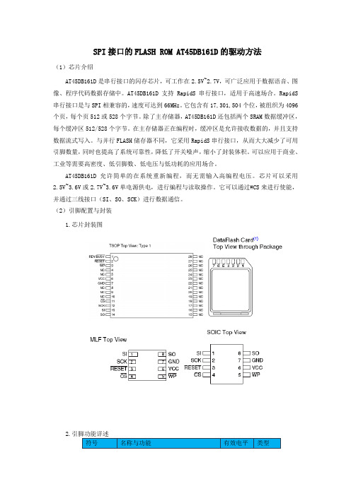
(2)引脚配置与封装1.芯片封装图2.引脚功能详述(3)AT45DB161D的功能框图:(4)存储器阵列:AT45DB161D的储存器阵列被分为3个级别的粒度,分别为扇区、块与页。
下面的“存储器结构图”对各个级别进行了分析,详细说明了每个扇区与块的页数。
所有的编程操作都是针对于页的。
擦除操作可以作用于芯片、扇区、块或页。
扇区结构:块结构:(5)芯片操作:芯片的操作是通过单片机的指令来完成的。
指令列表与指令操作码在后面的“指令表”中有详细的说明。
一个有效的指令由#CS的下降沿来指示它的开始,随后是一个有意义的8位操作码与缓存区或主存储器的地址。
当#CS为低时,由时钟SCK引脚来控制由SI引脚写入的操作码与缓存区或主存储器的地址。
45db041中文特点•单为2.5V - 3.6V的或2.7V - 3.6V电源•串行外设接口(SPI)兼容•页面编程操作- 单周期重新编程(擦除和程序)- 2048页(264字节/页)主存储器•支持页和块擦除操作•两个264字节的SRAM数据缓冲器- 允许接收的数据而重编程非易失性内存•连续读取功能,通过整个阵列•低功耗- 4毫安主动了解当前的典型- 2微安待机电流典型的CMOS•20 MHz的最大时钟频率•硬件数据保护功能•100%兼容AT45DB041和AT45DB041A•5.0V的容错输入:司,SCK的,CS的复位,andWP销•商业和工业温度范围描述该AT45DB041B是2.5伏或2.7伏只,串行接口闪存理想适合的数字语音,图像,程序代码和数据存储的各种申请。
其4325376位存储器的组织264个字节为2048页每个。
除了主内存,AT45DB041B还包含两个SRAM数据每264字节的缓冲区。
缓冲区允许接收数据,同时在页面的主要内存被重新编程,以及读或写一个连续数据流。
EEPROM仿真(位或字节更改性)是很容易处理自包括三个步骤读修改,写操作。
与传统的闪存这是随机访问,与多个地址线和一个并行接口,使用的DataFlash SPI串行接口,以按顺序访问其数据。
数据闪存支持SPI模式0和模式3。
简单的串行接口方便硬件布局,提高了系统的可靠性,减少开关噪声,并减小了封装尺寸和积极引脚数量。
该器件适合用于使用在许多商业和工业应用在高密度,低引脚数,低电压和低功耗是至关重要的。
该器件工作在高达20 MHz的时钟频率读当前一个典型的活跃消费4毫安。
自动页REWRITE这:这种模式只需要如果内一页或多个字节数据多个页面顷修改1随机时尚。
此模式是一组合两个操作:主内存页以缓冲区转移与缓冲区到主存储器佩奇程序与内置擦除。
阿一页数据首先从主内存转入缓冲区1或缓冲区2,然后同一数据从缓冲区1或缓冲区2()被编程放回其主内存原始页面。
#define SPI_GLOBALS#include "config.h"/**************************************************************************** ******函数名称:void SPI_Init( void )****函数描述:SPI接口初始化程序****参 数:无****返 回:无***************************************************************************** *****/void SPI_Init( void ){// 设置硬件SPI的通讯脚: P0.15---SCK, P0.17---MISO, P0.18---MOSI PINSEL0 |= 0xC0000000;PINSEL1 |= 0x0000003C;// MSTR = 1, SPI 处于主模式,8位,CPOL=0,CPHA=0,SPI时钟分频=8S0SPCCR = 0x08; //0x08S0SPCR = 0x20;}/**************************************************************************** ******函数名称:void SPI_Send( uint8 data )****函数描述:SPI接口发送单字节函数****参 数:data---待发送数据****返 回:无***************************************************************************** *****/void SPI_Send( uint8 data ){S0SPDR = data;while ( !(S0SPSR & 0x80) ); // 等待SPIF置位,即等待数据发送完毕S0SPSR = 0; // 清除SPIF标志}/**************************************************************************** ******函数名称:void SPI_Send_nBytes( uint8 *buf, uint32 Length )****函数描述:SPI接口发送多字节函数****参 数:*buf---发送缓冲区 Length---发送字节数****返 回:无***************************************************************************** *****/void SPI_Send_nBytes( uint8 *buf, uint32 Length ){uint32 i;for(i=0; i<Length; i++){SPI_Send(*buf);buf++;}}/**************************************************************************** ******函数名称:uint8 SPI_Recv( void )****函数描述:SPI接口接收单字节函数****参 数:无****返 回:S0SPDR---接收到的数据***************************************************************************** *****/uint8 SPI_Recv( void ){S0SPDR = 0xff;// 发送该数据用以产生时钟,数据本身没有用处while ( !(S0SPSR & 0x80) ); // 等待SPIF置位,即等待数据发送完毕S0SPSR = 0;// 清除SPIF标志return (uint8)(S0SPDR);// 返回接收到的数据}/**********************************************************************************函数名称:void SPI_Recv_nBytes( uint8 *buf, uint32 Length )****函数描述:SPI接口接收多字节函数****参 数:*buf---接收缓冲区 Length---接收字节数****返 回:无**********************************************************************************/void SPI_Recv_nBytes( uint8 *buf, uint32 Length ){uint32 i;for (i=0; i<Length; i++){*buf = SPI_Recv();buf++;}return;}/************************************************************************************************************ End Of File ************************************************************************************************************/。
Features Array•Single 2.5V or 2.7V to 3.6V Supply•RapidS® Serial Interface: 66 MHz Maximum Clock Frequency–SPI Compatible Modes 0 and 3•User Configurable Page Size–256 Bytes per Page–264 Bytes per Page•Page Program Operation–Intelligent Programming Operation–2,048 Pages (256/264 Bytes/Page) Main Memory•Flexible Erase Options–Page Erase (256 Bytes)–Block Erase (2 Kbytes)–Sector Erase (64 Kbytes)–Chip Erase (4 Mbits)•Two SRAM Data Buffers (256/264 Bytes)–Allows Receiving of Data while Reprogramming the Flash Array•Continuous Read Capability through Entire Array–Ideal for Code Shadowing Applications•Low-power Dissipation–7 mA Active Read Current Typical–25 µA Standby Current Typical–5 µA Deep Power-down Typical•Hardware and Software Data Protection Features–Individual Sector•Sector Lockdown for Secure Code and Data Storage–Individual Sector•Security: 128-byte Security Register–64-byte User Programmable Space–Unique 64-byte Device Identifier•JEDEC Standard Manufacturer and Device ID Read•100,000 Program/Erase Cycles Per Page Minimum•Data Retention – 20 Years•Industrial Temperature Range•Green (Pb/Halide-free/RoHS Compliant) Packaging Options1.DescriptionThe AT45DB041D is a 2.5V or 2.7V, serial-interface Flash memory ideally suited for a wide variety of digital voice-, image-, program code- and data-storage applications. The AT45DB041D supports RapidS serial interface for applications requiring very high speed operations. RapidS serial interface is SPI compatible for frequencies up to 66 MHz. Its 4,325,376 bits of memory are organized as 2,048 pages of 256 bytes or 264 bytes each. In addition to the main memory, the AT45DB041D also contains two SRAM buffers of 256/264 bytes each. The buffers allow the receiving of data while a page in the main Memory is being reprogrammed, as well as writing a continuous data stream. EEPROM emulation (bit or byte alterability) is easily handled with a self-con-tained three step read-modify-write operation. Unlike conventional Flash memories that are accessed randomly with multiple address lines and a parallel interface, the DataFlash uses a RapidS serial interface to sequentially access its data. The simplesequential access dramatically reduces active pin count, facilitates hardware layout,23595H–DFLASH–03/07AT45DB041Dincreases system reliability, minimizes switching noise, and reduces package size. The device is optimized for use in many commercial and industrial applications where high-density, low-pin count, low-voltage and low-power are essential.To allow for simple in-system reprogrammability, the AT45DB041D does not require high input voltages for programming. The device operates from a single power supply, 2.5V to 3.6V or 2.7V to 3.6V, for both the program and read operations. The AT45DB041D is enabled through the Serial Output (SO), and the Serial Clock (SCK).All programming and erase cycles are self-timed.2.Pin Configurations and PinoutsTable 2-1.Pin ConfigurationsSymbolName and FunctionAsserted StateTypeCS Chip Select: Asserting the CS pin selects the device. When the CS pin is deasserted, the device will be deselected and normally be placed in the standby mode (not Deep Power-Down mode), and the output pin (SO) will be in a high-impedance state. When the device is deselected, data will not be accepted on the input pin (SI).A high-to-low transition on the CS pin is required to start an operation, and a low-to-high transition is required to end an operation. When ending an internally self-timed operation such as a program or erase cycle, the device will not enter the standby mode until the completion of the operation.Low InputSCK Serial Clock: This pin is used to provide a clock to the device and is used to control the flow of data to and from the device. Command, address, and input data present on the SI pin is always latched on the rising edge of SCK, while output data on the SO pin is always clocked out on the falling edge of SCK.–InputSI Serial Input: The SI pin is used to shift data into the device. The SI pin is used for all data input includingcommand and address sequences. Data on the SI pin is always latched on the rising edge of SCK. If the SER/BYTE pin is always driven low, the SI pin should be a “no connect”.–InputSO Serial Output: The SO pin is used to shift data out from the device. Data on the SO pin is always clocked out on the falling edge of SCK. If the SER/BYTE pin is always driven low, the SO pin should be a “no connect”.–OutputWPWrite Protect: When the WP pin is asserted, all sectors specified for protection by the Sector Protection Register will be protected against program and erase operations regardless of whether the Enable Sector Protection command has been issued or not. The WP pin functions independently of the software controlled protection method. After the WP pin goes low, the content of the Sector Protection Register cannot be modified.If a program or erase command is issued to the device while the WP pin is asserted, the device will simply ignore the command and perform no operation. The device will return to the idle state once the CS pin has been deasserted. The Enable Sector Protection command and Sector Lockdown command, however, will be recognized by the device when the WP pin is asserted.The WP pin is internally pulled-high and may be left floating if hardware controlled protection will not be used. However, it is recommended that the WP pin also be externally connected to V CC whenever possible.Low InputRESET Reset: A low state on the reset pin (RESET) will terminate the operation in progress and reset the internal state machine to an idle state. The device will remain in the reset condition as long as a low level is present on the RESET pin. Normal operation can resume once the RESET pin is brought back to a high level.The device incorporates an internal power-on reset circuit, so there are no restrictions on the RESET pin during power-on sequences. If this pin and feature are not utilized it is recommended that the RESET pin be driven high externally.Low InputV CC Device Power Supply: The V CC pin is used to supply the source voltage to the device.Operations at invalid V CC voltages may produce spurious results and should not be attempted.–Power GNDGround: The ground reference for the power supply. GND should be connected to the system ground.–Ground33595H–DFLASH–03/07AT45DB041D3.Block DiagramFigure 2-1.MLF Top ViewFigure 2-2.SOIC Top View43595H–DFLASH–03/07AT45DB041D4.Memory ArrayTo provide optimal flexibility, the memory array of the AT45DB041D is divided into three levels of granularity comprising of sectors, blocks, and pages. The “Memory Architecture Diagram” illus-trates the breakdown of each level and details the number of pages per sector and block. All program operations to the DataFlash occur on a page-by-page basis. The erase operations can be performed at the chip, sector, block or page level.Figure 4-1.Memory Architecture Diagram5.Device OperationThe device operation is controlled by instructions from the host processor. The list of instructions and their associated opcodes are contained in Tables 15-1 through 15-7. A valid instruction starts with the falling edge of CS followed by the appropriate 8-bit opcode and the desired buffer loading of the opcode and the desired buffer or main memory address location through the SI (serial input) pin. All instructions, addresses, and data are transferred with the most significant bit (MSB) first.Buffer addressing for the DataFlash standard page size (264 bytes) is referenced in the datasheet using the terminology BEA8 - BFA0 to denote the 9 address bits required to designate a byte address within a buffer. Main memory addressing is referenced using the terminology PA10 - PA0 and BA8 - BA0, where PA10 - PA0 denotes the 11 address bits required to desig-nate a page address and BA8 - BA0 denotes the 9 address bits required to designate a byte address within the page.For the “Power of 2” binary page size (256 bytes), the Buffer addressing is referenced in the datasheet using the conventional terminology BFA7 - BFA0 to denote the 8 address bits required to designate a byte address within a buffer. Main memory addressing is referenced using the terminology A18 - A0, where A18 - A8 denotes the 11 address bits required to desig-nate a page address and A7 - A0 denotes the 8 address bits required to designate a byte address within a page.53595H–DFLASH–03/07AT45DB041D6.Read CommandsBy specifying the appropriate opcode, data can be read from the main memory or from either one of the two SRAM data buffers. The DataFlash supports RapidS protocols for Mode 0 and Mode 3. Please refer to the “Detailed Bit-level Read Timing” diagrams in this datasheet for details on the clock cycle sequences for each mode.6.1Continuous Array Read (Legacy Command – E8H): Up to 66 MHzBy supplying an initial starting address for the main memory array, the Continuous Array Read command can be utilized to sequentially read a continuous stream of data from the device by simply providing a clock signal; no additional addressing information or control signals need to be provided. The DataFlash incorporates an internal address counter that will automatically increment on every clock cycle, allowing one continuous read operation without the need of additional address sequences. To perform a continuous read from the DataFlash standard page size (264 bytes), an opcode of E8H must be clocked into the device followed by three address bytes (which comprise the 24-bit page and byte address sequence) and 4 don’t care bytes. The first 11 bits (PA10-PA0) of the 20-bit address sequence specify which page of the main mem-ory array to read, and the last 9 bits (BA8-BA0) of the 20-bit address sequence specify the starting byte address within the page. To perform a continuous read from the binary page size (256 bytes), the opcode (E8H) must be clocked into the device followed by three address bytes and 4 don’t care bytes. The first 11 bits (A18 - A8) of the 19-bits sequence specify which page of the main memory array to read, and the last 8 bits (A7 - A0) of the 19-bits address sequence specify the starting byte address within the page. The don’t care bytes that follow the address bytes are needed to initialize the read operation. Following the don’t care bytes, additional clock pulses on the SCK pin will result in data being output on the SO (serial output) pin.The CS pin must remain low during the loading of the opcode, the address bytes, the don’t care bytes, and the reading of data. When the end of a page in main memory is reached during a Continuous Array Read, the device will continue reading at the beginning of the next page with no delays incurred during the page boundary crossover (the crossover from the end of one page to the beginning of the next page). When the last bit in the main memory array has been read,the device will continue reading back at the beginning of the first page of memory. As with cross-ing over page boundaries, no delays will be incurred when wrapping around from the end of the array to the beginning of the array.pin (SO). The maximum SCK frequency allowable for the Continuous Array Read is defined by the f CAR1 specification. The Continuous Array Read bypasses both data buffers and leaves the contents of the buffers unchanged.6.2Continuous Array Read (High Frequency Mode – 0BH): Up to 66 MHzThis command can be used with the serial interface to read the main memory array sequentially in high speed mode for any clock frequency up to the maximum specified by f CAR1. To perform a opcode 0BH must be clocked into the device followed by three address bytes and a dummy byte. The first 11 bits (PA10 - PA0) of the 20-bit address sequence specify which page of the main memory array to read, and the last 9 bits (BA8 - BA0) of the 20-bit address sequence spec-ify the starting byte address within the page. To perform a continuous read with the page size set to 256 bytes, the opcode, 0BH, must be clocked into the device followed by three address bytes (A18 - A0) and a dummy byte. Following the dummy byte, additional clock pulses on the SCK pin will result in data being output on the SO (serial output) pin.63595H–DFLASH–03/07AT45DB041DThe CS pin must remain low during the loading of the opcode, the address bytes, and the read-ing of data. When the end of a page in the main memory is reached during a Continuous Array Read, the device will continue reading at the beginning of the next page with no delays incurred during the page boundary crossover (the crossover from the end of one page to the beginning of the next page). When the last bit in the main memory array has been read, the device will con-tinue reading back at the beginning of the first page of memory. As with crossing over page boundaries, no delays will be incurred when wrapping around from the end of the array to the beginning of the array. A low-to-high transition on the CS pin will terminate the read operation and tri-state the output pin (SO). The maximum SCK frequency allowable for the Continuous Array Read is defined by the f CAR1 specification. The Continuous Array Read bypasses both data buffers and leaves the contents of the buffers unchanged.6.3Continuous Array Read (Low Frequency Mode: 03H): Up to 33 MHzThis command can be used with the serial interface to read the main memory array sequentially without a dummy byte up to maximum frequencies specified by f CAR2. To perform a continuous 03H, must be clocked into the device followed by three address bytes (which comprise the 24-bit page and byte address sequence). The first 11 bits (PA10 - PA0) of the 20-bit address sequence specify which page of the main memory array to read, and the last 9 bits (BA8 - BA0) of the 20-bit address sequence specify the starting byte address within the page. To perform a contin-uous read with the page size set to 256 bytes, the opcode, 03H, must be clocked into the device followed by three address bytes (A18 - A0). Following the address bytes, additional clock pulses on the SCK pin will result in data being output on the SO (serial output) pin.The CS pin must remain low during the loading of the opcode, the address bytes, and the read-ing of data. When the end of a page in the main memory is reached during a Continuous Array Read, the device will continue reading at the beginning of the next page with no delays incurred during the page boundary crossover (the crossover from the end of one page to the beginning of the next page). When the last bit in the main memory array has been read, the device will con-tinue reading back at the beginning of the first page of memory. As with crossing over page boundaries, no delays will be incurred when wrapping around from the end of the array to the beginning of the array. A low-to-high transition on the CS pin will terminate the read operation and tri-state the output pin (SO). The Continuous Array Read bypasses both data buffers and leaves the contents of the buffers unchanged.6.4Main Memory Page ReadA main memory page read allows the user to read data directly from any one of the 2,048 pages in the main memory, bypassing both of the data buffers and leaving the contents of the buffers unchanged. To start a page read from the DataFlash standard page size (264 bytes), an opcode of D2H must be clocked into the device followed by three address bytes (which comprise the 24-bit page and byte address sequence) and 4 don’t care bytes. The first 11 bits (PA10-PA0) of the 20-bit address sequence specify the page in main memory to be read, and the last 9 bits (BA8-BA0) of the 20-bit address sequence specify the starting byte address within that page.To start a page read from the binary page size (256 bytes), the opcode D2H must be clocked into the device followed by three address bytes and 4 don’t care bytes. The first 11 bits (A18 - A8) of the 19-bits sequence specify which page of the main memory array to read, and the last 8 bits (A7 - A0) of the 19-bits address sequence specify the starting byte address within the page. The don’t care bytes that follow the address bytes are sent to initialize the read opera-tion. Following the don’t care bytes, additional pulses on SCK result in data being output on the SO (serial output) pin. The CS pin must remain low during the loading of the opcode, the address bytes, the don’t care bytes, and the reading of data. When the end of a page in main73595H–DFLASH–03/07AT45DB041Dmemory is reached, the device will continue reading back at the beginning of the same page. A low-to-high transition on the CS pin will terminate the read operation and tri-state the output pin (SO). The maximum SCK frequency allowable for the Main Memory Page Read is defined by the f SCK specification. The Main Memory Page Read bypasses both data buffers and leaves the contents of the buffers unchanged.6.5Buffer ReadThe SRAM data buffers can be accessed independently from the main memory array, and utiliz-ing the Buffer Read Command allows data to be sequentially read directly from the buffers. Four opcodes, D4H or D1H for buffer 1 and D6H or D3H for buffer 2 can be used for the Buffer Read Command. The use of each opcode depends on the maximum SCK frequency that will be used to read data from the buffer. The D4H and D6H opcode can be used at any SCK frequency up to the maximum specified by f CAR1. The D1H and D3H opcode can be used for lower frequency read operations up to the maximum specified by f CAR2.To perform a buffer read from the DataFlash standard buffer (264 bytes), the opcode must be clocked into the device followed by three address bytes comprised of 15 don’t care bits and 9buffer address bits (BFA8-BFA0). To perform a buffer read from the binary buffer (256 bytes),the opcode must be clocked into the device followed by three address bytes comprised of 16don’t care bits and 8 buffer address bits (BFA7 - BFA0). Following the address bytes, one don’t care byte must be clocked in to initialize the read operation. The CS pin must remain low during the loading of the opcode, the address bytes, the don’t care bytes, and the reading of data. When the end of a buffer is reached, the device will continue reading back at the beginning the output pin (SO).7.Program and Erase Commands7.1Buffer WriteData can be clocked in from the input pin (SI) into either buffer 1 or buffer 2. To load data into the DataFlash standard buffer (264 bytes), a 1-byte opcode, 84H for buffer 1 or 87H for buffer 2,must be clocked into the device, followed by three address bytes comprised of 15 don’t care bits and 9 buffer address bits (BFA8-BFA0). The 9 buffer address bits specify the first byte in the buffer to be written. To load data into the binary buffers (256 bytes each), a 1-byte opcode 84H for buffer 1 or 87H for buffer 2, must be clocked into the device, followed by three address bytes comprised of 16 don’t care bits and 8 buffer address bits (BFA7 - BFA0). The 8 buffer address bits specify the first byte in the buffer to be written. After the last address byte has been clocked into the device, data can then be clocked in on subsequent clock cycles. If the end of the data buffer is reached, the device will wrap around back to the beginning of the buffer. Data will con-7.2Buffer to Main Memory Page Program with Built-in EraseData written into either buffer 1 or buffer 2 can be programmed into the main memory. A 1-byte opcode, 83H for buffer 1 or 86H for buffer 2, must be clocked into the device. For the DataFlash standard page size (264 bytes), the opcode must be followed by three address bytes consist of 4 don’t care bits, 11 page address bits (PA10 - PA0) that specify the page in the main memory to be written and 9 don’t care bits. To perform a buffer to main memory page program with built-in erase for the binary page size (256 bytes), the opcode 83H for buffer 1 or 86H for buffer 2, must be clocked into the device followed by three address bytes consisting of 5 don’t care bits83595H–DFLASH–03/07AT45DB041D11page address bits (A18 - A8) that specify the page in the main memory to be written and 8don’t care bits. When a low-to-high transition occurs on the CS pin, the part will first erase the selected page in main memory (the erased state is a logic 1) and then program the data stored in the buffer into the specified page in main memory. Both the erase and the programming of the page are internally self-timed and should take place in a maximum time of t EP . During this time,the status register will indicate that the part is busy.7.3Buffer to Main Memory Page Program without Built-in EraseA previously-erased page within main memory can be programmed with the contents of either buffer 1 or buffer 2. A 1-byte opcode, 88H for buffer 1 or 89H for buffer 2, must be clocked into the device. For the DataFlash standard page size (264 bytes), the opcode must be followed by three address bytes consist of 4 don’t care bits, 11 page address bits (PA10-PA0) that specify the page in the main memory to be written and 9 don’t care bits. To perform a buffer to main memory page program without built-in erase for the binary page size (256 bytes), the opcode 88H for buffer 1 or 89H for buffer 2, must be clocked into the device followed by three address bytes consisting of 5 don’t care bits, 11 page address bits (A18 - A8) that specify the page in the main memory to be written and 8 don’t care bits. When a low-to-high transition occurs on the CS pin, the part will program the data stored in the buffer into the specified page in the main mem-ory. It is necessary that the page in main memory that is being programmed has been previously erased using one of the erase commands (Page Erase or Block Erase). The programming of the page is internally self-timed and should take place in a maximum time of t P . During this time, the status register will indicate that the part is busy.7.4Page EraseThe Page Erase command can be used to individually erase any page in the main memory array allowing the Buffer to Main Memory Page Program to be utilized at a later time. To perform a page erase in the DataFlash standard page size (264bytes), an opcode of 81H must be loaded into the device, followed by three address bytes comprised of 4 don’t care bits, 11 page address bits (PA10-PA0) that specify the page in the main memory to be erased and 9 don’t care bits.To perform a page erase in the binary page size (256 bytes), the opcode 81H must be loaded into the device, followed by three address bytes consist of 5 don’t care bits, 11 page address bits (A18 - A8) that specify the page in the main memory to be erased and 8 don’t care bits. When a state is a logical 1). The erase operation is internally self-timed and should take place in a maxi-mum time of t PE . During this time, the status register will indicate that the part is busy.7.5Block EraseA block of eight pages can be erased at one time. This command is useful when large amounts of data has to be written into the device. This will avoid using multiple Page Erase Commands.To perform a block erase for the DataFlash standard page size (264bytes), an opcode of 50H must be loaded into the device, followed by three address bytes comprised of 4 don’t care bits,8page address bits (PA10 - PA3) and 12 don’t care bits. The 8 page address bits are used to specify which block of eight pages is to be erased. To perform a block erase for the binary page size (256 bytes), the opcode 50H must be loaded into the device, followed by three address bytes consisting of 5 don’t care bits, 8 page address bits (A18 - A11) and 11 don’t care bits. The 9 page address bits are used to specify which block of eight pages is to be erased. When a low-to-high transition occurs on the CS pin, the part will erase the selected block of eight pages. The erase operation is internally self-timed and should take place in a maximum time of t BE . During this time, the status register will indicate that the part is busy.93595H–DFLASH–03/07AT45DB041D7.6Sector EraseThe Sector Erase command can be used to individually erase any sector in the main memory.There are 8 sectors and only one sector can be erased at one time. To perform sector 0a or sec-tor 0b erase for the DataFlash standard page size (264 bytes), an opcode of 7CH must be loaded into the device, followed by three address bytes comprised of 4 don’t care bits, 8 page address bits (PA10 - PA3) and 12 don’t care bits. To perform a sector 1-7 erase, the opcode 7CH must be loaded into the device, followed by three address bytes comprised of 4 don’t care bits, 3 page address bits (PA10 - PA8) and 17 don’t care bits. To perform sector 0a or sector 0b erase for the binary page size (256 bytes), an opcode of 7CH must be loaded into the device,followed by three address bytes comprised of 5 don’t care bit and 8 page address bits (A18 -A11) and 11 don’t care bits. To perform a sector 1-15 erase, the opcode 7CH must be loaded into the device, followed by three address bytes comprised of 5 don’t care bit and 3 page address bits (A18 - A16) and 17 don’t care bits. The page address bits are used to specify any valid address location within the sector which is to be erased. When a low-to-high transition self-timed and should take place in a maximum time of t SE . During this time, the status register will indicate that the part is busy.Table 7-1.Block Erase AddressingPA10/A18PA9/A17PA8/A16PA7/A15PA6/A14PA5/A13PA4/A12PA3/A11PA2/A10PA1/A9PA0/A8Block 00000000X X X 000000001X X X 100000010X X X 200000011X X X 3••••••••••••••••••••••••••••••••••••11111100X X X 25211111101X X X 25311111110X X X 25411111111XXX255103595H–DFLASH–03/07AT45DB041D7.7Chip Erase (1)The entire main memory can be erased at one time by using the Chip Erase command.To execute the Chip Erase command, a 4-byte command sequence C7H, 94H, 80H and 9AH must be clocked into the device. Since the entire memory array is to be erased, no address bytes need to be clocked into the device, and any data clocked in after the opcode will be ignored. After the last bit of the opcode sequence has been clocked in, the CS pin can be deas-serted to start the erase process. The erase operation is internally self-timed and should take place in a time of t CE . During this time, the Status Register will indicate that the device is busy.The Chip Erase command will not affect sectors that are protected or locked down; the contents of those sectors will remain unchanged. Only those sectors that are not protected or locked down will be erased.The WP pin can be asserted while the device is erasing, but protection will not be activated until the internal erase cycle completes.Figure 7-1.Chip EraseNote: 1.Refer to the errata regarding Chip Erase on page 52.Table 7-2.Sector Erase AddressingPA10/A18PA9/A17PA8/A16PA7/A15PA6/A14PA5/A13PA4/A12PA3/A11PA2/A10PA1/A9PA0/A8Sector 00000000X X X 0a 00000001X X X 0b 001X X X X X X X X 1010X X X X X X X X 2••••••••••••••••••••••••••••••••••••100X X X X X X X X 4101X X X X X X X X 5110X X X X X X X X 6111XXXXXXXX7Command Byte 1Byte 2Byte 3Byte 4Chip EraseC7H94H80H9AHAT45DB041D7.8Main Memory Page Program Through BufferThis operation is a combination of the Buffer Write and Buffer to Main Memory Page Programwith Built-in Erase operations. Data is first clocked into buffer 1 or buffer 2 from the input pin (SI)and then programmed into a specified page in the main memory. To perform a main memorypage program through buffer for the DataFlash standard page size (264 bytes), a 1-byte opcode,82H for buffer 1 or 85H for buffer 2, must first be clocked into the device, followed by threeaddress bytes. The address bytes are comprised of 4 don’t care bits, 11 page address bits,(PA10-PA0) that select the page in the main memory where data is to be written, and 9 bufferaddress bits (BFA8-BFA0) that select the first byte in the buffer to be written. To perform amain memory page program through buffer for the binary page size (256 bytes), the opcode 82Hfor buffer 1 or 85H for buffer 2, must be clocked into the device followed by three address bytesconsisting of 5 don’t care bits, 11 page address bits (A18 - A8) that specify the page in the mainmemory to be written, and 8 buffer address bits (BFA7 - BFA0) that selects the first byte in thebuffer to be written. After all address bytes are clocked in, the part will take data from the inputpins and store it in the specified data buffer. If the end of the buffer is reached, the device willpin, the part will first erase the selected page in main memory to all 1s and then program thedata stored in the buffer into that memory page. Both the erase and the programming of thepage are internally self-timed and should take place in a maximum time of t EP. During this time,the status register will indicate that the part is busy.8.Sector ProtectionTwo protection methods, hardware and software controlled, are provided for protection againstinadvertent or erroneous program and erase cycles. The software controlled method relies onthe use of software commands to enable and disable sector protection while the hardware con-that are to be protected or unprotected against program and erase operations is specified in thenonvolatile Sector Protection Register. The status of whether or not sector protection has beenenabled or disabled by either the software or the hardware controlled methods can be deter-mined by checking the Status Register.。
AT45DB321D资料总结存储空间:4MB;8192页,每页512个字节或者528个字节(向AT45DB发送0x3D,0x2A,0x80,0xA6可设置为528字节。
默认512字节,但是选择了528字节便无法再设置成512字节了)。
每页512字节地址分配:buffer1,buffer2缓冲区地址:BFA8 BFA7 BFA6 BFA5 BFA4 BFA3 BFA2 BFA1 BFA0页地址:A21 A20 A19 A18 A17 A16 A15 A14 A13 A12 A10 A9每页当中数据地址:A8 A7 A6 A5 A4 A3 A2 A1 A0每页528字节地址分配:buffer1、buffer2缓冲区地址:BFA9 BFA8 BFA7 BFA6 BFA5 BFA4 BFA3 BFA2 BFA1 BFA0页地址:PA12 PA11 PA10 PA9 PA8 PA7 PA6 PA5 PA4 PA3 PA2 PA1 PA0每页当中数据地址:BA9 BA8 BA7 BA6 BA5 BA4 BA3 BA2 BA1 BA0读45DB过程:步骤功能操作备注第一步将存储器中的数据读到buffer1或者buffer2中去依次发送0x53,page_adder>>6,page_adder<<2,0x00或者发送0x55,page_adder>>6,page_adder<<2,0x001、0x53代表将buffer1中的数据写入存储器;2、0x55代表将buffer2中的数据写入存储器;3、page_adder>>6、page_adder<<2详情请看注解4、0x00不必关心;第二步读取状态寄存器发送0x57 1、发送完之后读取45DB返回的值最高位是不是1,是则执行下一步,不是则继续读第三步读取buffer1或者buffer2中的数据依次发送0x54,0x00,buff_adder_h,buff_adder_l,0x00或者发送0x56,0x00,buff_adder_h,buff_adder_l,0x001、0x54代表读取buffer1中的数据;2、0x56代表读取buffer2中的数据;3、adder_h,adder_l分别是buffer1或者buffer2地址高位和低位;4、0x00不必关心;第四步接收数据单片机接收MISO口收到的数据写45DB过程步骤功能操作备注第一步将存储器中的数据读到buffer1或者buffer2中去依次发送0x53,page_adder>>6,page_adder<<2,0x00或者发送0x55,page_adder>>6,page_adder<<2,0x001、0x53代表将buffer1中的数据写入存储器;2、0x55代表将buffer2中的数据写入存储器;3、page_adder>>6、page_adder<<2详情请看注解4、0x00不必关心;第二步将数据写到buffer1或者buffer2中去依次发送0x84,0x00,buff_adder_h,buff_adder_l,data或者发送0x87,0x00,buff_adder_h,buff_adder_l,data1、0x84代表写到buffer1;2、0x87代表写到buffer2;3、adder_h,adder_l分别是数据在buffer1或者buffer2中地址的高位和低位;4、0x00不必关心;5、data为依次发出的数据。