常用电源芯片使用 PPT
- 格式:ppt
- 大小:1.12 MB
- 文档页数:35

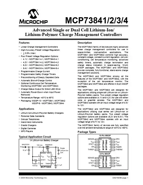
2004 Microchip Technology Inc.DS21823B-page 1MMCP73841/2/3/4Features•Linear Charge Management Controllers •High-Accuracy Preset Voltage Regulation:-+ 0.5% (max)•Four Preset Voltage Regulation Options:- 4.1V - MCP73841-4.1, MCP73843-4.1- 4.2V - MCP73841-4.2, MCP73843-4.2-8.2V - MCP73842-8.2, MCP73844-8.2-8.4V - MCP73842-8.4, MCP73844-8.4•Programmable Charge Current•Programmable Safety Charge Timers •Preconditioning of Deeply Depleted Cells •Automatic End-of-Charge Control•Optional Continuous Cell Temperature Monitoring (MCP73841 and MCP73842)•Charge Status Output for Direct LED Drive •Automatic Power-Down when Input Power Removed•T emperature Range: -40°C to 85°C•Packaging: MSOP-10 - MCP73841, MCP73842MSOP-8 - MCP73843, MCP73844Applications•Lithium-Ion/Lithium-Polymer Battery Chargers •Personal Data Assistants •Cellular Telephones •Hand-Held Instruments •Cradle Chargers •Digital Cameras •MP3 PlayersTypical Application CircuitDescriptionThe MCP7384X family of devices are highly advanced linear charge management controllers for use in space-limited, cost-sensitive applications. The MCP73841 and MCP73842 combine high accuracy,constant-voltage, constant-current regulation, cell pre-conditioning, cell temperature monitoring, advanced safety timers, automatic charge termination and charge status indication in space-saving, 10-pin MSOP packages. The MCP73841 and MCP73842provide complete, fully-functional, stand-alone charge management solutions.The MCP73843 and MCP73844 employ all the features of the MCP73841 and MCP73842, with the exception of the cell temperature monitor. The MCP73843 and MCP73844 are offered in 8-pin MSOP packages.The MCP73841 and MCP73843 are designed for applications utilizing single-cell Lithium-Ion or Lithium-Polymer battery packs. Two preset voltage regulation options are available (4.1V and 4.2V) for use with either coke or graphite anodes. The MCP73841 and MCP73843 operate with an input voltage range of 4.5V to 12V.The MCP73842 and MCP73844 are designed for applications utilizing dual series cell Lithium-Ion or Lithium-Polymer battery packs. Two preset voltage regulation options are available (8.2V and 8.4V). The MCP73842 and MCP73844 operate with an input voltage range of 8.7V to 12V.The MCP7384X family of devices are fully specified over the ambient temperature range of -40°C to +85°C.Package Types+-V SS DRV SENSE V DD V BATSTAT136712MCP73843810µF10µF 100k Ω100m Ω5V SingleLithium-Ion CellNDS8434MA2Q7051A Lithium-Ion Battery ChargerEN5TIMER40.1µF10-Pin MSOPSENSEV DD STAT1ENDRV V BAT V SS TIMER12348765M C P 73843M C P 738448-Pin MSOPV DD STAT1EN THREFV BAT V SS TIMER THERM23459876M C P 73841M C P 73842SENSEDRV 110Advanced Single or Dual Cell Lithium-Ion/Lithium-Polymer Charge Management ControllersMCP73841/2/3/4DS21823B-page 2 2004 Microchip Technology Inc.Functional Block DiagramCharge Termination Comparator Voltage Control AmplifierV REFI REG /10Precondition ControlCharge_ok PreconV DDCharge Current Control Amplifier+–V REF V REFPrecondition Comp .V BAT V SS DRV90k Ω90k Ω10k Ω10k Ω+–Charge Current AmplifierV DD SENSEMCP73841 and MCP73842 Only300k Ω (825k Ω)12k Ω1k ΩUVLOComparatorV UVLOT emperature ComparatorsBias and Reference GeneratorV UVLOV REF (1.2V)Power-On DelayV REFOscillatorConstant-Voltage/ Recharge Comp.Charge Control, Charge Timers,And Status LogicDrv Stat 1Charge_okI REG /10THERMENTIMERSTAT1THREF100k Ω50k Ω50k Ω74.21k Ω0.79k Ω150.02k Ω5.15k Ω (4.29k Ω)+-+-+-+-+-+-+-MCP73841/2/3/41.0ELECTRICALCHARACTERISTICSAbsolute Maximum Ratings†V DD.................................................................................13.5V All inputs and outputs w.r.t. V SS................-0.3 to (V DD+0.3)V Current at DRV Pin ......................................................±4mA Current at STAT1 Pin .................................................±30mA Maximum Junction Temperature, T J.............................150°C Storage temperature.....................................-65°C to +150°C ESD protection on all pins:Human Body Model (1.5kΩ in Series with 100pF).......≥ 2kV Machine Model (200pF, No Series Resistance).............200V *Notice: Stresses above those listed under “Maximum Ratings” may cause permanent damage to the device. This is a stress rating only and functional operation of the device at those or any other conditions above those indicated in the operational listings of this specification is not implied. Expo-sure to maximum rating conditions for extended periods may affect device reliability.DC CHARACTERISTICSElectrical Specifications: Unless otherwise indicated, all limits apply for V DD= [V REG(Typ)+0.3V] to 12V, T A = -40°C to +85°C. Typical values are at +25°C, V DD = [V REG(Typ) + 1V].Parameters Sym Min Typ Max Units ConditionsSupply InputSupply Voltage V DDMCP73841, MCP73843 4.5–12VMCP73842, MCP738448.7–12VSupply Current I SS––0.250.7544µAmADisabledOperatingV DD =V REG(Typ)+1VUVLO Start Threshold V STARTMCP73841, MCP73843 4.25 4.45 4.60V V DD Low-to-High MCP73842, MCP738448.458.658.90V V DD Low-to-High UVLO Stop Threshold V STOPMCP73841, MCP73843 4.20 4.40 4.55V V DD High-to-Low MCP73842, MCP738448.408.608.85V V DD High-to-Low Voltage Regulation (Constant-Voltage Mode)Regulated Output Voltage V REGMCP73841-4.1, MCP73843-4.14.079 4.1 4.121V V DD = [V REG(Typ)+1V], I OUT = 10mA,T A = -5°C to +55°CMCP73841-4.2, MCP73843-4.24.179 4.2 4.221V V DD = [V REG(Typ)+1V], I OUT = 10mA,T A = -5°C to +55°CMCP73842-8.2, MCP73844-8.28.1598.28.241V V DD = [V REG(Typ)+1V], I OUT = 10mA,T A = -5°C to +55°CMCP73842-8.4, MCP73844-8.48.3588.48.442V V DD = [V REG(Typ)+1V], I OUT = 10mA,T A = -5°C to +55°CLine Regulation|(∆V BAT/V BAT)|/∆V DD –0.0250.25%/V V DD = [V REG(Typ)+1V] to 12V,I OUT = 10mALoad Regulation|∆V BAT|/V BAT–0.010.25%I OUT = 10mA to 150mA,V DD = [V REG(Typ)+1V]Supply Ripple Attenuation PSRR–-58–dB I OUT = 10mA, 100Hz–-42–dB I OUT = 10mA, 1kHz–-30–dB I OUT = 10mA, 10kHzOutput Reverse LeakageCurrentI DISCHARGE–0.41µA V DD Floating, V BAT = V REG(Typ) Current Regulation (Fast Charge Constant-Current Mode)Fast Charge Current Regulation Threshold V FCS100110120mV V DD – V SENSE,T A = -5°C to +55°C2004 Microchip Technology Inc.DS21823B-page 3MCP73841/2/3/4DS21823B-page 4 2004 Microchip Technology Inc.Preconditioning Current Regulation (Trickle Charge Constant-Current Mode)Precondition Current Regulation ThresholdV PCS 51015mVV DD – V SENSE,T A = -5°C to +55°CPrecondition Threshold VoltageV PTHMCP73841-4.1,MCP73843-4.1 2.70 2.80 2.90V V BAT Low-to-High MCP73841-4.2,MCP73843-4.2 2.75 2.85 2.95V V BAT Low-to-High MCP73842-8.2,MCP73844-8.2 5.40 5.60 5.80V V BAT Low-to-High MCP73842-8.4,MCP73844-8.4 5.505.705.90VV BAT Low-to-HighCharge TerminationCharge Termination Threshold V TCS4710mVV DD – V SENSE,T A = -5°C to +55°CAutomatic Recharge Recharge Threshold VoltageV RTHMCP73841,MCP73843V REG -300mV V REG -200mV V REG -100mV V V BAT High-to-Low MCP73842,MCP73844V REG -600mV V REG -400mV V REG -200mVVV BAT High-to-LowExternal MOSFET Gate Drive Gate Drive CurrentI DRV –2–mA Sink, CV Mode –-0.5–mA Source, CV Mode Gate Drive Minimum Voltage V DRVMIN –– 1.0V V DD = 4.5V Gate - Source Clamp Voltage V GS -7.0–-4.5V V DD = 12.0VThermistor Reference - MCP73841, MCP73842Thermistor Reference Output VoltageV THREF 2.475 2.55 2.625V T A = +25°C, V DD = V REG (Typ)+1V,I THREF = 0mAT emperature Coefficient TC THREF –+50–ppm/°C Thermistor Reference Source CurrentI THREF 200––µA Thermistor Reference Line Regulation|(∆V THREF /V THREF )|/∆V DD –0.10.25%/VV DD =[V REG (Typ)+1V] to 12V Thermistor Reference Load Regulation∆V THREF /V THREF–0.010.10%I THREF = 0mA to 0.20mAThermistor Comparator - MCP73841, MCP73842Upper Trip Threshold V T1 1.18 1.25 1.32V Upper Trip Point Hysteresis V T1HYS –-50–mV Lower Trip Threshold V T20.590.620.66V Lower Trip Point Hysteresis V T2HYS –80–mV Input Bias Current |I BIAS |––2µAStatus Indicator Sink Current I SINK 4712mA Low Output Voltage V OL –200400mV I SINK = 1mAInput Leakage CurrentI LK–0.011µAI SINK = 0mA, V STAT1 = 12VDC CHARACTERISTICS (CONTINUED)Electrical Specifications: Unless otherwise indicated, all limits apply for V DD = [V REG (Typ)+0.3V] to 12V, T A = -40°C to +85°C.Typical values are at +25°C, V DD = [V REG (Typ) + 1V].ParametersSym Min Typ Max Units Conditions2004 Microchip Technology Inc.DS21823B-page 5MCP73841/2/3/4AC CHARACTERISTICSTEMPERATURE SPECIFICATIONSEnable InputInput High-Voltage Level V IH 1.4-–V Input Low-Voltage Level V IL –-0.8V Input Leakage CurrentI LK–0.011µAV ENABLE = 12VElectrical Specifications: Unless otherwise indicated, all limits apply for V DD = [V REG (Typ)+0.3V] to 12V, T A = -40°C to +85°C. Typ-ical values are at +25°C, V DD = [V REG (Typ)+1V].ParametersSym Min Typ Max Units ConditionsUVLO Start Delay t START––5msecV DD Low-to-HighCurrent Regulation Transition Time Out of Preconditioningt DELAY ––1msec V BAT < V PTH to V BAT > V PTH Current Rise Time Out of Preconditioningt RISE ––1msec I OUT Rising to 90% of I REG Fast Charge Safety Timer Period t FAST1.21.41.6HoursC TIMER = 0.1µFPreconditioning Current Regulation Preconditioning Charge Safety Timer Period t PRECON506070MinutesC TIMER = 0.1µFCharge TerminationElapsed Time Termination Period t TERM2.52.93.3HoursC TIMER = 0.1µFStatus Indicators Status Output turn-off t OFF ––200µsec I SINK = 10mA to 0mA Status Output turn-ont ON––200µsecI SINK = 0mA to 10mAElectrical Specifications: Unless otherwise specified, all limits apply for V DD = [V REG (Typ)+0.3V] to 12V.Typical values are at +25°C, V DD = [V REG (Typ)+1.0V].ParametersSymMinTypMaxUnitsConditionsTemperature Ranges Specified Temperature Range T A -40+85°C Operating Temperature Range T A -40+125°C Storage T emperature Range T A-65+150°CThermal Package Resistances Thermal Resistance, MSOP-10θJA 113°C/W 4-Layer JC51-7 Standard Board, Natural ConvectionThermal Resistance, MSOP-8θJA206°C/WSingle-Layer SEMI G42-88 Board, Natural ConvectionDC CHARACTERISTICS (CONTINUED)Electrical Specifications: Unless otherwise indicated, all limits apply for V DD = [V REG (Typ)+0.3V] to 12V, T A = -40°C to +85°C.Typical values are at +25°C, V DD = [V REG (Typ) + 1V].ParametersSymMinTypMaxUnitsConditionsMCP73841/2/3/4DS21823B-page 6 2004 Microchip Technology Inc.2.0TYPICAL PERFORMANCE CURVESNote: Unless otherwise indicated, V DD = [V REG (Typ) + 1V], I OUT = 10mA and T A = +25°C.FIGURE 2-1:Battery Regulation Voltage (V BAT ) vs. Charge Current (I OUT ).FIGURE 2-2:Battery Regulation Voltage (V BAT ) vs. Supply Voltage (V DD ).FIGURE 2-3:Battery Regulation Voltage (V BAT ) vs. Supply Voltage (V DD ).FIGURE 2-4:Supply Current (I SS ) vs. Charge Current (I OUT ).FIGURE 2-5:Supply Current (I SS ) vs. Supply Voltage (V DD ).FIGURE 2-6:Supply Current (I SS ) vs. Supply Voltage (V DD ).Note:The graphs and tables provided following this note are a statistical summary based on a limited number of samples and are provided for informational purposes only. The performance characteristics listed herein are not tested or guaranteed. In some graphs or tables, the data presented may be outside the specified operating range (e.g., outside specified power supply range) and therefore outside the warranted range.MCP73841/2/3/4 Note: Unless otherwise indicated, V DD = [V REG(Typ) + 1V], I OUT = 10mA and T A= +25°C.FIGURE 2-7:Battery Regulation Voltage (V BAT) vs. Charge Current (I OUT).FIGURE 2-8:Battery Regulation Voltage (V BAT) vs. Supply Voltage (V DD).FIGURE 2-9:Battery Regulation Voltage (V BAT) vs. Supply Voltage (V DD).FIGURE 2-10:Supply Current (I SS) vs. Charge Current (I OUT).FIGURE 2-11:Supply Current (I SS) vs. Supply Voltage (V DD).FIGURE 2-12:Supply Current (I SS) vs. Supply Voltage (V DD).2004 Microchip Technology Inc.DS21823B-page 7MCP73841/2/3/4DS21823B-page 8 2004 Microchip Technology Inc.Note: Unless otherwise indicated, V DD = [V REG (Typ) + 1V], I OUT = 10mA and T A = +25°C.FIGURE 2-13:Output Reverse Leakage Current (I DISCHARGE ) vs. Battery Voltage (V BAT ).FIGURE 2-14:Thermistor Reference Voltage (V THREF ) vs. Thermistor Bias Current (I THREF ).FIGURE 2-15:Thermistor Reference Voltage (V THREF ) vs. Supply Voltage (V DD ).FIGURE 2-16:Output Reverse Leakage Current (I DISCHARGE ) vs. Battery Voltage (V BAT ).FIGURE 2-17:Thermistor Reference Voltage (V THREF ) vs. Thermistor Bias Current (I THREF ).FIGURE 2-18:Thermistor Reference Voltage (V THREF ) vs. Supply Voltage (V DD ).MCP73841/2/3/4 Note: Unless otherwise indicated, V DD = [V REG(Typ) + 1V], I OUT = 10mA and T A= +25°C.FIGURE 2-19:Line Transient Response. FIGURE 2-20:Load Transient Response. FIGURE 2-21:Power Supply Ripple Rejection.FIGURE 2-22:Line Transient Response. FIGURE 2-23:Load Transient Response. FIGURE 2-24:Power Supply Ripple Rejection.V DDV BAT MCP73841-4.2VV DD Stepped From 5.2V to 6.2VI OUT = 10 mAC OUT = 10 µF, X7R, CeramicMCP73841-4.2VV DD = 5.2VC OUT = 10 µF, X7R, CeramicV BATI OUT100 mA10 mAV DDV BAT MCP73841-4.2VV DD Stepped From 5.2V to 6.2VI OUT = 500 mAC OUT = 10 µF, X7R, CeramicV BAT MCP73841-4.2VV DD = 5.2VC OUT = 10 µF, X7R, CeramicI OUT500 mA10 mA2004 Microchip Technology Inc.DS21823B-page 9MCP73841/2/3/4DS21823B-page 10 2004 Microchip Technology Inc.3.0PIN DESCRIPTIONSThe descriptions of the pins are listed in Table 3-1.TABLE 3-1:PIN DESCRIPTION TABLE3.1Charge Current Sense Input(SENSE)Charge current is sensed via the voltage developed across an external precision sense resistor. The sense resistor must be placed between the supply voltage (V DD ) and the external pass transistor (Q1). A 220m Ωsense resistor produces a fast charge current of 500mA, typically.3.2Battery Management Input Supply (V DD )A supply voltage of [V REG (Typ) + 0.3V] to 12V is recommended. Bypass to V SS with a minimum of 4.7µF.3.3Charge Status Output (STAT1)Current limited, open-drain drive for direct connection to a LED for charge status indication. Alternatively, a pull-up resistor can be applied for interfacing to a host microcontroller.3.4Logic Enable (EN)Input to force charge termination, initiate charge, clear faults or disable automatic recharge.3.5Cell Temperature Sensor Bias (THREF)Voltage reference to bias external thermistor for continuous cell temperature monitoring and prequalification.3.6Cell Temperature Sensor Input (THERM)Input for an external thermistor for continuous cell-temperature monitoring and pre-qualification. Apply a voltage equal to 0.85V to disable temperature-sensing.3.7Timer Set (TIMER)All safety timers are scaled by C TIMER /0.1µF .3.8Battery Management 0V Reference (V SS )Connect to negative terminal of battery.3.9Battery Voltage Sense (V BAT )Voltage sense input. Connect to positive terminal of battery. Bypass to V SS with a minimum of 4.7µF to ensure loop stability when the battery is disconnected.A precision internal resistor divider regulates the final voltage on this pin to V REG .3.10Drive Output (DRV)Direct output drive of an external P-channel MOSFET for current and voltage regulation.MCP73841, MCP73842 Pin No.MCP73843, MCP73844Pin No.Name Function11SENSE Charge Current Sense Input 22V DD Battery Management Input Supply 33STAT1Charge Status Output 44EN Logic Enable5—THREF Cell T emperature Sensor Bias 6—THERM Cell T emperature Sensor Input 75TIMER Timer Set86V SS Battery Management 0V Reference 97V BAT Battery Voltage Sense 108DRVDrive OutputMCP73841/2/3/44.0DEVICE OVERVIEWThe MCP7384X family of devices are highly advanced, linear charge management controllers. Figure4-1 depicts the operational flow algorithm from charge initiation to completion and automatic recharge.4.1Charge Qualification andPreconditioningUpon insertion of a battery or application of an external supply, the MCP7384X family of devices automatically perform a series of safety checks to qualify the charge. The input source voltage must be above the undervoltage lockout threshold, the enable pin must be above the logic-high level and the cell temperature monitor must be within the upper and lower thresholds. The cell temperature monitor applies to both the MCP73841 and MCP73842, with the qualification parameters being continuously monitored. Deviation beyond the limits automatically suspends or terminates the charge cycle.Once the qualification parameters have been met, the MCP7384X initiates a charge cycle. The charge status output is pulled low throughout the charge cycle (see Table5-1 for charge status outputs). If the battery voltage is below the preconditioning threshold (V PTH), the MCP7384X preconditions the battery with a trickle-charge. The preconditioning current is set to approximately 10% of the fast charge regulation current. The preconditioning trickle-charge safely replenishes deeply depleted cells and minimizes heat dissipation in the external pass transistor during the initial charge cycle. If the battery voltage has not exceeded the preconditioning threshold before the preconditioning timer has expired, a fault is indicated and the charge cycle is terminated.4.2Constant-Current Regulation –Fast ChargePreconditioning ends and fast charging begins, when the battery voltage exceeds the preconditioning threshold. Fast charge regulates to a constant-current, I REG, based on the supply voltage minus the voltage at the SENSE input (V FCS) developed by the drop across an external sense resistor (R SENSE). Fast charge continues until the battery voltage reaches the regulation voltage (V REG); or until the fast charge timer expires. In this case, a fault is indicated and the charge cycle is terminated.4.3Constant-Voltage RegulationWhen the battery voltage reaches the regulation voltage (V REG), constant-voltage regulation begins. The MCP7384X monitors the battery voltage at the V BAT pin. This input is tied directly to the positive terminal of the battery. The MCP7384X is offered in four fixed-voltage versions for single or dual series cell battery packs with either coke or graphite anodes:- 4.1V (MCP73841-4.1, MCP73843-4.1)- 4.2V (MCP73841-4.2, MCP73843-4.2)-8.2V (MCP73842-8.2, MCP73844-8.2)-8.4V (MCP73842-8.4, MCP73844-8.4)4.4Charge Cycle Completion andAutomatic Re-ChargeThe MCP7384X monitors the charging current during the constant-voltage regulation phase. The charge cycle is considered complete when the charge current has diminished below approximately 7% of the regulation current (I REG) or the elapsed timer has expired.The MCP7384X automatically begins a new charge cycle when the battery voltage falls below the recharge threshold (V RTH), assuming all the qualification parameters are met.2004 Microchip Technology Inc.DS21823B-page 11MCP73841/2/3/45.0DETAILED DESCRIPTION5.1Analog Circuitry5.1.1CHARGE CURRENT SENSE INPUT (SENSE)Fast charge current regulation is maintained by the voltage drop developed across an external sense resistor (R SENSE ) applied to the SENSE input pin. The following formula calculates the value for R SENSE :The preconditioning trickle-charge current and the charge termination current are scaled to approximately 10% and 7% of I REG , respectively.5.1.2BATTERY MANAGEMENT INPUT SUPPLY (V DD )The V DD input is the input supply to the MCP7384X.The MCP7384X automatically enters a power-down mode if the voltage on the V DD input falls below the undervoltage lockout voltage (V STOP ). This feature prevents draining the battery pack when the V DD supply is not present.5.1.3CELL TEMPERATURE SENSOR BIAS (THREF)A 2.55V voltage reference is provided to bias an external thermistor for continuous cell temperature monitoring and pre-qualification. A ratio metric window comparison is performed at threshold levels of V THREF /2 and V THREF /4. Cell temperature monitoring is provided by both the MCP73841 and MCP73842.5.1.4CELL TEMPERATURE SENSOR INPUT (THERM)The MCP73841 and MCP73842 continuously monitor temperature by comparing the voltage between the THERM input and V SS with the upper and lower temperature thresholds. A negative or positive temperature coefficient (NTC or PTC) thermistor and an external voltage divider typically develop this voltage. The temperature-sensing circuit has its own reference, to which it performs a ratio metric comparison. Therefore, it is immune to fluctuations in the supply input (V DD ). The temperature-sensing circuit is removed from the system when V DD is not applied,eliminating additional discharge of the battery pack.Figure 6-1 depicts a typical application circuit with connection of the THERM input. The resistor values of R T1 and R T2 are calculated with the following equations.Applying a voltage equal to 0.85V to the THERM input disables temperature monitoring.5.1.5TIMER SET INPUT (TIMER)The TIMER input programs the period of the safety timers by placing a timing capacitor (C TIMER ) between the TIMER input pin and V SS . Three safety timers are programmed via the timing capacitor.The preconditioning timer starts after qualification and resets when the charge cycle transitions to the con-stant-current, fast charge phase. The fast charge and elapsed timers start once the MCP7384X transitions from preconditioning. The fast charge timer resets when the charge cycle transitions to the constant-volt-age phase. The elapsed timer will expire and terminate the charge if the sensed current does not diminish below the termination threshold.MCP73841/2/3/45.1.6BATTERY VOLTAGE SENSE (V BAT )The MCP7384X monitors the battery voltage at the V BAT pin. This input is tied directly to the positive terminal of the battery. The MCP7384X is offered in four fixed-voltage versions for single or dual series cell battery packs, with either coke or graphite anodes:- 4.1V (MCP73841-4.1, MCP73843-4.1)- 4.2V (MCP73841-4.2, MCP73843-4.2)-8.2V (MCP73842-8.2, MCP73844-8.2)-8.4V (MCP73842-8.4, MCP73844-8.4)5.1.7DRIVE OUTPUT (DRV)The MCP7384X controls the gate drive to an external P-channel MOSFET . The P-channel MOSFET is controlled in the linear region regulating current and voltage supplied to the cell. The drive output is automatically turned off when the voltage on the V DD input falls below the undervoltage lockout voltage (V STOP ).5.2Digital Circuitry5.2.1CHARGE STATUS OUTPUT (STAT1)A status output provides information on the state-of-charge. The current-limited, open-drain output can be used to illuminate an external LED. Optionally, a pull-up resistor can be used on the output for communication with a host microcontroller. T able 5-1 summarizes the state of the status output during a charge cycle.The flashing rate (1Hz) is based off a timer capacitor (C TIMER ) of 0.1µF. The rate will vary based on the value of the timer capacitor.5.2.2LOGIC ENABLE (EN)The logic-enable input pin (EN) can be used to terminate a charge anytime during the charge cycle,initiate a charge cycle or initiate a recharge cycle.Applying a logic-high input signal to the EN pin, or tying it to the input source, enables the device. Applying a logic-low input signal disables the device and terminates a charge cycle. When disabled, the device’s supply current is reduced to 0.25µA, typically.MCP73841/2/3/46.0APPLICATIONSThe MCP7384X is designed to operate in conjunction with either a host microcontroller or in stand-alone applications. The MCP7384X provides the preferred charge algorithm for Lithium-Ion and Lithium-Polymercells: constant-current followed by constant-voltage.Figure 6-1 depicts a typical stand-alone application circuit, while Figure 6-2 depicts the accompanying charge profile.FIGURE 6-1:Typical Application Circuit.FIGURE 6-2:Typical Charge Profile.MCP73841/2/3/4DS21823B-page 16 2004 Microchip Technology Inc.6.1Application Circuit DesignDue to the low efficiency of linear charging, the most important factors are thermal design and cost, which are a direct function of the input voltage, output current and thermal impedance between the external P-channel pass transistor and the ambient cooling air. The worst-case situation occurs when the device has transitioned from the preconditioning phase to the constant-current phase. In this situation, the P-channel pass transistor has to dissipate the maximum power. A trade-off must be made between the charge current, cost and thermal requirements of the charger.6.1.1COMPONENT SELECTIONSelection of the external components in Figure 6-1 are crucial to the integrity and reliability of the charging system. The following discussion is intended to be a guide for the component selection process.6.1.1.1Sense ResistorThe preferred fast charge current for Lithium-Ion cells is at the 1C rate, with an absolute maximum current at the 2C rate. For example, a 500mAh battery pack has a preferred fast charge current of 500mA. Charging at this rate provides the shortest charge cycle times without degradation to the battery pack performance or life.The current sense resistor (R SENSE ) is calculated by:For the 500mAh battery pack example, a standard value 220m Ω, 1% resistor provides a typical fast charge current of 500mA and a maximum fast charge current of 551mA. Worst-case power dissipation in the sense resistor is:A Panasonic ® ERJ-6RQFR22V, 220mW, 1%, 1/8W resistor in a standard 0805 package is more than sufficient for this application.A larger value sense resistor will decrease the fast charge current and power dissipation in both the sense resistor and external pass transistor, but will increase charge cycle times. Design trade-offs must be considered to minimize space while maintaining the desired performance.6.1.1.2External Pass TransistorThe external P-channel MOSFET is determined by the gate-to-source threshold voltage, input voltage, output voltage and fast charge current. Therefore, the selected P-channel MOSFET must satisfy the thermal and electrical design requirements.Thermal ConsiderationsThe worst-case power dissipation in the external pass transistor occurs when the input voltage is at the maximum and the device has transitioned from the preconditioning phase to the constant-current phase.In this case, the power dissipation is:Power dissipation with a 5V, ±10% input voltage source, 220m Ω, 1% sense resistor is:Utilizing a Fairchild™ NDS8434 or an International Rectifier IRF7404 mounted on a 1in 2 pad of 2 oz.copper, the junction temperature rise is 75°C,approximately. This would allow for a maximum operating ambient temperature of 75°C.By increasing the size of the copper pad, a higher ambient temperature can be realized, or a lower value sense resistor could be utilized.Alternatively, different package options can be utilized for more or less power dissipation. Again, design trade-offs should be considered to minimize size while maintaining the desired performance.Electrical ConsiderationsThe gate-to-source threshold voltage and R DSON of the external P-channel MOSFET must be considered in the design phase.The worst-case V GS provided by the controller occurs when the input voltage is at the minimum and the fast charge current regulation threshold is at the maximum.The worst-case V GS is:R SENSE V FCSI REG------------=Where:I REG is the desired fast charge current.PowerDissipation 220m Ω551mA 2×66.8mW ==PowerDissipation V DDMAX V PTHMIN –()I REGMAX×=Where:V DDMAX is the maximum input voltage.I REGMAX is the maximum fast charge current.V PTHMIN is the minimum transition threshold voltage.PowerDissipation 5.5V 2.75V –()551mA × 1.52W==V GS V DRVMAX V DDMIN V FCSMAX )–(–=Where:V DRVMAX is the maximum sink voltage at the V DRV outputV DDMIN is the minimum input voltage source V FCSMAX is the maximum fast charge current regulation threshold。