SD669中文资料
- 格式:pdf
- 大小:38.89 KB
- 文档页数:7
250
25 200
150
–25
100
50
VCE = 5 V
1 1 3 10 30 100 300 1,000 3,000
Collector current IC (mA)
Collector to emitter saturation voltage VCE(sat) (V)
Collector to Emitter Saturation Voltage vs. Collector Current
VCE(sat)
——
1
——1
Base to emitter voltage VBE
Gain bandwidth product fT
Collector output
Cob
capacitance
— — 1.5 — — 1.5 — 140 — — 140 — — 14 — — 14 —
Notes: 1. The 2SD669 and 2SD669A are grouped by hFE1 as follows. 2. Pulse test.
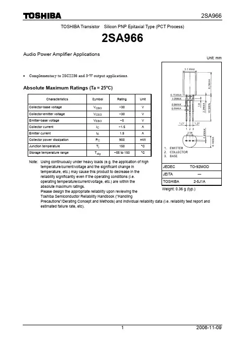
2SD669, 2SD669A
Silicon NPN Epitaxial
Application
Low frequency power amplifier complementary pair with 2SB649/A
Outline
TO-126 MOD
123
1. Emitter 2. Collector 3. Base
1.2 IC = 10 IB
1.0
0.8
0.6
0.4
0.2
0 1 3 10 30 100 300 1,000 Collector current IC (mA)
T
C= –2525
75°C
4
Base to emitter saturation voltage VBE(sat) (V) Collector output capacitance Cob (pF)
V
120
160
V
5
5
V
1.5
1.5A33 NhomakorabeaA
1
1
W
20
20
W
150
150
°C
–55 to +150
–55 to +150
°C
2
2SD669, 2SD669A
Electrical Characteristics (Ta = 25°C)
2SD669
2SD669A
Item
Symbol Min Typ Max Min Typ Max
2. Products and product specifications may be subject to change without notice. Confirm that you have received the latest product standards or specifications before final design, purchase or use.
Collector Output Capacitance vs. Collector to Base Voltage 200 f = 1 MHz 100 IE = 0
50
20 10
5
2 12
5 10 20 50 100
Collector to base voltage VCB (V)
5
元器件交易网
D 160 to 320 —
Collector power dissipation PC (W) Collector current IC (A)
Maximum Collector Dissipation Curve
30
20
10
0
50
100
150
Case temperature TC (°C)
Area of Safe Operation
3
2SD669, 2SD669A
Collector current IC (A)
Typical Output Characteristecs
1.0 0.8 0.6
5.5 5.40.54.0 3.5 3.0 2.5 2.0
TC = 25°C P C = 20 W
1.5 0.4
1.0
0.2
0.5 mA
TO-126 Mod — — 0.67 g
Cautions
1. Hitachi neither warrants nor grants licenses of any rights of Hitachi’s or any third party’s patent, copyright, trademark, or other intellectual property rights for information contained in this document. Hitachi bears no responsibility for problems that may arise with third party’s rights, including intellectual property rights, in connection with use of the information contained in this document.
5
—— 5
——
Collector cutoff current ICBO
— — 10 — — 10
DC current transfer ratio hFE1*1
60 — 320 60 — 200
hFE2
30 — — 30 — —
Collector to emitter saturation voltage
Gain bandwidth product fT (MHz)
Base to Emitter Saturation Voltage vs. Collector Current
1.2 IC = 10 IB
1.0
0.8
TC = –25°C
25
0.6
75
0.4
0.2
0 1 3 10 30 100 300 1,000
50
20 10
5
2 1
0 0.2 0.4 0.6 0.8 1.0 Base to emitter voltage VBE (V)
DC current transfer ratio hFE
DC Current Transfer Ratio vs. Collector Current
300 Ta = 75°C
3. Hitachi makes every attempt to ensure that its products are of high quality and reliability. However, contact Hitachi’s sales office before using the product in an application that demands especially high quality and reliability or where its failure or malfunction may directly threaten human life or cause risk of bodily injury, such as aerospace, aeronautics, nuclear power, combustion control, transportation, traffic, safety equipment or medical equipment for life support.
IC = 500 mA, IB = 50 mA*2 VCE = 5 V, IC = 150 mA*2 VCE = 5 V, IC = 150 mA*2
VCB = 10 V, IE = 0, f = 1 MHz
2SD669 2SD669A
B 60 to 120 60 to 120
C 100 to 200 100 to 200
IB = 0
0
10 20 30 40 50
Collector to emitter voltage VCE (V)
Collector current IC (mA) Ta = 75°C 25 –25
Typical Transfer Characteristics 500 200 VCE = 5 V 100
Collector current IC (mA)
2SD669, 2SD669A
Gain Bandwidth Product
vs. Collector Current
240 VCE = 5 V Ta = 25°C
200
160
120
80
40
0
10
30
100
300
1,000
Collector current IC (mA)
4. Design your application so that the product is used within the ranges guaranteed by Hitachi particularly for maximum rating, operating supply voltage range, heat radiation characteristics, installation conditions and other characteristics. Hitachi bears no responsibility for failure or damage when used beyond the guaranteed ranges. Even within the guaranteed ranges, consider normally foreseeable failure rates or failure modes in semiconductor devices and employ systemic measures such as failsafes, so that the equipment incorporating Hitachi product does not cause bodily injury, fire or other consequential damage due to operation of the Hitachi product.
25 200
150
–25
100
50
VCE = 5 V
1 1 3 10 30 100 300 1,000 3,000
Collector current IC (mA)
Collector to emitter saturation voltage VCE(sat) (V)
Collector to Emitter Saturation Voltage vs. Collector Current
VCE(sat)
——
1
——1
Base to emitter voltage VBE
Gain bandwidth product fT
Collector output
Cob
capacitance
— — 1.5 — — 1.5 — 140 — — 140 — — 14 — — 14 —
Notes: 1. The 2SD669 and 2SD669A are grouped by hFE1 as follows. 2. Pulse test.
2SD669, 2SD669A
Silicon NPN Epitaxial
Application
Low frequency power amplifier complementary pair with 2SB649/A
Outline
TO-126 MOD
123
1. Emitter 2. Collector 3. Base
1.2 IC = 10 IB
1.0
0.8
0.6
0.4
0.2
0 1 3 10 30 100 300 1,000 Collector current IC (mA)
T
C= –2525
75°C
4
Base to emitter saturation voltage VBE(sat) (V) Collector output capacitance Cob (pF)
V
120
160
V
5
5
V
1.5
1.5A33 NhomakorabeaA
1
1
W
20
20
W
150
150
°C
–55 to +150
–55 to +150
°C
2
2SD669, 2SD669A
Electrical Characteristics (Ta = 25°C)
2SD669
2SD669A
Item
Symbol Min Typ Max Min Typ Max
2. Products and product specifications may be subject to change without notice. Confirm that you have received the latest product standards or specifications before final design, purchase or use.
Collector Output Capacitance vs. Collector to Base Voltage 200 f = 1 MHz 100 IE = 0
50
20 10
5
2 12
5 10 20 50 100
Collector to base voltage VCB (V)
5
元器件交易网
D 160 to 320 —
Collector power dissipation PC (W) Collector current IC (A)
Maximum Collector Dissipation Curve
30
20
10
0
50
100
150
Case temperature TC (°C)
Area of Safe Operation
3
2SD669, 2SD669A
Collector current IC (A)
Typical Output Characteristecs
1.0 0.8 0.6
5.5 5.40.54.0 3.5 3.0 2.5 2.0
TC = 25°C P C = 20 W
1.5 0.4
1.0
0.2
0.5 mA
TO-126 Mod — — 0.67 g
Cautions
1. Hitachi neither warrants nor grants licenses of any rights of Hitachi’s or any third party’s patent, copyright, trademark, or other intellectual property rights for information contained in this document. Hitachi bears no responsibility for problems that may arise with third party’s rights, including intellectual property rights, in connection with use of the information contained in this document.
5
—— 5
——
Collector cutoff current ICBO
— — 10 — — 10
DC current transfer ratio hFE1*1
60 — 320 60 — 200
hFE2
30 — — 30 — —
Collector to emitter saturation voltage
Gain bandwidth product fT (MHz)
Base to Emitter Saturation Voltage vs. Collector Current
1.2 IC = 10 IB
1.0
0.8
TC = –25°C
25
0.6
75
0.4
0.2
0 1 3 10 30 100 300 1,000
50
20 10
5
2 1
0 0.2 0.4 0.6 0.8 1.0 Base to emitter voltage VBE (V)
DC current transfer ratio hFE
DC Current Transfer Ratio vs. Collector Current
300 Ta = 75°C
3. Hitachi makes every attempt to ensure that its products are of high quality and reliability. However, contact Hitachi’s sales office before using the product in an application that demands especially high quality and reliability or where its failure or malfunction may directly threaten human life or cause risk of bodily injury, such as aerospace, aeronautics, nuclear power, combustion control, transportation, traffic, safety equipment or medical equipment for life support.
IC = 500 mA, IB = 50 mA*2 VCE = 5 V, IC = 150 mA*2 VCE = 5 V, IC = 150 mA*2
VCB = 10 V, IE = 0, f = 1 MHz
2SD669 2SD669A
B 60 to 120 60 to 120
C 100 to 200 100 to 200
IB = 0
0
10 20 30 40 50
Collector to emitter voltage VCE (V)
Collector current IC (mA) Ta = 75°C 25 –25
Typical Transfer Characteristics 500 200 VCE = 5 V 100
Collector current IC (mA)
2SD669, 2SD669A
Gain Bandwidth Product
vs. Collector Current
240 VCE = 5 V Ta = 25°C
200
160
120
80
40
0
10
30
100
300
1,000
Collector current IC (mA)
4. Design your application so that the product is used within the ranges guaranteed by Hitachi particularly for maximum rating, operating supply voltage range, heat radiation characteristics, installation conditions and other characteristics. Hitachi bears no responsibility for failure or damage when used beyond the guaranteed ranges. Even within the guaranteed ranges, consider normally foreseeable failure rates or failure modes in semiconductor devices and employ systemic measures such as failsafes, so that the equipment incorporating Hitachi product does not cause bodily injury, fire or other consequential damage due to operation of the Hitachi product.