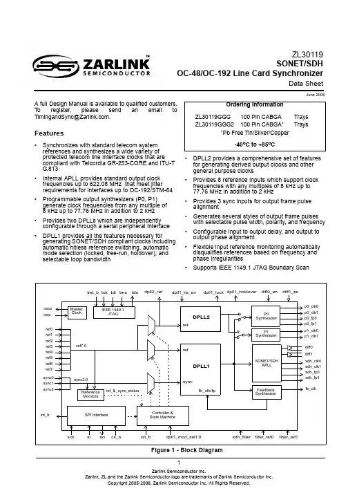
1A full Design Manual is available to qualified customers.To register, please send an email to TimingandSync@.Features•Synchronizes with standard telecom system references and synthesizes a wide variety of protected telecom line interface clocks that are compliant with Telcordia GR-253-CORE and ITU-T G.813•Internal APLL provides standard output clock frequencies up to 622.08MHz that meet jitter requirements for interfaces up to OC-192/STM-64•Programmable output synthesizers (P0, P1) generate clock frequencies from any multiple of 8kHz up to 77.76MHz in addition to 2kHz •Provides two DPLLs which are independently configurable through a serial peripheral interface •DPLL1 provides all the features necessary forgenerating SONET/SDH compliant clocks including automatic hitless reference switching, automatic mode selection (locked, free-run, holdover), and selectable loop bandwidth•DPLL2 provides a comprehensive set of features for generating derived output clocks and other general purpose clocks•Provides 8 reference inputs which support clock frequencies with any multiples of 8kHz up to 77.76MHz in addition to 2kHz•Provides 3 sync inputs for output frame pulse alignment•Generates several styles of output frame pulses with selectable pulse width, polarity, and frequency •Configurable input to output delay, and output to output phase alignment•Flexible input reference monitoring automatically disqualifies references based on frequency and phase irregularities•Supports IEEE 1149.1 JTAG Boundary ScanJune 2006Figure 1 - Block DiagramZL30119 SONET/SDHOC-48/OC-192 Line Card SynchronizerData SheetOrdering InformationZL30119GGG 100 Pin CABGA Trays ZL30119GGG2100 Pin CABGA*Trays*Pb Free Tin/Silver/Copper-40o C to +85o CZL30119Data SheetApplications•AMCs for AdvancedTCA TM and MicroTCA Systems•Multi-Service Edge Switches or Routers•DSLAM Line Cards•WAN Line Cards•RNC/Mobile Switching Center Line Cards•ADM Line CardsZL30119Data SheetTable of Contents1.0 Functional Description . . . . . . . . . . . . . . . . . . . . . . . . . . . . . . . . . . . . . . . . . . . . . . . . . . . . . . . . . . . . . . . . .121.1 DPLL Features . . . . . . . . . . . . . . . . . . . . . . . . . . . . . . . . . . . . . . . . . . . . . . . . . . . . . . . . . . . . . . . . . . . . .121.2 DPLL Mode Control. . . . . . . . . . . . . . . . . . . . . . . . . . . . . . . . . . . . . . . . . . . . . . . . . . . . . . . . . . . . . . . . . .131.3 Ref and Sync Inputs . . . . . . . . . . . . . . . . . . . . . . . . . . . . . . . . . . . . . . . . . . . . . . . . . . . . . . . . . . . . . . . . .141.4 Ref and Sync Monitoring. . . . . . . . . . . . . . . . . . . . . . . . . . . . . . . . . . . . . . . . . . . . . . . . . . . . . . . . . . . . . .151.5 Output Clocks and Frame Pulses . . . . . . . . . . . . . . . . . . . . . . . . . . . . . . . . . . . . . . . . . . . . . . . . . . . . . . .161.6 Configurable Input-to-Output and Output-to-Output Delays . . . . . . . . . . . . . . . . . . . . . . . . . . . . . . . . . . .182.0 Software Configuration. . . . . . . . . . . . . . . . . . . . . . . . . . . . . . . . . . . . . . . . . . . . . . . . . . . . . . . . . . . . . . . . .193.0 References . . . . . . . . . . . . . . . . . . . . . . . . . . . . . . . . . . . . . . . . . . . . . . . . . . . . . . . . . . . . . . . . . . . . . . . . . . .26ZL30119Data SheetList of FiguresFigure 1 - Block Diagram. . . . . . . . . . . . . . . . . . . . . . . . . . . . . . . . . . . . . . . . . . . . . . . . . . . . . . . . . . . . . . . . . . . . . 1 Figure 2 - Automatic Mode State Machine. . . . . . . . . . . . . . . . . . . . . . . . . . . . . . . . . . . . . . . . . . . . . . . . . . . . . . . 13 Figure 3 - Reference and Sync Inputs. . . . . . . . . . . . . . . . . . . . . . . . . . . . . . . . . . . . . . . . . . . . . . . . . . . . . . . . . . 14 Figure 4 - Output Frame Pulse Alignment. . . . . . . . . . . . . . . . . . . . . . . . . . . . . . . . . . . . . . . . . . . . . . . . . . . . . . . 14 Figure 5 - Behaviour of the Guard Soak Timer during CFM or SCM Failures. . . . . . . . . . . . . . . . . . . . . . . . . . . . 16 Figure 6 - Output Clock Configuration. . . . . . . . . . . . . . . . . . . . . . . . . . . . . . . . . . . . . . . . . . . . . . . . . . . . . . . . . . 17 Figure 7 - Phase Delay Adjustments . . . . . . . . . . . . . . . . . . . . . . . . . . . . . . . . . . . . . . . . . . . . . . . . . . . . . . . . . . . 18ZL30119Data SheetList of TablesTable 1 - DPLL1 and DPLL2 Features. . . . . . . . . . . . . . . . . . . . . . . . . . . . . . . . . . . . . . . . . . . . . . . . . . . . . . . . . . 12 Table 2 - Set of Pre-Defined Auto-Detect Clock Frequencies . . . . . . . . . . . . . . . . . . . . . . . . . . . . . . . . . . . . . . . . 15 Table 3 - Set of Pre-Defined Auto-Detect Sync Frequencies. . . . . . . . . . . . . . . . . . . . . . . . . . . . . . . . . . . . . . . . . 15 Table 4 - Output Clock and Frame Pulse Frequencies . . . . . . . . . . . . . . . . . . . . . . . . . . . . . . . . . . . . . . . . . . . . . 17 Table 5 - Register Map. . . . . . . . . . . . . . . . . . . . . . . . . . . . . . . . . . . . . . . . . . . . . . . . . . . . . . . . . . . . . . . . . . . . . . 19ZL30119Data Sheet The following table captures the changes from the December 2005 issue.Page Item Change22-23Software Register Description Changed the naming and description of the framepulse delay offset registers to clearly show thatthey form a 22-bit register spread out over 3 8-bitregisters. The 22-bit register must be considered amulti-byte register during a read or write operation.This affects registers 0x40-0x42, 0x45-0x47, and0x58-0x5A.ZL30119Data Sheet Pin DescriptionPin # Name I/OType DescriptionInput ReferenceC1 B2 A3 C3 B3 B4 C4 A4ref0ref1ref2ref3ref4ref5ref6ref7I d Input References (LVCMOS, Schmitt Trigger). These are input referencesavailable to both DPLL1 and DPLL2 for synchronizing output clocks. All eightinput references can be automatically or manually selected using softwareregisters. These pins are internally pulled down to Vss.B1 A1 A2sync0sync1sync2I d Frame Pulse Synchronization References (LVCMOS, Schmitt Trigger).These are the frame pulse synchronization inputs associated with inputreferences 0, 1 and 2. These inputs accept frame pulses in a clock format (50%duty cycle) or a basic frame pulse format with minimum pulse width of 5 ns.These pins are internally pulled down to V ss.Output Clocks and Frame PulsesD10sdh_clk0O SONET/SDH Output Clock 0 (LVCMOS). This output can be configured toprovide any one of the SONET/SDH clock outputs up to 77.76MHz. The defaultfrequency for this output is 77.76MHz.G10sdh_clk1O SONET/SDH Output Clock 1 (LVCMOS). This output can be configured toprovide any one of the SONET/SDH clock outputs up to 77.76MHz. The defaultfrequency for this output is 19.44MHz.E10sdh_fp0O SONET/SDH Output Frame Pulse 0 (LVCMOS). This output can be configuredto provide virtually any style of output frame pulse synchronized with anassociated SONET/SDH family output clock. The default frequency for this framepulse output is 8kHz.F10sdh_fp1O SONET/SDH Output Frame Pulse 1 (LVCMOS). This output can be configuredto provide virtually any style of output frame pulse synchronized with anassociated SONET/SDH family output clock. The default frequency for this framepulse output is 2kHz.K9p0_clk0O Programmable Synthesizer 0 - Output Clock 0 (LVCMOS). This output can beconfigured to provide any frequency with a multiple of 8kHz up to 77.76MHz inaddition to 2kHz. The default frequency for this output is 2.048MHz.K7p0_clk1O Programmable Synthesizer 0 - Output Clock 1 (LVCMOS). This is aprogrammable clock output configurable as a multiple or division of the p0_clk0frequency within the range of 2 kHz to 77.76 MHz. The default frequency for thisoutput is 8.192MHz.K8p0_fp0O Programmable Synthesizer 0 - Output Frame Pulse 0 (LVCMOS). This outputcan be configured to provide virtually any style of output frame pulse associatedwith the p0 clocks. The default frequency for this frame pulse output is 8kHz.J7p0_fp1O Programmable Synthesizer 0 - Output Frame Pulse 1 (LVCMOS). This outputcan be configured to provide virtually any style of output frame pulse associatedwith the p0 clocks. The default frequency for this frame pulse output is 8kHz.ZL30119Data SheetJ10p1_clk0OProgrammable Synthesizer 1 - Output Clock 0 (LVCMOS). This output can be configured to provide any frequency with a multiple of 8kHz up to 77.76MHz in addition to 2kHz. The default frequency for this output is 1.544MHz (DS1).K10p1_clk1OProgrammable Synthesizer1 - Output Clock 1 (LVCMOS). This is aprogrammable clock output configurable as a multiple or division of the p1_clk0 frequency within the range of 2kHz to 77.76MHz. The default frequency for this output is 3.088MHz (2x DS1).H10fb_clk OFeedback Clock (LVCMOS). This output is a buffered copy of the feedback clock for DPLL1. The frequency of this output always equals the frequency of the selected reference.E1dpll2_ref ODPLL2 Selected Output Reference (LVCMOS). This is a buffered copy of the output of the reference selector for DPLL2. Switching between input reference clocks at this output is not hitless.A9B10diff0_p diff0_n ODifferential Output Clock 0 (LVPECL). This output can be configured to provide any one of the available SDH clocks. The default frequency for this clock output is 155.52MHz.A10B9diff1_p diff1_nODifferential Output Clock 1 (LVPECL). This output can be configured to provide any one of the available SDH clocks. The default frequency for this clock output is 622.08MHz clock.Control H5rst_b IReset (LVCMOS, Schmitt Trigger). A logic low at this input resets the device. To ensure proper operation, the device must be reset after power-up. Reset should be asserted for a minimum of 300ns.J5dpll1_hs_enI uDPLL1 Hitless Switching Enable (LVCMOS, Schmitt Trigger). A logic high at this input enables hitless reference switching. A logic low disables hitless reference switching and re-aligns DPLL1’s output phase to the phase of the selected reference input. This feature can also be controlled through software registers. This pin is internally pull up to Vdd.C2D2dpll1_mod_sel0dpll1_mod_sel1I uDPLL1 Mode Select 1:0 (LVCMOS, Schmitt Trigger). During reset, the levels on these pins determine the default mode of operation for DPLL1 (Automatic, Normal, Holdover or Freerun). After reset, the mode of operation can becontrolled directly with these pins, or by accessing the dpll1_modesel register through the serial interface. This pin is internally pull up to Vdd.K1diff0_enI uDifferential Output 0 Enable (LVCMOS, Schmitt Trigger). When set high, the differential LVPECL output 0 driver is enabled. When set low, the differential driver is tristated reducing power consumption. This pin is internally pull up to Vdd.D3diff1_enI uDifferential Output 1 Enable (LVCMOS, Schmitt Trigger). When set high, the differential LVPECL output 1 driver is enabled. When set low, the differential driver is tristated reducing power consumption.This pin is internally pull up to Vdd.Pin # Name I/O Type DescriptionZL30119Data SheetStatus H1dpll1_lockOLock Indicator (LVCMOS). This is the lock indicator pin for DPLL1. This output goes high when DPLL1’s output is frequency and phase locked to the input reference.J1dpll1_holdover OHoldover Indicator (LVCMOS). This pin goes high when DPLL1 enters the holdover mode.Serial Interface E2sck I Clock for Serial Interface (LVCMOS). Serial interface clock.F1si I Serial Interface Input (LVCMOS). Serial interface data input pin.G1so O Serial Interface Output (LVCMOS). Serial interface data output pin.E3cs_b I u Chip Select for Serial Interface (LVCMOS). Serial interface chip select. This pin is internally pull up to Vdd.G2int_bOInterrupt Pin (LVCMOS). Indicates a change of device status prompting the processor to read the enabled interrupt service registers (ISR). This pin is an open drain, active low and requires an external pull up to VDD.APLL Loop Filter A6sdh_filter A External Analog PLL Loop Filter terminal.B6filter_ref0A Analog PLL External Loop Filter Reference.C6filter_ref1AAnalog PLL External Loop Filter Reference.JTAG and Test J4tdoOTest Serial Data Out (Output). JTAG serial data is output on this pin on the falling edge of tck. This pin is held in high impedance state when JTAG scan is not enabled.K2tdiI uTest Serial Data In (Input). JTAG serial test instructions and data are shifted in on this pin. This pin is internally pull up to Vdd. If this pin is not used then it should be left unconnected.H4trst_bI uTest Reset (LVCMOS). Asynchronously initializes the JTAG TAP controller by putting it in the Test-Logic-Reset state. This pin should be pulsed low on power-up to ensure that the device is in the normal functional state. This pin is internally pulled up to Vdd. If this pin is not used then it should be connected to GND.K3tck I Test Clock (LVCMOS): Provides the clock to the JTAG test logic. If this pin is not used then it should be pulled down to GND.J3tmsI uTest Mode Select (LVCMOS). JTAG signal that controls the state transitions of the TAP controller. This pin is internally pulled up to V DD . If this pin is not used then it should be left unconnected.Pin # NameI/O TypeDescriptionZL30119Data SheetMaster ClockK4osci I Oscillator Master Clock Input (LVCMOS). This input accepts a 20MHzreference from a clock oscillator (TCXO, OCXO). The stability and accuracy ofthe clock at this input determines the free-run accuracy and the long termholdover stability of the output clocks.K5osco O Oscillator Master Clock Output (LVCMOS). This pin must be left unconnectedwhen the osci pin is connected to a clock oscillator.MiscellaneousB5C5G3NC No Connection. Leave unconnected.J2J6H7IC Internal Connection. Connect to ground.D1K6F2F3IC Internal Connection. Leave unconnected.Power and GroundD9 E4 G8 G9 J8 J9 H6 H8V DD PPPPPPPPPositive Supply Voltage. +3.3V DC nominal.E8 F4V CORE PPPositive Supply Voltage. +1.8V DC nominal.A5 A8 C10AV DD PPPPositive Analog Supply Voltage. +3.3V DC nominal.B7 B8 H2AV CORE PPPPositive Analog Supply Voltage. +1.8V DC nominal.Pin # Name I/OType DescriptionZL30119Data SheetI - InputI d -Input, Internally pulled down I u -Input, Internally pulled up O -Output A -Analog P -Power G -GroundD4D5D6D7E5E6E7F5F6F7G4G5G6G7E9F8F9H9V SSG G G G G G G G G G G G G G G G G G Ground. 0 Volts.A7C7C8C9D8H3AV SSG G G G G GAnalog Ground. 0 Volts.Pin # Name I/O Type DescriptionZL30119Data Sheet1.0 Functional DescriptionThe ZL30119 SONET/SDH Line Card Synchronizer is a highly integrated device that provides timing and synchronization for network interface cards. It incorporates two independent DPLLs, each capable of locking to one of eight input references and provides a wide variety of synchronized output clocks and frame pulses.1.1 DPLL FeaturesThe ZL30119 provides two independently controlled Digital Phase-Locked Loops (DPLL1, DPLL2) for clock and/or frame pulse synchronization. Table 1 lists the feature summary for both DPLLs.FeatureDPLL1DPLL2Modes of Operation Free-run, Normal (locked), Holdover Free-run, Normal (locked), Holdover.Loop Bandwidth User selectable: 14Hz, 28Hz, or wideband 1 (890Hz / 56Hz / 14Hz)1. In the wideband mode, the loop bandwidth depends on the frequency of the reference input. For reference frequencies equal to or greater than 64kHz, the loop bandwidth = 890 Hz. For reference frequencies equal to or greater than 8kHz and less than 64 kHz, the loop bandwidth = 56 Hz. For reference frequencies equal to 2kHz, the loop bandwidth is equal to 14Hz.Fixed: 14HzPhase Slope Limiting User selectable: 885ns/s, 7.5µs/s, 61µs/s, or unlimited User selectable: 61µs/s, or unlimited Pull-in Range Fixed: 130ppm Fixed: 130ppm Reference Inputs Ref0 to Ref7Ref0 to Ref7Sync InputsSync0, Sync1, Sync2Sync inputs are not supported.Input Ref Frequencies 2kHz, N * 8kHz up to 77.76 MHz 2kHz, N * 8kHz up to 77.76 MHz Supported Sync Input Frequencies 166.67Hz, 400Hz, 1kHz, 2kHz, 8kHz, 64kHz.Sync inputs are not supported.Input Reference Selection/Switching Automatic (based on programmable priority and revertiveness), or manual Automatic (based on programmable priority and revertiveness), or manual Hitless Ref Switching Can be enabled or disabledCan be enabled or disabled Output Clocksdiff0_p/n, diff1_p/n, sdh_clk0, sdh_clk1, p0_clk0, p0_clk1, p1_clk0, p1_clk1, fb_clk.p0_clk0, p0_clk1, p1_clk0, p1_clk1.Output Frame Pulses sdh_fp0, sdh_fp1, p0_fp0, p0_fp1 synchronized to active sync reference.p0_fp0, p0_fp1 not aligned to sync reference.Supported Output Clock Frequencies As listed in Table 4As listed in Table 4 for p0_clk0, p0_clk1, p1_clk0, p1_clk1Supported Output Frame Pulse Frequencies As listed in Table 4As listed in Table 4 for p0_fp0, p0_fp not aligned to sync reference.External Pins Status IndicatorsLock, HoldoverNoneTable 1 - DPLL1 and DPLL2 FeaturesZL30119Data Sheet1.2 DPLL Mode ControlBoth DPLL1 and DPLL2 independently support three modes of operation - free-run, normal and holdover. The mode of operation can be manually set or controlled by an automatic state machine as shown in Figure 2.Figure 2 - Automatic Mode State MachineFree-runThe free-run mode occurs immediately after a reset cycle or when the DPLL has never been synchronized to areference input. In this mode, the frequency accuracy of the output clocks is equal to the frequency accuracy of the external master oscillator. Lock AcquisitionThe input references are continuously monitored for frequency accuracy and phase regularity. If at least one of the input references is qualified by the reference monitors, then the DPLL will begin lock acquisition on that input. Given a stable reference input, the ZL30119 will enter in the Normal (locked) mode.Normal (locked)The usual mode of operation for the DPLL is the normal mode where the DPLL phase locks to a selected qualified reference input and generates output clocks and frame pulses with a frequency accuracy equal to the frequency accuracy of the reference input. While in the normal mode, the DPLL’s clock and frame pulse outputs comply with the MTIE and TDEV wander generation specifications as described in Telcordia and ITU-T telecommunication standards.HoldoverWhen the DPLL operating in the normal mode loses its reference input, and no other qualified references are available, it will enter the holdover mode and continue to generate output clocks based on historical frequency data collected while the DPLL was synchronized.ResetAnother reference is qualified and availablefor selectionPhase lock on the selected reference is achievedLock AcquisitionNormal (Locked)No references are qualified and available for selectionFree-RunHoldoverSelected referencefailsAll references are monitored for frequency accuracy and phase regularity, and at least one reference is qualified.Normal (Locked)ZL30119Data Sheet1.3 Ref and Sync InputsThere are eight reference clock inputs (ref0 to ref7) available to both DPLL1 and DPLL2. The selected reference input is used to synchronize the output clocks. Each of the DPLLs have independent reference selectors which can be controlled using a built-in state machine or set in a manual mode.Figure 3 - Reference and Sync InputsIn addition to the reference inputs, DPLL1 has three optional frame pulse synchronization inputs (sync0 to sync2)used to align the output frame pulses. The sync n input is selected with its corresponding ref n input, where n = 0, 1,or 2. Note that the sync input cannot be used to synchronize the DPLL, it only determines the alignment of the frame pulse outputs. An example of output frame pulse alignment is shown in Figure 4.Figure 4 - Output Frame Pulse Alignmentref7:0sync2:0DPLL2DPLL1ref nsdh/p0/p1_clk xsdh/p0_fp xWithout a frame pulse signal at the sync input, the output frame pulses will align to any arbitrary cycle of its associated output clock.sync n - no frame pulse signal presentWhen a frame pulse signal is present at the sync input, the DPLL will align the output frame pulses to the output clock edge that is aligned to the input frame pulse.ref n sdh/p0/p1_clk xsdh/p0_fp xsync nn = 0, 1, 2x = 0, 1n = 0, 1, 2x = 0, 1ZL30119Data Sheet Each of the ref inputs accept a single-ended LVCMOS clock with a frequency ranging from 2kHz to 77.76MHz. Built-in frequency detection circuitry automatically determines the frequency of the reference if its frequency is within the set of pre-defined frequencies as shown in Table 2. Custom frequencies definable in multiples of 8kHz are also available.2 kHz8 kHz64 kHz1.544 MHz2.048 MHz6.48 MHz8.192 MHz16.384 MHz19.44 MHz38.88 MHz77.76 MHzCustom ACustom BTable 2 - Set of Pre-Defined Auto-Detect Clock FrequenciesEach of the sync inputs accept a single-ended LVCMOS frame pulse. Since alignment is determined from the rising edge of the frame pulse, there is no duty cycle restriction on this input, but there is a minimum pulse width requirement of 5 ns. Frequency detection for the sync inputs is automatic for the supported frame pulse frequencies shown in Table 3.166.67 Hz(48x 125 µs frames)400 Hz1 kHz2 kHz8 kHz64 kHzTable 3 - Set of Pre-Defined Auto-Detect Sync Frequencies1.4 Ref and Sync MonitoringAll input references (ref0 to ref7) are monitored for frequency accuracy and phase regularity. New references are qualified before they can be selected as a synchronization source, and qualified references are continuously monitored to ensure that they are suitable for synchronization. The process of qualifying a reference depends on four levels of monitoring.Single Cycle Monitor (SCM)The SCM block measures the period of each reference clock cycle to detect phase irregularities or a missing clock edge. In general, if the measured period deviates by more than 50% from the nominal period, then an SCM failure (scm_fail) is declared.ZL30119Data SheetCoarse Frequency Monitor (CFM)The CFM block monitors the reference frequency over a measurement period of 30 µs so that it can quickly detect large changes in frequency. A CFM failure (cfm_fail) is triggered when the frequency has changed by more than 3%or approximately 30000ppm.Precise Frequency Monitor (PFM)The PFM block measures the frequency accuracy of the reference over a 10 second interval. To ensure an accurate frequency measurement, the PFM measurement interval is re-initiated if phase or frequency irregularities are detected by the SCM or CFM. The PFM provides a level of hysteresis between the acceptance range and the rejection range to prevent a failure indication from toggling between valid and invalid for references that are on the edge of the acceptance range.When determining the frequency accuracy of the reference input, the PFM uses the external oscillator’s output frequency (f ocsi ) as its point of reference. Guard Soak Timer (GST)The GST block mimics the operation of an analog integrator by accumulating failure events from the CFM and the SCM blocks and applying a selectable rate of decay when no failures are detected.As shown in Figure 5, a GST failure (gst_fail) is triggered when the accumulated failures have reached the upper threshold during the disqualification observation window. When there are no CFM or SCM failures, the accumulator decrements until it reaches its lower threshold during the qualification window.Figure 5 - Behaviour of the Guard Soak Timer during CFM or SCM FailuresAll sync inputs (sync0 to sync2) are continuously monitored to ensure that there is a correct number of reference clock cycles within the frame pulse period.1.5 Output Clocks and Frame PulsesThe ZL30119 offers a wide variety of outputs including two low-jitter differential LVPECL clocks (diff0_p/n,diff1_p/n ), two SONET/SDH LVCMOS (sdh_clk0, sdh_clk1) output clocks and four programmable LVCMOS (p0_clk0, p0_clk1, p1_clk0, p1_clk1) output clocks. In addition to the clock outputs, two LVCMOS SONET/SDH frame pulse outputs (sdh_fp0, sdh_fp1) and two LVCMOS programmable frame pulses (p0_fp0, p0_fp1) are also available.refCFM or SCM failuresupper thresholdlower thresholdt d - disqualification timet q - qualification time = n * t dt dt qgst_failZL30119Data SheetThe feedback clock (fb_clk ) of DPLL1 is available as an output clock. Its output frequency is always equal to DPLL1’s selected input frequency.The output clocks and frame pulses derived from the SONET/SDH APLL are always synchronous with DPLL1, and the clocks and frame pulses generated from the programmable synthesizers can be synchronized to either DPLL1or DPLL2. This allows the ZL30119 to have two independent timing paths.Figure 6 - Output Clock ConfigurationThe supported frequencies for the output clocks and frame pulses are shown in Table 4.diff0_p/n, diff1_p/n (LVPECL)sdh_clk0, sdh_clk1(LVCMOS)p0_clk0, p1_clk0(LVCMOS)p0_clk1, p1_clk1(LVCMOS)sdh_fp0, shd_fp1, p0_fp0, p0_fp1(LVCMOS)6.48 MHz 6.48 MHz 2 kHz p x _clk0 p x _clk1 =2M166.67 Hz (48x 125 µs frames)19.44 MHz 9.72 MHz N * 8 kHz (up to 77.76 MHz)400 Hz 38.88 MHz 12.96 MHz 1 kHz 51.84 MHz 19.44 MHz 2 kHz 77.76 MHz 25.92 MHz 4 kHz 155.52 MHz 38.88 MHz 8 kHz 311.04 MHz 51.84 MHz 32 kHz 622.08 MHz77.76 MHz64 kHzTable 4 - Output Clock and Frame Pulse FrequenciesDPLL2p0_clk0p0_fp0p0_clk1p0_fp1 P0 SynthesizerDPLL1p1_clk0p1_clk1P1 Synthesizersdh_clk0sdh_fp0sdh_clk1sdh_fp1SONET/SDHAPLLdiff0diff1Feedback Synthesizerfb_clkZL30119Data Sheet1.6 Configurable Input-to-Output and Output-to-Output DelaysThe ZL30119 allows programmable static delay compensation for controlling input-to-output and output-to-output delays of its clocks and frame pulses.All of the output synthesizers (SONET/SDH, P0, P1, Feedback) locked to DPLL1 can be configured to lead or lag the selected input reference clock using the DPLL1 Fine Delay . The delay is programmed in steps of 119.2ps with a range of -128 to +127 steps giving a total delay adjustment in the range of -15.26ns to +15.14ns. Negative values delay the output clock, positive values advance the output clock. Synthesizers that are locked to DPLL2 are unaffected by this delay adjustment.In addition to the fine delay introduced in the DPLL1 path, the SONET/SDH, P0, and P1 synthesizers have the ability to add their own fine delay adjustments using the P0 Fine Delay , P1 Fine Delay , and SDH Fine Delay .These delays are also programmable in steps of 119.2ps with a range of -128 to +127 steps.In addition to these delays, the single-ended output clocks of the SONET/SDH, P0, and P1 synthesizers can be independently offset by 90, 180 and 270 degrees using the Coarse Delay , and the SONET/SDH differential outputs can be independently delayed by -1.6ns, 0ns, +1.6ns or +3.2ns using the Diff Delay . The output frame pulses (SONET/SDH, P0) can be independently offset with respect to each other using the FP Delay .Figure 7 - Phase Delay AdjustmentsDPLL1DPLL2P0 Fine Delayp0_clk0p0_clk1p0_fp0p0_fp1 P0 SynthesizerCoarse DelayCoarse Delay FP Delay FP Delay fb_clkp1_clk0p1_clk1 P1 Fine DelayDiff Delay Diff Delaydiff0diff1 SONET/SDHAPLLsdh_clk0sdh_clk1sdh_fp0sdh_fp1 SDH Fine DelayFeedback SynthesizerDPLL1 Fine DelayCoarse Delay Coarse Delay FP Delay FP DelayCoarse Delay Coarse DelayP1 Synthesizer。