
宏基笔记本原理图(acer电路图)
- 格式:pdf
- 大小:850.77 KB
- 文档页数:26
A p p e n d i x DSchematics
This appendix shows the schematic diagrams of the notebook. 电子发烧友 电子技术论坛
Date: February 12, 1997Sheet 1of 25SizeDocument NumberREV
A396149SCTitle
370P/J (CPU)TAIPEI TAIWAN R.O.CACER 1
2
3
4
5678910RP19
SRP10K
$CACHE#$HLOCK#
$AP
$BUSCHK#$FRCMC#
$FLUSH#$WBWT#
$PEN#3.3V
3.3V1
2R214
10KR3
$DC#$MIO#$WR#
$CPURST
$SMIACT#$CPUADS#
$CPUSMI#$TCK$WBWT#
$TRST#2.9V
3.3V
##
222
4
22,5
8R214 NOT INSTALLA3-AL35258
A4-AM34294
A5-AK32255
A6-AN33293
A7-AL33256
A8-AM32292
A9-AK30253
A10-AN31291
A11-AL31254
A12-AL29252
A13-AK28251
A14-AL27250
A15-AK26249
A16-AL25248
A17-AK24247
A18-AL23246
A19-AK22245
A20-AL21244
A21-AF34204
A22-AH36216
A23-AE33203
A24-AG35215
A25-AJ35222
A26-AH34214
A27-AG33213
A28-AK36259
A29-AK34257
A30-AM36296
A31-AJ33221
A20M#-AK8231
AHOLD-V4151
AP-AK2225BE0#-AL9232
BE1#-AK10233
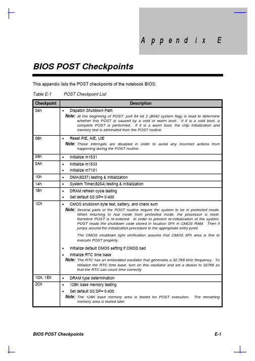
A p A p p e n d p e n d i x E i x EBIOS POST CheckpointsBIOS POST CheckpointsE-1This appendix lists the POST checkpoints of the notebook BIOS.Table E-1POST Checkpoint ListCheckpointDescription04h• Dispatch Shutdown PathNote:At the beginning of POST, port 64 bit 2 (8042 system flag) is read to determinewhether this POST is caused by a cold or warm boot. If it is a cold boot, acomplete POST is performed. If it is a warm boot, the chip initialization andmemory test is eliminated from the POST routine.08h• Reset PIE, AIE, UIENote:These interrupts are disabled in order to avoid any incorrect actions fromhappening during the POST routine.09h• Initialize m15310Ah• Initialize m1533• Initialize m710110h• DMA(8237) testing & initialization14h• System Timer(8254) testing & initialization18h• DRAM refresh cycle testing• Set default SS:SP= 0:4001Ch• CMOS shutdown byte test, battery, and check sumNote:Several parts of the POST routine require the system to be in protected mode.When returning to real mode from protected mode, the processor is reset,therefore POST is re-entered. In order to prevent re-initialization of the system,POST reads the shutdown code stored in location 0Fh in CMOS RAM. Then itjumps around the initialization procedure to the appropriate entry point.The CMOS shutdown byte verification assures that CMOS 0Fh area is fine toexecute POST properly.• Initialize default CMOS setting if CMOS bad• Initialize RTC time baseNote:The RTC has an embedded oscillator that generates a 32.768 KHz frequency. Toinitialize the RTC time base, turn on this oscillator and set a divisor to 32768 sothat the RTC can count time correctly1Dh, 1Eh• DRAM type determination2Ch• 128K base memory testing• Set default SS:SP= 0:400Note:The 128K base memory area is tested for POST execution. The remainingmemory area is tested later.
器材:ZTE-T U880
器材:ZTE-T U880
器材:ZTE-T U880
器材:ZTE-T U880
器材:ZTE-T U880
器材:ZTE-T U880
器材:ZTE-T U880
器材:ZTE-T U880
器材:ZTE-T U880
器材:ZTE-T U880
器材:ZTE-T U880
器材:ZTE-T U880
器材:ZTE-T U880
器材:ZTE-T U880
器材:ZTE-T U880
器材:ZTE-T U880
器材:ZTE-T U880
器材:ZTE-T U880
器材:ZTE-T U880
器材:ZTE-T U880
器材:ZTE-T U880
器材:ZTE-T U880
器材:ZTE-T U880
器材:ZTE-T U880
器材:ZTE-T U880
器材:ZTE-T U880
器材:ZTE-T U880
器材:ZTE-T U880
器材:ZTE-T U880
器材:ZTE-T U880
器材:ZTE-T U880
器材:ZTE-T U880
器材:ZTE-T U880
器材:ZTE-T U880
器材:ZTE-T U880

宏基(acer)Aspire4930G拆机教程
宏基(acer)Aspire 4930G拆机教程
电脑是宏基Aspire4930G系列的(具体型号是731G16Mn),鲁大师经常对CPU温度报警。
1.拆机前的样子
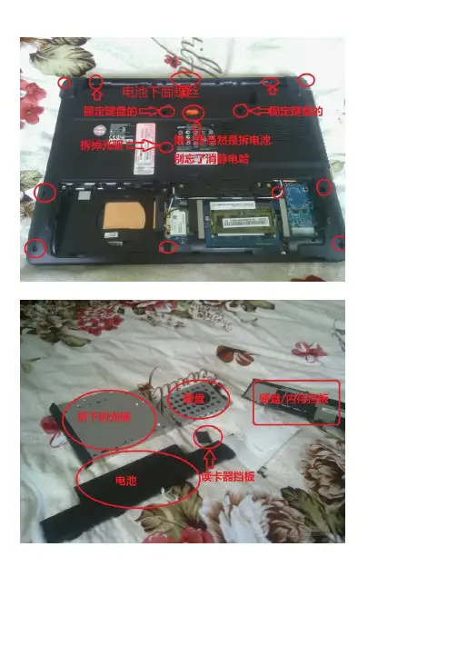
2.按照图中画圆圈标定的螺丝位置先拆下背面的所有螺丝和保护盖(注:背面一共6个较小的螺丝,13个较大的螺丝其中有几个是固定保护盖的,在这里没有画出) 3.拆下硬盘和无线网卡(无线网卡上有两个固定的螺丝必须先拆下,并且一黑一白两根导线要轻轻地从上面摘下,这两根导线连接着屏幕)
4.拆下键盘
先找到键盘上两个卡扣,用小螺丝刀将卡扣压进卡槽,轻轻向上搬动最上排的按键就可以轻松地把键盘拆下
但是不要太用力,因为键盘下边连着排线,如果用力太大会将排线扯坏,从此步之后会经常遇到排线拆卸。拆卸排线时只要两手分别用一个螺丝刀同时轻轻地将压住排线的卡扣向外搬动,然后将排线向外轻轻抽出就可以了,以后对于的处理方法也一样。
接下来将标记处的排线都拆下
5.拆下靠近屏幕的开机键以及多媒体键区域
由于背面的螺丝已经全部拆除,所以现在这个区域已经没有螺丝固定所以只要沿着这个区域的外延用小螺丝刀轻轻撬动就可以轻松的将其拆下,不过值得注意的是这个键区仍有一个排线,应用上面介绍的方法就可以将其拆下
6。卸下面板上的螺丝并拆掉屏幕排线。(此处有8个较小螺丝2个较大螺丝图中指标出三个较小的螺丝,其余的螺丝都在刚刚拆下的多媒体键面板下方,其中有两个较大螺丝和两个较小螺丝是固定屏幕的,将这四个螺丝拆下之后要小心扶住屏幕防止屏幕摔坏)
屏幕排线(黄色圆圈) 7.卸下屏幕同时拔出无线网卡连在屏幕上的两根导线(无线网卡连接到屏幕有两根天线,也就是前面提到的那一黑一白两根导线,由于这样根导线会妨碍以后的操作,必须现在抽出,这两根导线从机器的下底壳穿到上面板线路比较复杂所以要记清楚走线的方式。
背面的线路