LM3S3748开发板原理图
- 格式:pdf
- 大小:100.07 KB
- 文档页数:5
Stellaris® LM3S9B96 Development Kit User’s ManualCopyrightCopyright © 2009 Texas Instruments, Inc. All rights reserved. Stellaris and StellarisWare are registered trademarks of Texas Instruments. ARM and Thumb are registered trademarks, and Cortex is a trademark of ARM Limited. Other names and brands may be claimed as the property of others. Texas Instruments108 Wild Basin, Suite 350Austin, TX 78746Main: +1-512-279-8800Fax: +1-512-279-8879Stellaris® LM3S9B96 Development Kit User’s ManualTable of ContentsChapter 1: Stellaris® LM3S9B96 Development Board Overview (7)Features (7)Development Kit Contents (10)Block Diagram (11)Development Board Specifications (11)Chapter 2: Stellaris® LM3S9B96 Development Board Hardware Description (13)LM3S9B96 Microcontroller Overview (13)Jumpers and GPIO Assignments (13)Clocking (14)Reset (15)Power Supplies (15)USB (15)Debugging (16)Color QVGA LCD Touch Panel (17)I2S Audio (19)User Switch and LED (19)Chapter 3: Stellaris® LM3S9B96 Development Board External Peripheral Interface (EPI) (21)SDRAM Expansion Board (21)Flash and SRAM Memory Expansion Board (21)Chapter 4: Using the In-Circuit Debugger Interface (23)Appendix A: Stellaris® LM3S9B96 Development Board Schematics (25)Appendix B: Stellaris® LM3S9B96 Development Board Component Locations (33)Appendix C: Stellaris® LM3S9B96 Development Board Connection Details (35)DC Power Jack (35)ARM Target Pinout (35)Appendix D: Stellaris® LM3S9B96 Development Board Microcontroller GPIO Assignments (37)Appendix E: Stellaris® LM3S9B96 Flash and SRAM Memory Expansion Board (41)Installation (41)Features (42)Hardware Description (43)Functional Description (43)Memory Map (45)Component Locations (46)Schematics (46)Appendix F: References (49)List of FiguresFigure1-1.DK-LM3S9B96 Development Board (9)Figure1-2.DK-LM3S9B96 Development Board Block Diagram (11)Figure2-1.Factory Default Jumper Settings (14)Figure4-1.ICD Interface Mode (23)Figure ponent Placement Plot for Top (34)Figure E-1.DK-LM3S9B96-EXP-FS8 Board Image (41)Figure E-2.DK-LM3S9B96 Development Board (42)Figure E-3.DK-LM3S9B96-EXP-FS8 Flash/SRAM/LCD IF Expansion Board Block Diagram (43)Figure ponent Placement Plot for Top and Bottom (46)Stellaris® LM3S9B96 Development Kit User’s ManualList of TablesTable2-1.Board Features and Peripherals that are Disconnected in Factory Default Configuration (13)B-Related Signals (15)Table2-3.Hardware Debugging Configurations (16)Table2-4.Debug-Related Signals (17)Table2-5.LCD-Related Signals (18)Table2-6.I2S Audio-Related Signals (19)Table2-7.Navigation Switch-Related Signals (19)Table C-1.Debug Interface Pin Assignments (35)Table D-1.Microcontroller GPIO Assignments (37)Table E-1.Flash and SRAM Memory Expansion Board Memory Map (45)Table E-2.LCD Latch Register (45)C H A P T E R1Stellaris® LM3S9B96 Development Board Overview The Stellaris® LM3S9B96 Development Board provides a platform for developing systems aroundthe advanced capabilities of the LM3S9B96 ARM® Cortex™-M3-based microcontroller.The LM3S9B96 is a member of the Stellaris Tempest-class microcontroller family. Tempest-classdevices include capabilities such as 80MHz clock speeds, an External Peripheral Interface (EPI)and Audio I2S interfaces. In addition to new hardware to support these features, theDK-LM3S9B96 board includes a rich set of peripherals found on other Stellaris boards.The development board includes an on-board in-circuit debug interface (ICDI) that supports bothJTAG and SWD debugging. A standard ARM 20-pin debug header supports an array of debuggingsolutions.The Stellaris® LM3S9B96 Development Kit accelerates development of Tempest-classmicrocontrollers. The kit also includes extensive example applications and complete source code. FeaturesThe Stellaris® LM3S9B96 Development Board includes the following features.Simple set-up—USB cable provides debugging, communication, and powerFlexible development platform with a wide range of peripheralsColor LCD graphics display–TFT LCD module with 320 x 240 resolution–Resistive touch interface80 MHz LM3S9B96 microcontroller with 256 K Flash, 96 K SRAM, and integrated EthernetMAC+PHY, USB OTG, and CAN communications–– 8 MB SDRAM (plug-in EPI option board)–– EPI break-out board (plug-in option board)1MB serial Flash memoryPrecision 3.00V voltage referenceSAFE RTOS™ operating system in microcontroller ROMI2S stereo audio codec–Line In/Out–Headphone Out–Microphone InController Area Network (CAN) Interface10/100 BaseT EthernetUSB On-The-Go (OTG) Connector–Device, Host, and OTG modesUser LED and push buttonThumbwheel potentiometer (can be used for menu navigation)MicroSD card slotSupports a range of debugging options–Integrated In-circuit Debug Interface (ICDI)–JTAG, SWD, and SWO all supported–Standard ARM® 20-pin JTAG debug connectorUSB Virtual COM PortJumper shunts to conveniently reallocate I/O resourcesDevelop using tools supporting the DK-LM3S9B96 from Keil, IAR, Code Sourcery, and Code RedSupported by StellarisWare® software including the graphics library, the USB library, and the peripheral driver libraryAn optional Flash and SRAM memory expansion board (DK-LM3S9B96-EXP-FS8) is also available for use with the DK-LM3S9B96 development board–Works with the External Peripheral Interface (EPI) of the Stellaris microcontroller–Provides Flash memory, SRAM, and an improved performance LCD interfaceFor more information on the DK-LM3S9B96-EXP-FS8 memory expansion board, seeAppendix E, “Stellaris® LM3S9B96 Flash and SRAM Memory Expansion Board,” on page 41.The DK-LM3S9B96-EXP-FS8 memory expansion board is available for purchase separately.Stellaris® LM3S9B96 Development Kit User’s Manual Figure1-1.DK-LM3S9B96 Development BoardAudio Line Output1MB Serial Flash Memory3.5" LCD Touch PanelDevelopment Kit ContentsThe Stellaris® LM3S9B96 Development Kit contains everything needed to develop and run arange of applications using Stellaris microcontrollers:LM3S9B96 development board8MB SDRAM expansion boardEPI signal breakout boardRetractable Ethernet cableUSB Mini-B cable for debugger useUSB Micro-B cable for OTG-to-PC connectionUSB Micro-A to USB A adapter for USB HostUSB Flash memory stickmicroSD Card20-position ribbon cableCDs containing evaluation versions of the following tools:–StellarisWare with example code for this board–ARM RealView® Microcontroller Development Kit (MDK)–IAR Embedded Workbench® Kickstart Edition–Code Red Technologies Red Suite™–CodeSourcery Sourcery G++™ GNU tools.Stellaris® LM3S9B96 Development Kit User’s Manual Block DiagramFigure1-2.DK-LM3S9B96 Development Board Block DiagramDevelopment Board SpecificationsBoard supply voltage: 4.75–5.25 Vdc from one of the following sources:–Debugger (ICDI) USB cable (connected to a PC)–USB Micro-B cable (connected to a PC)–DC power jack (2.1x5.5mm from external power supply)Break-out power output: 3.3 Vdc (100 mA max)Dimensions (excluding LCD panel):– 4.50” x 4.25” x 0.60” (LxWxH) with SDRAM board– 4.50” x 4.25” x 0.75” (LxWxH) with EPI breakout boardAnalog Reference: 3.0V +/-0.2%RoHS status: CompliantNOTE:When the LM3S9B96 Development Board is used in USB Host mode, the host connector is capable of supplying power to the connected USB device. The available supply current is limited to ~200mA unless the development board is powered from an external 5Vsupply with a =600mA rating.C H A P T E R2Stellaris® LM3S9B96 Development Board Hardware DescriptionIn addition to an LM3S9B96 microcontroller, the development board includes a range of usefulperipheral features and an integrated in-circuit debug interface (ICDI). This chapter describes howthese peripherals operate and interface to the microcontrollerLM3S9B96 Microcontroller OverviewThe Stellaris LM3S9B96 is an ARM Cortex-M3-based microcontroller with 256-KB flash memory,80-MHz operation, Ethernet, USB, EPI, SAFE RTOS™ in ROM, and a wide range of peripherals.See the LM3S9B96 Microcontroller Data Sheet (order number DS-LM3S9B96) for completemicrocontroller details.The LM3S9B96 microcontroller is factory-programmed with a quickstart demo program. Thequickstart program resides in on-chip flash memory and runs each time power is applied, unlessthe quickstart has been replaced with a user program.Jumpers and GPIO AssignmentsEach peripheral circuit on the development board is interfaced to the LM3S9B96 microcontrollerthrough a 0.1” pitch jumper/shunt. Figure2-1 on page 14 shows the factory default positions of thejumpers. The jumpers must be in these positions for the quickstart demo program to functioncorrectly.The development board offers capabilities that the LM3S9B96 cannot support simultaneously dueto pin count and GPIO multiplexing limitations. For example, as configured, the board does notsupport SDRAM and I2S receive (microphone or line input) functions at the same time. Thejumpers associated with I2S receive are omitted in the default configuration.Table2-1 lists all features and peripherals that are disconnected in the factory defaultconfiguration. Using these peripherals requires that other peripherals be disconnected.Appendix D, “Stellaris® LM3S9B96 Development Board Microcontroller GPIO Assignments,” onpage 37 lists alternative jumper configurations used in conjunction with some of theStellarisWare™ example applications for this board.Table2-1.Board Features and Peripherals that are Disconnected in Factory DefaultConfigurationPeripheral JumpersI2S Receive (Audio Input)JP44, 45, 47, 49Controller Area Network (CAN) JP14, 15Ethernet Yellow Status LED (LED2)JP2Analog 3.0V Reference JP33See Appendix D, “Stellaris® LM3S9B96 Development Board Microcontroller GPIO Assignments,”on page 37, for a complete list of GPIO assignments. The table lists all default and alternateassignments that are supported by the 0.1”jumpers and PCB routing. The LM3S9B96 hasadditional internal multiplexing that enables additional configurations which may require discretewiring between peripherals and GPIO pins.The ICDI section of the board has a GND-GND jumper that serves no function other than toprovide a convenient place to ‘park’ a spare jumper. This jumper may be reused as required.ClockingThe development board uses a 16.0-MHz (Y2) crystal to complete the LM3S9B96microcontroller's main internal clock circuit. An internal PLL, configured in software, multiples thisclock to higher frequencies for core and peripheral timing.A 25.0-MHz (Y1) crystal provides an accurate timebase for the Ethernet PHY.Stellaris® LM3S9B96 Development Kit User’s ManualResetThe RESETn signal into the LM3S9B96 microcontroller connects to the reset switch (SW2) and tothe ICDI circuit for a debugger-controlled reset.External reset is asserted (active low) under any one of the three following conditions:Power-on reset (filtered by an R-C network)Reset push switch SW2 held downBy the ICDI circuit (U12 FT2232, U13D 74LVC125A) when instructed by the debugger (this capability is optional, and may not be supported by all debuggers)The LCD module has special Reset timing requirements requiring a dedicated control line from themicrocontroller.Power SuppliesThe development board requires a regulated 5.0V power source. Jumpers JP34-36 select thepower source, with the default source being the ICDI USB connector. Only one +5V source shouldbe selected at any time to avoid conflict between the power sources.When using USB in Host mode, the power source should be set to either ICDI or to EXT if a +5Vpower supply (not included in the kit) is available.The development board has two main power rails. A +3.3V supply powers the microcontroller andmost other circuitry. +5V is used by the OTG USB port and In-circuit Debug Interface (ICDI) USBcontroller. A low drop-out (LDO) regulator (U5) converts the +5V power rail to +3.3V. Both railsare routed to test loops for easy access.USBThe LM3S9B96’s full-speed USB controller supports On-the-Go, Host, and Device configurations.See Table2-2 for USB-related signals. The 5-pin microAB OTG connector supports all threeinterfaces in conjunction with the cables included in the kit.The USB port has additional ESD protection diode arrays (D1, D2,D5) for up to 15kV of ESDprotection.B-Related SignalsMicrocontroller Pin Board Function Jumper NamePin 70 USB0DM USB Data--Pin 71 USB0DP USB Data+-Pin 73 USB0RBIAS USB bias resistor-Pin 66 USB0ID OTG ID signal (input to microcontroller)OTG IDPin 67 USB0VBUS Vbus Level monitoring+VBUSPin 34 USB0EPE Host power enable (active high)EPENPin 35 USB0PFLT Host power fault signal (active low)PFLTU6, a fault-protected switch, controls and monitors power to the USB host port. USB0EPEN, thecontrol signal from the microcontroller, has a pull-down resistor to ensure host-port power remainsoff during reset. The power switch will immediately cut power if the attached USB device drawsmore than 1Amp, or if the switches’ thermal limits are exceeded by a device drawing more than 500mA. USB0PFLT indicates the over-current status back to the microcontroller.The development board can be either a bus-powered USB device or self-powered USB device depending on the power-supply configuration jumpers.When using the development board in USB-host mode, power to the EVB should be supplied by the In-circuit Debugger (ICDI) USB cable or by a +5V source connected to the DC power jack. Note that the LM3S9B96’s USB capabilities are completely independent from the In-Circuit Debug Interface USB functionality.DebuggingStellaris microcontrollers support programming and debugging using either JTAG or SWD. JTAG uses the TCK, TMS, TDI, and TDO signals. SWD requires fewer signals (SWCLK, SWDIO, and, optionally, SWO for trace). The debugger determines which debug protocol is used.Debugging ModesThe LM3S9B96 development board supports a range of hardware debugging configurations. Table 2-3 summarizes these configurations.Debug In ConsiderationsDebug Mode 3 supports board debugging using an external debug interface such as a Segger J-Link or Keil ULINK. Most debuggers use Pin 1 of the Debug connector to sense the target voltage and, in some cases, power the output logic circuit. Installing the VDD/PIN1 jumper will apply 3.3V power to this pin in order to support external debuggers.Debug USB OverviewAn FT2232 device from Future Technology Devices International Ltd implements USB-to-serial conversion. The FT2232 is factory-configured to implement a JTAG/SWD port (synchronous serial) on channel A and a Virtual COM Port (VCP) on channel B. This feature allows two simultaneous communications links between the host computer and the target device using a single USB cable. Separate Windows drivers for each function are provided on the Documentation and Software CD.The In-Circuit Debug Interface USB capabilities are completely independent from the LM3S9B96’s on-chip USB functionality.Table 2-3.Hardware Debugging ConfigurationsMode Debug Function UseSelected by (1)Internal ICDIDebug on-board LM3S9B96 microcontroller over Debug USB interface.Default mode2ICDI out to JTAG/ SWD headerThe development board is used as a USB to SWD/ JTAG interface to an external target.Connecting to an external target and starting debug software.3 In from JTAG/SWD headerFor users who prefer an external debug interface (ULINK, JLINK, etc.) with the EVB.Connecting an externaldebugger to the JTAG/SWD headerStellaris® LM3S9B96 Development Kit User’s ManualA small serial EEPROM holds the FT2232 configuration data. The EEPROM is not accessible bythe LM3S9B96 microcontroller. For full details on FT2232 operation, go to . USB to JTAG/SWDThe FT2232 USB device performs JTAG/SWD serial operations under the control of the debugger.A simple logic circuit multiplexes SWD and JTAG functions and, when working in SWD mode,provides direction control for the bidirectional data line.Virtual COM PortThe Virtual COM Port (VCP) allows Windows applications (such as HyperTerminal) tocommunicate with UART0 on the LM3S9B96 over USB. Once the FT2232 VCP driver is installed,Windows assigns a COM port number to the VCP channel. Table2-4 shows the debug-relatedsignals.Table2-4.Debug-Related SignalsMicrocontroller Pin Board Function Jumper NamePin 77 TDO/SWO JTAG data out or trace data out TDOPin 78 TDI JTAG data in TDIPin 79 TMS/SWDIO JTAG TMS or SWD data in/out TMSPin 80 TCK/SWCLK JTAG Clock or SWD clock TCKPin 26 PA0/U0RX Virtual Com port data to LM3S9B96VCPRXPin 27 PA1/U0TX Virtual Com port data from LM3S9B96VCPTXPin 64 RSTn System Reset RSTnSerial Wire Out (SWO)The development board supports the Cortex-M3 Serial-Wire Output (SWO) trace capabilities.Under debugger control, on-board logic can route the SWO datastream to the VCP transmitchannel. The debugger software can then decode and interpret the trace information receivedfrom the Virtual Com Port. The normal VCP connection to UART0 is interrupted when using SWO.Not all debuggers support SWO.See the Stellaris LM3S9B96 Microcontroller Data Sheet for additional information on the TracePort Interface Unit (TPIU).Color QVGA LCD Touch PanelThe development board features a TFT Liquid Crystal graphics display with 320 x 240 pixelresolution. The display is protected during shipping by a thin, protective plastic film which shouldbe removed before use.FeaturesFeatures of the LCD module include:Kitronix K350QVG-V1-F display320 x RGB x 240 dots3.5” 262K colorsWide temperature range White LED backlight Integrated RAMResistive touch panelControl InterfaceThe Color LCD module has a built-in controller IC with a multi-mode parallel interface. The development board uses an 8-bit 8080 type interface with GPIO Port D providing the data bus. Table 2-4 shows the LCD-related signals.BacklightThe white LED backlight must be powered for the display to be clearly visible. U7 (FAN5331B) implements a 20mA constant-current LED power source to the backlight. The backlight is not normally controlled by the microcontroller, however, the control signal is available on a header. A jumper may be installed to disable the backlight by connecting it to GND. Alternatively, a wire may be used to control this signal from a spare microcontroller GPIO line.Because the FAN5331B operates in a constant current mode, its output voltage will jump up if the LCD should become disconnected. To prevent over-voltage failure of the IC or diode D3, a zener (D4) clamps the voltage. The current will limit to 20mA, but the total board current will be higher than when the LCD panel is connected. To avoid over-heating the backlighting circuit, install the BLON jumper to completely shut-down the backlighting circuit.PowerThe LCD module has internal bias voltage generators and requires only a single 3.3V dc supply.Resistive Touch PanelThe 4-wire resistive touch panel interfaces directly to the microcontroller, using 2 ADC channels and 2 GPIO signals. See the StellarisWare™ source code for additional information on touch panel implementation.Table 2-5.LCD-Related SignalsMicrocontroller Pin Board Function Jumper Name PE6/ADC1Touch X+X+PE3Touch Y-Y-PE2Touch X-X-PE7/ADC0Touch Y+Y+PB7 LCD Reset LRSTn PD0..7LCD Data Bus 0..7LD0..7PH7LCD Data/Control Select LDC PB5LCD Read Strobe LRDn PH6LCD Write Strobe LWRn -Backlight controlBLONStellaris® LM3S9B96 Development Kit User’s ManualI2S AudioThe LM3S9B96 development board has advanced audio capabilities using an I2S-connectedAudio TLV320AIC23 CODEC. The factory default configuration has Audio output (Line Out and/orHeadphone output) enabled. Four additional I2S signals are required for Audio input (Line Inputand/or Microphone). All four audio interfaces are through 1/8” (3.5mm) stereo jacks. Table2-6shows the I2S audio-related signals.Table2-6.I2S Audio-Related SignalsMicrocontroller Pin Board Function Jumper NameI2C0SDA CODEC Configuration Data SDAI2C0SCL CODEC Configuration Clock SCLI2STXSD Audio Out Serial Data TXSDI2STXWS Audio Out Framing signal TXWSI2STXSCK Audio Out Bit Clock BCLK aI2STXMCLK Audio Out System Clock MCLKI2SRXSD Audio In Serial Data RXSD bI2SRXWS Audio In Framing signal RXWS bI2SRXSCK Audio In Bit Clock BCLK bI2SRXMCLK Audio In System Clock MCLK ba.Shares GPIO line with Analog voltage reference. Jumper installed by default.b.Shares GPIO line with LCD data bus – Port D. Jumper omitted by default.The Audio CODEC has a number of control registers which are configured using the I2C bussignals. CODEC settings can only be written, but not read, using I2C. See the StellarisWare™example applications for programming information and the TLV320AIX23B data sheet forcomplete register details.The Headphone output can be connected directly to any standard headphones. The Line Output issuitable for connection to an external amplifier, including PC desktop speaker sets.User Switch and LEDThe development board provides a user push-switch and LED (see Table2-7).Table2-7.Navigation Switch-Related SignalsMicrocontroller Pin Board Function Jumper NamePJ7User Switch SWITCHPF3User LED LED aa.Shared with Ethernet Jack Yellow LED. This jumper is installed by default.C H A P T E R3Stellaris® LM3S9B96 Development Board External Peripheral Interface (EPI)The External Peripheral Interface (EPI) is a high-speed 8/16/32-bit parallel bus for connectingexternal peripherals or memory without glue logic. Supported modes include SDRAM, SRAM, andFlash memories, as well as Host-bus and FIFO modes.The LM3S9B96 development kit includes an 8MB SDRAM board in addition to an EPI break-outboard. Other EPI expansion boards may be available.SDRAM Expansion BoardThe SDRAM board provides 8MB of memory (4M x 16) which, once configured, becomes part ofthe LM3S9B96’s memory map at either 0x6000.0000 or 0x8000.0000. The SDRAM interfacemultiplexes DQ00..14 and AD/BA0..14 without requiring external latches or buffers. Of the 32 EPIsignals, only 24 are used in SDRAM mode, with the remaining signals used for non-EPI functionson the board.Flash and SRAM Memory Expansion BoardThe optional Flash and SRAM memory expansion board (DK-LM3S9B96-EXP-FS8) is a plug-in forthe DK-LM3S9B96 development board. This expansion board works with the External PeripheralInterface (EPI) of the Stellaris microcontroller and provides Flash memory, SRAM, and animproved performance LCD interface.For more information on the DK-LM3S9B96-EXP-FS8 memory expansion board (sold separately),see Appendix E, “Stellaris® LM3S9B96 Flash and SRAM Memory Expansion Board,” on page 41.C H A P T E R4Using the In-Circuit Debugger InterfaceThe Stellaris® LM3S9B96 Development Kit can operate as an In-Circuit Debugger Interface(ICDI). ICDI acts as a USB to the JTAG/SWD adaptor, allowing debugging of any external targetboard that uses a Stellaris microcontroller. See “Debugging Modes” on page16 for a description ofhow to enter Debug Out mode.Figure4-1.ICD Interface Mode`The debug interface operates in either serial-wire debug (SWD) or JTAG mode, depending on theconfiguration in the debugger IDE.The IDE/debugger does not distinguish between the on-board Stellaris microcontroller and anexternal Stellaris microcontroller. The only requirement is that the correct Stellaris device isselected in the project configuration.The Stellaris target board should have a 2x10 0.1” pin header with signals as indicated inTable C-1 on page35. This applies to both an external Stellaris microcontroller target (DebugOutput mode) and to external JTAG/SWD debuggers (Debug Input mode).ICDI does not control RST (device reset) or TRST (test reset) signals. Both reset functions areimplemented as commands over JTAG/SWD, so these signals are usually not necessary.It is recommended that connections be made to all GND pins; however, both targets and externaldebug interfaces must connect pin 5 and at least one other GND pin to GND. Some externaldebug interfaces may require a voltage on Pin 1 to set line driver thresholds. The developmentboard ICDI circuit automatically sets Pin 1 high if an external debugger is connected. In othermodes this pin is unused.A P P E N D I X AStellaris® LM3S9B96 Development Board SchematicsThis section contains the schematics for the DK-LM3S9B96 development board.Micro, EPI connector, USB, and Ethernet on page26LCD CAN, Serial Memory, and User I/O on page27Power Supplies on page28I2S Audio Expansion Board on page29EPI and SDRAM Expansion Boards on page30In-circuit Debug Interface (ICDI) on page3132October 3, 2009A P P E N D I X BStellaris® LM3S9B96 Development Board Component LocationsThis appendix contains details on component locations, including:Component placement plot for top (Figure B-1)October 3, 20093334October 3, 2009October 3, 200935Stellaris® LM3S9B96 Development Board Connection DetailsThis appendix contains the following sections: DC Power Jack (see page 35)ARM Target Pinout (see page 35)DC Power JackThe EVB provides a DC power jack for connecting an external +5V regulated (+/-5%) power source.The socket is 5.5 mm dia with a 2.1 mm pin.ARM Target PinoutIn ICDI input and output mode, the Stellaris® LM3S9B96 Development Kit supports ARM’sstandard 20-pin JTAG/SWD configuration. The same pin configuration can be used for debugging over serial-wire debug (SWD) and JTAG interfaces.Insert Jumper VDD/PIN1 Jumper (JP57) only when using the development board with an external debug interface such as a ULINK or JLINK.Table C-1.Debug Interface Pin AssignmentsFunction Pin Number TDI 5TDO/SWO 13TMS/SWDIO 7TCK/SWCLK 9System Reset 15VDD 1GND 4, 6, 8, 10, 12, 14, 16, 18, 20No Connect2, 3, 11, 17, 19A P P E N D I XC36October 3, 2009A P P E N D I X DStellaris® LM3S9B96 Development Board Microcontroller GPIO AssignmentsTable D-1 shows the pin assignments for the LM3S9B96 microcontroller.Table D-1.Microcontroller GPIO AssignmentsLM3S9B96 GPIO Pin Development Board UseNumber Description Default Function Default Use Alt. Function Alternate Use 26PA0U0Rx Virtual Com Port27PA1U0Tx Virtual Com Port28PA2SSI0Clk SPI29PA3SSI0Fss SD Card CSn30PA4SSI0Rx SPI31PA5SSI0Tx SPI34PA6USB0EPEN USB Pwr Enable CAN0RX35PA7USB0PFLT USB Pwr Fault CAN0TX66PB0USB0ID USB OTG ID67PB1USB0VBUS USB Vbus72PB2I2C0SCL Audio I2C65PB3I2C0SDA Audio I2C92PB4ADC10Potentiometer EPI0S23EPI Breakout91PB5PB5LCD RDn EPI0S22EPI Breakout90PB6PB6I2STXSCK AVREF Ext Volt Ref89PB7PB7LCD RST80PC0TCK/SWCLK JTAG79PC1TMS/SWDIO JTAG78PC2TDI JTAG77PC3TDO/SWO JTAG25PC4EPI0S2SDRAM D02EPI0S0224PC5EPI0S3SDRAM D03EPI0S0323PC6EPI0S4SDRAM D04EPI0S0422PC7EPI0S5SDRAM D05EPI0S05October 3, 200937。


一、S变频机的电路原理与方框图:二、1、变频机简介:S293为60I的变频彩电,它设定了两种格式:变频1时,PAL/SECAM/NTSC制的场频都为60Hz,垂直扫描行为625行;变频2时PAL/SECAM的场频保持不变,扫描行为750行,而NTSC制则画面显示部分保持原格式,但画面外增加了100行,以缺保不同的制式行频一致,都为18750行频。
S2917I为75I变频机,对与PAL/SECAM制,将场频提高为75Hz,对NTSC制,增加每楨图像的扫描线,使其达到781线,大大提高图像的垂直清晰度。
由此可见,变频机是增加场频(消除大面积闪烁)或在帧上加插行频(增加了图像的清晰度)或两者都增加。
2、变频机的基本工作流程:从天线接收到的信号送入一体化高频头(包含高频和中放电路)高频头受MCU N801的指令SDA、SCL及频段选择开关SW1、SW2、SW3的控制,选择合适的频道,进行正确的制试切换,经高放及中放解调,输出2VP-P的视频信号和1VP-P的音频信号。
其制式电平控制电平如下所示:音频信号送入NA01,所有的TV和A V口的音频信号可在这里进行切换,选中的音频信号分左右声道送入伴音功放NV01 AN5274进行放大,然后送入喇叭重现声音。
AN5274为带音量控制的伴音功放,其外围的RPV01、RPV02分别为左右声道增益调整电位器。
2Vpp的视频信号经射随(V101、V103)分压为0.7Vpp的信号直接送入主解码IC DPTV-IX 进行处理,A V口的信号经匹配电阻后也直接送入DPTV-IX,在DPTV-IX内进行视频开关切换、模数转换、数字解码、图像缩放、OSD迭加、数模转换后,输出0.7Vpp的R、G、B信号,送入RGB处理及预放大电路N601 KA2500,经KA2500预放大处理后送入末级视放,放大后供CRT显示。
DPTV-IX的内部视频切换后,也直接输出未作处理的视频信号,经放大电路(V A01、V A40)放大为2Vpp的信号供给视频输出及同步分离使用。

ltc3780 典型应用电路图
LTC3780
LTC3780 是一款高性能降压-升压型开关稳压控制器,可在输入电压高于、低于或等于输出电压的条件下运作。
恒定频率电流模式架构提供了一个高达400kHz 的可锁相频率。
凭借4V 至30V (最大值为36V)的宽输入和输出范围以及不同操作模式间的无缝切换,LTC3780 成为汽车、电信和电池供电型系统的理想选择。
该控制器的工作模式是通过FCB 引脚来确定的。
对于升压应用,FCB 模式引脚能够在突发模式(Burst Mode®)、不连续模式和强制连续模式之间进行选择。
在降压操作期间,FCB 模式引脚可在跳跃周期模式、不连续模式和强制连续模式之间进行选择。
突发模式操作和跳跃周期模式可在轻负载条件下提供高效操作,而强制连续模式和不连续模式则工作在一个恒定的频率上。
LTC3780 电源故障保护电路
由一个输出过压比较器和内部折返电流限制电路提供了故障保护功能。
当输出处于其设计调整点的7.5% 以内时,电源良好输出引脚将发出指示信。
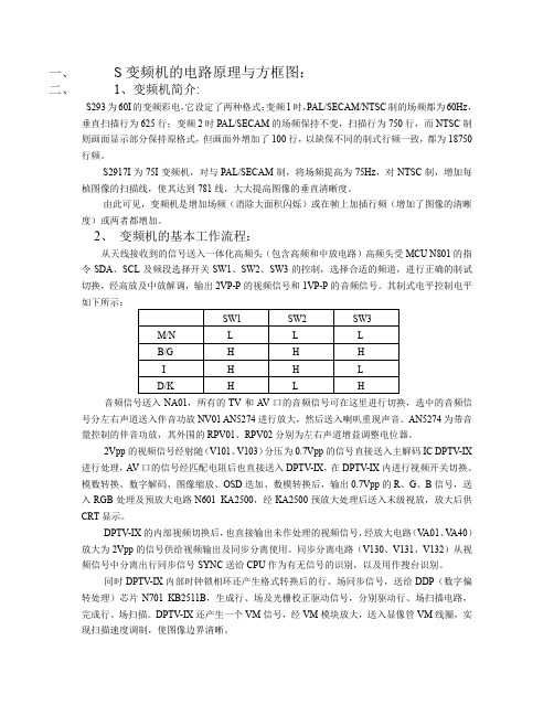
MT5325HDMI1YPbPr#0I2SPWM AR/L0PWM AR/L1MT5325BGAHeadPhoneTuner MPX/IF+/-ADC_IN R/L x 7MT5325 BGALM4558VGAVideo SystemSOY0,CVBS2PY0P,VDAC_OUT1COM0,ADIN0PB0P PR0PAudio SystemAV#1CVBS0PLM4558AUDIO OUTUSB#1USB#2HSYNC VSYNC RP,GP,BPVGACOM SOG VGASDA VGASCLRX_0RX_0B RX_1RX_1B RX_2RX_2B RX_C RX_CBUSB_DP0USB_DM0USB_DP1USB_DM1GPIO_7GPIO_8OPCTRL0OPCTRL1OPCTRL2OPCTRL3MUTE_CTL ADIN0ADIN1ADIN2ADIN3ADIN4ADIN5USB_PWR_EN1OPWM0OPWM1OPWM2USB_PWR_EN0Light-Sensor USB_OC_COMFunction define POWER_LED Key PAD 15325 GPIO Definition PIN NAME NET NAME GPIO_0GPIO_1GPIO_2GPIO_3GPIO_4GPIO_5GPIO_6strap[1]strap[0]GPIO_16GPIO_17SYS_EEPROM_WPBL_ON/OFF HPDET#GPIO_9GPIO_10GPIO_11GPIO_12GPIO_13GPIO_14GPIO_15GPIO_18PHY_DE GPIO_20GPIO_21GPIO_19GPIO_22GPIO_23LVDS_PWR_ENOPCTRL4OPCTRL5OPCTRL6BL_DIMMINGMT5325BGAMini_LVDS Mini_LVDSLVDS1LVDS2Display SystemASPDIFstrap[2]SPEAKERTAS57071、索引ISE NS ETR AI NI NG3、调试接口、与主芯片MT5325接口、FLASH、EEPROM、复位及供电部分电路4、主芯片MT5325网络接口、遥控控制、按键及以太网物理层接口部分电路5、高频电子调谐器、33V升压电路及外围匹配网络部分电路I SG6、YPbPr/AV端子输入、与主芯片MT5325接口及外围匹配网络部分电路7、VGA端子输入及外围匹配网络部分电路8、音频前置放大、耳机功放、光纤输出、与主芯片MT5325接口、耳机输出及外围匹配网络部分电路VPA 9、伴音功放、开/关机静音、重低音功放及外围匹配网络部分电路I10、HDMI输入、切换及外围匹配网络部分电路I11、DDR3存储器、与主芯片MT5325接口及外围匹配网络部分电路(1)12、DDR3存储器、与主芯片MT5325接口及外围匹配网络部分电路(2)I13、LVDS接口、与主芯片MT5325接口及外围匹配网络部分电路14、USB输入接口、与主芯片MT5325接口及外围匹配网络部分电路。
常用电动车充电器根据电路结构可大致分为两种。
第一种是以uc3842驱动场效应管的单管开关电源,配合LM358双运放来实现三阶段充电方式。
其电原理图和元件参数见图表1)欧阳光明(2021.03.07)图表 1 220v交流电经T0双向滤波抑制干扰,D1整流为脉动直流,再经C11滤波形成稳定的300V左右的直流电。
U1 为TL3842脉宽调制集成电路。
其5脚为电源负极,7脚为电源正极,6脚为脉冲输出直接驱动场效应管Q1(K1358) 3脚为最大电流限制,调整R25(2.5欧姆)的阻值可以调整充电器的最大电流。
2脚为电压反馈,可以调节充电器的输出电压。
4脚外接振荡电阻R1,和振荡电容C1。
T1为高频脉冲变压器,其作用有三个。
第一是把高压脉冲将压为低压脉冲。
第二是起到隔离高压的作用,以防触电。
第三是为uc3842提供工作电源。
D4为高频整流管(16A60V)C10为低压滤波电容,D5为12V稳压二极管,U3(TL431)为精密基准电压源,配合U2(光耦合器4N35) 起到自动调节充电器电压的作用。
调整w2(微调电阻)可以细调充电器的电压。
D10是电源指示灯。
D6为充电指示灯。
R27是电流取样电阻(0.1欧姆,5w)改变W1的阻值可以调整充电器转浮充的拐点电流(200-300 mA)。
通电开始时,C11上有300v左右电压。
此电压一路经T1加载到Q1。
第二路经R5,C8,C3, 达到U1的第7脚。
强迫U1启动。
U1的6脚输出方波脉冲,Q1工作,电流经R25到地。
同时T1副线圈产生感应电压,经D3,R12给U1提供可靠电源。
T1输出线圈的电压经D4,C10整流滤波得到稳定的电压。
此电压一路经D7(D7起到防止电池的电流倒灌给充电器的作用)给电池充电。
第二路经R14,D5,C9, 为LM358(双运算放大器,1脚为电源地,8脚为电源正)及其外围电路提供12V工作电源。
D9为LM358提供基准电压,经R26,R4分压达到LM358的第二脚和第5脚。