MAX1978中文数据手册
- 格式:docx
- 大小:358.63 KB
- 文档页数:17
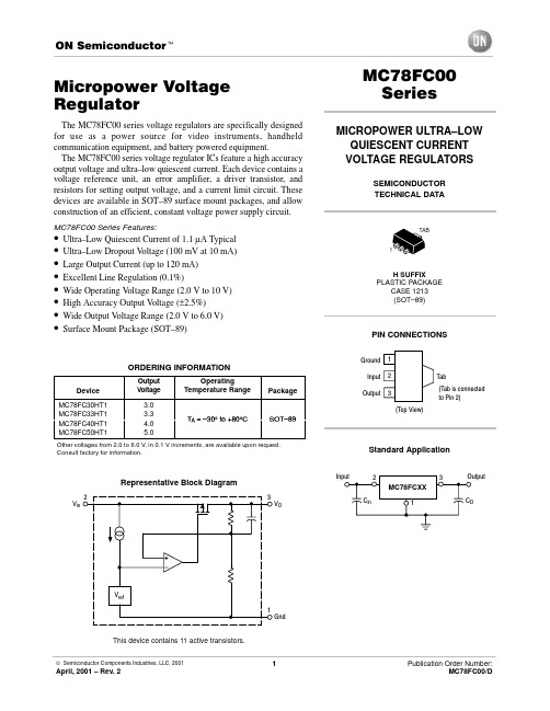
Micropower Voltage RegulatorThe MC78FC00 series voltage regulators are specifically designed for use as a power source for video instruments, handheld communication equipment, and battery powered equipment.The MC78FC00 series voltage regulator ICs feature a high accuracy output voltage and ultra–low quiescent current. Each device contains a voltage reference unit, an error amplifier, a driver transistor, and resistors for setting output voltage, and a current limit circuit. These devices are available in SOT–89 surface mount packages, and allow construction of an efficient, constant voltage power supply circuit.MC78FC00 Series Features:•Ultra–Low Quiescent Current of 1.1 µA Typical •Ultra–Low Dropout V oltage (100 mV at 10 mA)•Large Output Current (up to 120 mA)•Excellent Line Regulation (0.1%)•Wide Operating V oltage Range (2.0 V to 10 V)•High Accuracy Output V oltage (±2.5%)•Wide Output V oltage Range (2.0 V to 6.0 V)•Surface Mount Package (SOT–89)ORDERING INFORMATIONOther voltages from 2.0 to 6.0 V, in 0.1 V increments, are available upon request.Consult factory for information.Representative Block DiagramThis device contains 11 active transistors.V inGndV OMAXIMUM RATINGS (T C = 25°C, unless otherwise noted.)Rating Symbol Value Unit Input Voltage V CC10Vdc Power Dissipation and Thermal CharacteristicsMaximum Power DissipationCase 1213 (SOT–89) H Suffix P D300mW Thermal Resistance, Junction–to–Ambient RθJA333°C/W Operating Junction Temperature T J125°C Operating Ambient Temperature T A–30 to +80°C Storage Temperature Range T stg–40 to +125°C NOTE:ESD data available upon request.ELECTRICAL CHARACTERISTICS(V in = V O+ 1.0 V, I O= 10 mA, T J = 25°C [Note 1], unless otherwise noted.)Characteristic Symbol Min Typ Max Unit Output Voltage V O V 30HT1 Suffix (V in= 5.0 V) 2.925 3.0 3.07533HT1 Suffix (V in = 6.0 V) 3.218 3.3 3.38240HT1 Suffix (V in = 7.0 V) 3.900 4.0 4.10050HT1 Suffix (V in= 8.0 V) 4.875 5.0 5.125Line Regulation Reg line–0.1–mV V in= [V O + 1.0] V to 10 V, I O = 10 mALoad Regulation Reg load–4080mV V in= [V O + 1.0], I O = 1.0 to 10 mAOutput Current I O mA 30HT1 Suffix (V in= 5.0 V)5080–33HT1 Suffix (V in = 6.0 V)65100–40HT1 Suffix (V in = 7.0 V)65100–50HT1 Suffix (V in= 8.0 V)80120–Dropout Voltage V in – V O–0.50.7VI O = 40 mAQuiescent Current I CCµA 30HT1 Suffix (V in= 5.0 V)– 1.1 3.333HT1 Suffix (V in = 5.0 V)– 1.1 3.340HT1 Suffix (V in = 6.0 V)– 1.2 3.650HT1 Suffix (V in= 7.0 V)– 1.3 3.9Output Voltage Temperature Coefficient T C–±100–ppm/°C NOTE: 1.Low duty pulse techniques are used during test to maintain junction temperature as close to ambient as possible.DEFINITIONSDropout Voltage – The input/output voltage differential at which the regulator output no longer maintains regulation against further reductions in input voltage. Measured when the output drops 100 mV below its nominal value (which is measured at 1.0 V differential), dropout voltage is affected by junction temperature, load current and minimum input supply requirements.Line Regulation – The change in output voltage for a change in input voltage. The measurement is made under conditions of low dissipation or by using pulse techniques such that average chip temperature is not significantly affected.Load Regulation – The change in output voltage for a change in load current at constant chip temperature. Maximum Power Dissipation – The maximum total device dissipation for which the regulator will operate within specifications.Quiescent Bias Current – Current which is used to operate the regulator chip and is not delivered to the load.I O , OUTPUT CURRENT (mA)V reg , SET OUTPUT VOLTAGE (V)I T A , AMBIENT TEMPERATURE (°C)V O , O U T P U T V O L T A G E (V )Figure 1. Output Voltage versus Output Current I O , OUTPUT CURRENT (mA)Figure 2. Dropout versus Set Output VoltageFigure 3. Quiescent Current versus Temperature Figure 4. Dropout Voltage versus Output CurrentC C , Q U I E S C E N T C U R R E N T (m A )I N P U T V O L T A G E /O U T P U T V O L T A G E (V )t, TIME (ms)Figure 5. Line Transient ResponseAPPLICATIONS INFORMATION IntroductionThe MC78FC00 micropower voltage regulators arespecifically designed with internal current limiting and lowquiescent current making them ideal for battery poweredapplications. An input bypass capacitor is recommended ifthe regulator is located an appreciable distance (≥ 4 inches)from the input voltage source. These regulators require0.1 µF capacitance between the output terminal and groundfor stability. Most types of aluminum, tantalum or multilayerceramic will perform adequately. Solid tantalums or otherappropriate capacitors are recommended for operation below 25°C. The bypass capacitors should be mounted with the shortest possible leads or track lengths directly across the regulator input and output terminals.With economical electrolytic capacitors, cold temperature operation can pose a serious stability problem. As the electrolyte freezes, around –30°C, the capacitance will decrease and the equivalent series resistance (ESR) will increase drastically, causing the circuit to oscillate. Quality electrolytic capacitors with extended temperature ranges of –40° to +85°C are readily available. Solid tantalum capacitors may be the better choice if small size is a requirement. However, a maximum ESR limit of 3.0 Ω must be observed over temperature to maintain stability. Figure 6 is a typical circuit application. Figure 7 is a current boost circuit which can deliver more than 600 mA. The circuit has no current limiting and the external transistor must be rated for the expected power dissipation.Figure 6. Typical ApplicationV OGnd VFigure 7. Current Boost CircuitO V inPACKAGE DIMENSIONSH SUFFIXPLASTIC PACKAGECASE 1213–01(SOT–89)ISSUE OON Semiconductor and are trademarks of Semiconductor Components Industries, LLC (SCILLC). SCILLC reserves the right to make changes without further notice to any products herein. SCILLC makes no warranty, representation or guarantee regarding the suitability of its products for any particular purpose, nor does SCILLC assume any liability arising out of the application or use of any product or circuit, and specifically disclaims any and all liability, including without limitation special, consequential or incidental damages. “Typical” parameters which may be provided in SCILLC data sheets and/or specifications can and do vary in different applications and actual performance may vary over time. All operating parameters, including “Typicals” must be validated for each customer application by customer’s technical experts. SCILLC does not convey any license under its patent rights nor the rights of others.SCILLC products are not designed, intended, or authorized for use as components in systems intended for surgical implant into the body, or other applications intended to support or sustain life, or for any other application in which the failure of the SCILLC product could create a situation where personal injury or death may occur. Should Buyer purchase or use SCILLC products for any such unintended or unauthorized application, Buyer shall indemnify and hold SCILLC and its officers, employees, subsidiaries, affiliates, and distributors harmless against all claims, costs, damages, and expenses, and reasonable attorney fees arising out of, directly or indirectly, any claim of personal injury or death associated with such unintended or unauthorized use, even if such claim alleges that SCILLC was negligent regarding the design or manufacture of the part. SCILLC is an Equal Opportunity/Affirmative Action Employer. PUBLICATION ORDERING INFORMATIONCENTRAL/SOUTH AMERICA:Spanish Phone:303–308–7143 (Mon–Fri 8:00am to 5:00pm MST)Email:ONlit–spanish@Toll–Free from Mexico: Dial 01–800–288–2872 for Access –then Dial 866–297–9322ASIA/PACIFIC: LDC for ON Semiconductor – Asia SupportPhone:1–303–675–2121 (Tue–Fri 9:00am to 1:00pm, Hong Kong Time)Toll Free from Hong Kong & Singapore:001–800–4422–3781Email: ONlit–asia@JAPAN: ON Semiconductor, Japan Customer Focus Center4–32–1 Nishi–Gotanda, Shinagawa–ku, Tokyo, Japan 141–0031Phone: 81–3–5740–2700。

基于MAX1978的热电偶传感器冷端恒温控制王建华【摘要】热电偶冷端温度恒定性是影响热电偶测温准确性的重要因素之一,设计了一种基于MAX1978的恒温控制系统.采用TEC开关模式,通过PID补偿网络实现TEC控制.【期刊名称】《机械管理开发》【年(卷),期】2012(000)005【总页数】2页(P133,135)【关键词】热电偶;冷端温度;MAX1978【作者】王建华【作者单位】太原理工大学计算机科学与技术学院,山西太原030024【正文语种】中文【中图分类】TH8110 引言热电偶传感器的冷端(参考端)的温度恒定直接影响热电偶的测量精度。
使用半导体致冷器ETC实现热电偶传感器的冷端温度恒定控制,控制精度高,且不受气压等环境因素影响,方便应用于工业现场环境。
1 热电偶测温原理两种不同材料的导体(或半导体)组成一个闭合回路,当两接点温度T和T 0不同时,则在该回路中就会产生电动势,这种现象称为热电效应,该电动势称为热电势。
这两种不同材料的导体或半导体的组合称为热电偶,导体A、B称为热电极。
两个接点,一个称热端,又称测量端或工作端,测温时将它置于被测介质中;另一个称冷端[1],又称参考端或自由端。
热电偶回路中产生的总热电势为:e AB(T,T 0)=e AB(T)+e B(T,T 0)-e AB(T 0)-e A(T,T 0)式中:e AB(T)和e AB(T 0)是接触电势;e A(T,T 0)和e B(T,T 0)是温差电势。
在总热电势中,温差电势比接触电势小很多,可忽略不计,则热电偶的热电势可表示为:e AB(T,T 0)=e AB(T)-e AB(T 0)当参考端温度T 0恒定时,e AB(T 0)=c为常数,则总的热电动势就只与温度T成单值函数关系,即e AB(T,T 0)=e AB(T)-c=f(T)这个关系通常用分度表的形式,由热电偶厂家提供,因此,只要测出e AB(T,T 0)的大小,就能得到被测温度T,此即热电偶测温原理。

如何控制和补偿半导体制冷器摘要在很多需要精密温度控制的设备中经常可以看到半导体制冷器;对温度及其敏感的组件往往与TEC和温度监视器集成到一个单一热工程模块;半导体制冷器也可以通过翻转电流而制热;TEC非常小的体积为精密控制单个组件例如,光纤激光器驱动器,高精度的参考电压或任何温度敏感型设备的温度提供了可能;此应用手册简要讨论TEC设计的起源和历史,然后概述了TEC基本操作;随后又说明了TEC的控制和补偿问题;该文最后详细分析了TEC控制的优化以及优化方程;关键字:PID、DWDM、SFF、SFP、光纤、激光模块、热电冷却器,热电偶、TEC,温度控制,热循环热敏电阻简介1821年托马斯· 塞贝克发现,两个不同的材料的导体连在一起,并且两个材料各自的温度不同的时候,这个环路内就会有电流流过;十二年后,皮尔贴发现了与这一现象相反的效果:通过削减环路中的一个导体,使外部电流流经环路,然后就可以发现两个连接点之间有温度差出现,这一现象后来被称作皮尔贴效应;由于那时的材料所限,皮尔贴效应中材料之间的温度差有大部分都是大电流流过材料所产生的电阻热;随着近来材料学的不断进步,这些连接点制热或制冷的效应越加变得实用化,它可以作为热电泵,使用起来和基于氟碳蒸气压缩的制冷方式并没有太大的差别;虽然TEC仍然不如氟碳蒸发循环设备更加实用,但是它没有移动部件和工作流体,这就为制冷设备小型化提供了可能;基本工作原理由于皮尔贴效应可以通过电流线性控制,半导体制冷器TEC已经在涉及精密温度控制的设备中得到了大量的应用;温度敏感型器件、TEC、温度传感器被集成到一个单一的模块中; TEC控制需要一个电平可以翻转的电源以提供正电压和负电压;要想在单电源设备中做到这一点,那么完全可以使用H桥电路;线性稳压电源总会有纹波,同时它的效率非常低,需要大体积的元件并且还要做好热隔离防止调整管发出的热量加载到制冷器上;但是两个有着互补驱动的同步降压电路能够从单电源获得双电源,同时使单一正电源供电有更高的效率;强外加的脉冲宽度调制PWM控制两个输出电压,使流经TEC的电流改变大小和方向;通过电流的不断改变,小体积的TEC可以高精度控制各种分立器件的温度,如光纤激光驱动器,精密电压基准,或任何其它的温度敏感型器件;也可以通过翻转流经TEC的电流使它制热;TEC功率控制MAX1968和MAX1978是一种用来驱动基于皮尔贴效应的半导体制冷器的高集成度H桥PWM开关式驱动芯片;MAX1968是一个符合成本效益的解决方案,因为它集成了4个电源开关控制和PWM控制,它采用28引脚耐热增强型TSSOP-EP封装;MAX1978而是48引脚TQFN-EP 封装,它包括MAX1968所有的电路,以及建立热反馈回路的放大器; MAX8520和MAX8521分别采用采用20引脚TQFN封装MAX8520和36焊球WLP封装MAX8521,提供了最小的PCB封装解决方案;MAX1978裸露的散热片使其包装可耗散热量高达,并且内部集成有电压转换模块,可以从单一5V电源的到双极±3V,驱动电流3A的电压;开关频率可以在500kHz或1MHz切换;独立的正和负输出电流阈值和电压阈值控制电路已经在芯片上集成,并且可以通过外部电阻器对其进行设定;模拟控制信号精确地设置流经TEC电流的大小而不关注TEC两端的电压;高度集成的MAX1978提供了成本合理,体积合适的驱动控制TEC的解决方案,并且这一方案的控制闭环只需要一些无源外部元件;使用控制闭环来调节TEC温度为了达到精密控制温度的目的,需要TEC模块内或附近的温度监视器发送温度信息与基准相比较,产生一个误差信号;该误差信号被放大,并发送到TEC; TEC然后制热或制冷以改变器件温度,本地监控温度随之改变从而完成循环;如同任何控制回路,稳态精度与DC环路增益密切相关;由于大量杂散热量的原因,环路对TEC 温度变化的反应时间可能要有几十秒之多;因此,TEC和监控回路需要一个补偿电路以避免振荡和过冲;又因为最终积分器需要大的时间常数,很难找到大容量的电容器同时具有足够的低泄漏,以实现高的直流增益;因此,要实现稳定,最小尺寸的积分电容必须认真选择;要想对热闭环进行补偿,就必须理解的TEC模块的热响应;可以通过使用MAX1968或MAX1978作为一个驱动器测量的TEC模块的低频响应、在该模块的内部的热敏电阻,或者亚赫兹像能力和网络分析仪如同安捷伦HP3562A动态信号分析仪;大多数激光二极管TEC模块的性能大都接近双极型系统two-pole的行为的系统;第一极在20mHz,第二极在1Hz;如果没有网络分析仪,那么测量直流增益时可认为TEC的响应极点为20mHz和1Hz;虽然这个模型是很粗糙的,但是它可以帮助我们了解在完善闭环时的极限;由于模块有一个缓慢的20mHz的极,频率上升到1Hz后大约有90度的相移;由此可以看出,第二个极有一个潜在的振荡条件;在制冷模式下的TEC的响应如图1中的实线图形所示;由于TEC在同等电流注入下,制热能力是制冷能力的四倍,制冷制热频率响应相差大概有6dB;该模块的其他因素,如散热,环境温度,和内部产生的热量,也可能改变响应曲线;从不同的模块制造商也会有不同的反应;如果一个TEC模块没有内部的热敏电阻,所用的TEC 和热敏电阻的频率响应要单独测定;图1 TEC频率响应补偿回路比例积分微分PID控制器,如图2所示,是一个很好补偿方法;在这里可以对电路进行调整优化TEC响应;为了达到高的直流增益,积分器是必要的;在图2中的积分器是由C2构成的,并且积分器添加了响应曲线的第三极,R3使得电路更加使得稳定;R3插入一个零到之前的积分单位增益交叉;理想情况下,这应该发生在第一极点20mHz;并且可以推高到70mHz而没有任何稳定性问题;虽然这个过程中创建了一个从20mHz到70mHz的二阶响应,但是相位从未达到振荡条件180度;如图1中的红色虚线所示;图2 PID控制器的电路;图2中由C1,R1和R2形成的差分网络,又增加了零点来抹去第二1Hz的极点;这个零点提供了额外的相位裕度,使闭环在在更高的频率处截止;如图1中所示的蓝色虚线;虽然具有高环路带宽的快速响应是不需要的,高DC增益和小电容却是必不可少的;该补偿器使用C3使增益衰减到30Hz,从而减少噪声注入闭环;在TEC的应用中,这允许闭环在2Hz交叉,并为闭环在很宽的范围内提供良好的相位裕度; 图三所示TEC热闭环中为2Hz的交叉补偿的例子;尽量选择高阻值的R3以使积分电容C2尽可能小;然而这种方法也有弊端,它会使得PID的增益变小;因为我们必须在70mHz插入一个零点,我们使用关系:FZ1 = 1 /2π×C2×R3图3 热闭环原理简图前文已经说过,FZ1 = 70mHZ,如果选择R3 =243kΩ,那么C2 就应为μF;我们选择10μF设计;现在我们选择R1 =10kΩ;这使得前端放大器U2有足够的增益以减少反射积分器U1的错误,同时保持合理的电容器的尺寸;现在,我们必须插入一个零点以抹去第二个在1Hz的TEC响应曲线极点;因为我们希望得到良好的相位裕度,零插入所需的交叉频率除以至少5或;这给出了一个在交叉频率的一个更好的相位裕度;然后通过放置由R1创建的、至少5倍于交叉频率,或者10Hz的极点终止该零点;这限制了积分器的的增益;所以,因为:FZ2 = 1 /2π×C1×R2并且FZ2 = 和R2 =510KΩ,我们可以算出C1 =μF;我们选择C1为1μF;为了计算出R1的大小,我们使用关系:F3 = 1 /2π×C1×R1因为F3 =10HZ,C1 =1μF,这样我们可以知道R1 =Ω;使用10kΩ就可以提供更好的相位裕度;然后,我们必须设置衰减频率在30Hz;因为R3 =243kΩ,FC = 30Hz,并且:FC= 1 /2π×C3×R3我们知道C3 =μF;现在,TEC的响应已被优化,然后系统的增益必须进行调整,应在2Hz交叉,从图1中我们可以看到,在2Hz的未补偿产地函数中图中实线1具有-30dB的增益;如果我们希望有一个2Hz的单位增益交叉,我们必须在2Hz处提供+30 dB的增益;由于U1及其组成部分在2Hz有增益,我们必须在所需的系统增益总额中减去此增益从而找到前端增益;U1的增益由R3和C1决定;在2Hz处,R1、R2、C2和C3完全可以忽略;C1在2Hz阻抗可以由下式获得,即:XC =-j /2π×FC×C1因为C1 = 1μF,FC = 2Hz,那么:XC = ΩU1的幅度增益G为:G = | R3 / XC |由于R3 =243kΩ,XC =Ω,G = 或分贝;要想对此增益进行全面的分析,就不应忽视R1、R2、C2和C3,此时G = 或分贝,从而验证了我们的假设;现在,我们必须在前端再提供分贝的增益以完成2Hz处的增益交叉;前端增益部分有两个功能:它减少积分器U1产生的误差,和采集从热敏电阻传来的温度信息; 由R4、R5和U2图3所设定的直流增益需要足够高以防止该误差信号被PID补偿电路消除;由于R4 =10kΩ,R5 =100kΩ,那么前端增益是11或分贝,足以压倒分贝的PID补偿部分;从热敏电阻传来的温度读数以误差信号的形式被传递给PID控制部分;该误差信号表示的是实际温度和所需温度设定值之间的差异;U2输出的误差信号可以按照下式计算:这里的是通过10kΩ的电阻器连接到热敏电阻的参考值,RT是电阻热敏电阻,VSET是电压设定点;调节TEC温度的热闭环整个环路以及补偿值的例子如图3所示;通过了解在一个给定的温度下RT阻值的大小,可根据需要选择设定VSET的值,然后自动调节温度;此处使用一个跳线可选式数字-模拟转换器DAC或电位器来控制VSET;通过发送误差信号到PID调节补偿部分,然后它控制输入到到TEC驱动器的模拟信号,直到温度误差信号接近0,由此,器件的温度得以调节;由于PID补偿部分有着良好的相位裕度,该电路足以应对TEC增益在加热或冷却模式的变化;组件的选择该电路的组件选择将取决于所需的应用程序的具体要求;MAX1978提供有这种设计拓扑结构所需要的片上放大器;如果使用MAX1968,MAX8520,或MAX8521的话,那么就需要使用一个具有低失调电压漂移的运算放大器,例如MAX4477ASA就是一个不错的选择;由于上面的热敏电阻的信号电平比较低,电路中热敏电阻的信号应该使用屏蔽线; U1应该选用超低漏电电流的型号,以避免高电路阻抗所产生的直流漂移; MAX4475ASA运算放大器的漏电电流仅仅只有150pA最大值,所以它确实是一个不错的选择; U1周围的元件,特别是C2和C3,应选择具有最高的漏电阻的型号,C2需要尽可能最低的热漂移;聚苯乙烯薄膜电容器是最好的选择,但他们是非常庞大和昂贵;陶瓷电容器一个不错的选择,但较大的值可能会泄漏到足以引起增益误差;不要使用电解电容或钽电容器;U1反向端引脚的周围和下面应放置一个带有PC板的保护环,并且它的组件应该被连接到U1的同相端;保护环拦截任何可能引起求和误差的杂散电流;助焊剂,湿气,和玻璃纤维印刷电路板可以引起漏电流的问题,而保护环可以改善这些影响;保形涂层板及其组件可以帮助防止污染物干扰电路的性能;TEC控制回路的测试控制回路可以通过单位阶跃函数来测试;一个简单的温度设定点的变化应使热敏电阻有所反应,并使得新的温度设定点与之前相比有着非常小的过冲;如果阶跃响应观察到振铃现象,表示在交叉频率相位裕度比较差;通过记录振铃频率和振铃次数,可对直流增益交叉频率或者补偿电路进行调整,直至得到得到一个令人满意的结果;通过使用这种方法与一些TEC行为的观察,一个TEC的闭环可以在未经补偿网络分析仪测试的情况下得到补偿;即使有了网络分析仪的帮助,该系统应该在制冷和制热两种模式下利用阶跃响应的方法进行测试;在制冷模式下加热,在加热模式下的制冷是系统环境最为恶劣的情况; 闭环中的直流误差可以通过输入电阻为1G Ω的一个6位数计进行测量,例如可以利用Agilent 34401A来测定设定值和热敏电阻输出值之间的差异图3;这个差异应该在100μV范围内;噪声可以在相同的点利用差分放大器来测量,如泰克ADA400A; 在100Hz的带宽下,误差值应该在20μ以内;VP-P结论精密热控制将会继续使用半导体制冷器作为一种解决方案;可以预见TEC的性能将继续提高,使它在范围逐渐增广的温控领域成为一种们更具吸引力的解决方案;TEC甚至可能取代蒸汽循环制冷装置用来加热和冷却室内环境;TEC驱动器和热控制回路才刚刚开始开始实际应用;注:安捷伦是安捷伦科技公司的注册商标和注册服务标志Tektronix是泰克公司的注册商标和注册服务商标。

简单的限流开关模式Li +电池充电控制器--------------------------------------------------------------------------概述低成本的MAX1873R/S/T提供所有功能需要对高达4A或以上的2 - ,3 - 或4 - 系列的锂离子电池进行简单而有效的充电。
它提供调节充电电流和电压,少于±0.75%时,总电压在电池端出现错误。
在降压的DC - DC配置下,外部P沟道MOSFET有效地为电池充电,这是低成本的设计。
MAX1873R/S/T使用两个控制回路调节电池电压和充电电流,一起工作的两个控制回路在电压和电流调节之间顺利转换。
一个额外的控制回路限制电流来自输入端,可以使AC适配器尺寸和成本最小化。
模拟电压还提供其输出正比于充电电流,以便ADC或微控制器可以监控充电电流。
在多化学充电器设计时,MAX1873也可能被用来作一个有效的有限电流源对镍镉或镍氢电池充电。
MAX1873R/S/T采用节省空间的16引脚QSOP封装是可用的。
使用评估板(MAX1873EVKIT),可以帮助减少设计时间。
--------------------------------------------------------------------------应用笔记本电脑便携式网络片2 - ,3 - ,或4节锂离子电池充电器6 - ,9 – 10节镍电池充电器手持式仪表便携式桌面助理(PDA)台式插座充电器引脚配置在数据资料的最后。
--------------------------------------------------------------------------特征•低成本和简单电路•可对2 - ,3 - ,或4节串联锂离子电池充电•AC适配器输入电流限制回路•还可对以镍为主的电池充电•模拟输出监视充电电流•± 0.75%的电池调节电压•5μA关断电池电流•输入电压高达28V•200mV的压差电压/100%占空比•可调充电电流•为300kHz的PWM振荡器降低了噪音•采用节省空间的16引脚QSOP•采用MAX1873评估板以加快设计----------------------------------------------------------------------订购信息部分温度 .范围 PIN的封装MAX1873REEE -40 °C至85 °C 16 QSOPMAX1873SEEE-40 °C至85 °C16 QSOPMAX1873TEEE-40 °C至85 °C16 QSOP------------------------------------------------------------------典型工作电路极限值CSSP,CSSN,DCIN接GND ·······················- 0.3V至30V VL,ICHG / EN接GND ························- 0.3V至6V VH,EXT接DCIN ····························- 6V至0.3V VH,EXT接GND ·······················( V DCIN 0.3V) - 0.3V EXT接VH ······························6V至- 0.3V DCIN接VL······························30V至- 0.3V VADJ,REF,CCI,CCV,CCS, IOUT接GND··············- 0.3V至(VL 0.3V)BATT,CSB接GND···························- 0.3V至20V CSSP接CSSN·····························- 0.3V至0.6V CSB接BATT·····························- 0.3V至0.6V VL源电流··································+50mA VH反向电流································+40mA 连续功耗(TA=70℃)16引脚QSOP封装(在70° C以上,功率衰减8.3mW/° C···········+667mW 工作温度范围MAX1873_EEE·····················-40°C至+85°C 结点温度································+150 °C 存储温度范围··························-65°C至+150°C 引线温度(焊接,10S)···························300°C 超出“绝对最大额定值”中所列的压力可能会造成设备的永久性损坏。

高精度半导体激光器驱动电源及温控电路设计罗亮;胡佳成;王婵媛;刘泽国【摘要】In order to solve the problem that the output power and wavelength of semiconductor laser light source was easily influenced by drive current and working temperature in Brillouin optical fiber sensing system, high-precision constant current drive and temperature control circuit were designed.Deep negative feedback integrated circuit was used to control the laser drive current precisely.Integrated temperature control chip MAX1978 was adopted to control the working current of semiconductor coolers and achieve the accurate controlment of laser working temperature.The results show that the design achieves the adjustment of drive current from 0mA~100mA.The maximum relative error of current control is 0.06%, current stability is 0.02% and the maximum error of temperature control is 0.03℃.Under the condition of temperature control, the stability of optical power is 0.5%, and the largest drift is0.005dBm.The design can achieve the effective control of current and temperature and ensure the stability of output light.%为了解决布里渊光纤传感系统中半导体激光器光源输出功率和波长易受驱动电流和温度影响的问题,设计了一种高精度恒流驱动和温控电路.该电路利用深度负反馈积分电路对激光器驱动电流进行精密的恒流控制,同时采用集成温度控制芯片MAX1978控制半导体制冷片的工作电流,实现对激光器工作温度的精确控制.结果表明,本设计实现了驱动电流0mA~100mA可调,电流控制最大相对误差为0.06%,电流稳定度为0.02%,温度控制最大误差为0.03℃,在温控的条件下,光功率稳定性达到0.5%,最大漂移量为0.005dBm.该设计实现了对电流和温度的有效控制,保证了输出光的稳定性.【期刊名称】《激光技术》【年(卷),期】2017(041)002【总页数】5页(P200-204)【关键词】激光技术;半导体激光器;恒流驱动;温控电路;布里渊传感【作者】罗亮;胡佳成;王婵媛;刘泽国【作者单位】中国计量大学计量测试工程学院,杭州 310018;中国计量大学计量测试工程学院,杭州 310018;中国计量大学计量测试工程学院,杭州 310018;中国计量大学计量测试工程学院,杭州 310018【正文语种】中文【中图分类】TN86;TP273布里渊分布式光纤传感因能同时远距离传感温度和应变,被广泛应用在天然气和石油管道、远距离电力传输线路检测、矿井安全和边境安全监控等领域[1-3],具有广阔的发展空间。


MAX15301是一个全功能,高效,数字化的点负载(POL)操纵器与先进的电源治理和遥测功能与PID 为基础的数字电源稳压器,MAX15301采纳Maxim拥有专利的Intune的™自动补偿,状态空间操纵算法。
Intune 的操纵律是有效的小信号和大信号响应,占占空比饱和度的阻碍。
这排除需要用户以确信和设置的阈值从线性转换到非线性模式。
这些能力在快速环路的瞬态响应,并减少输出电容器的数量相较,竞争的模拟和数字操纵器。
MAX15301包括多种功能,以优化效率。
内部开关BabyBuck的稳压器可产生栅极驱动器和内部偏置电源,低功耗的操纵器。
一种先进的,高效率的MOSFET的栅极驱动器,具有自适应非重叠按时,而持续调整的高侧和低侧的按时和驱动电压的全范围内的电压,电流和温度,以尽可能减少开关损耗。
MAX15301设计最终客户的设计环境的初衷。
上的PMBus™兼容的串行总线接口进行通信的监控器监控和故障治理。
全套的电源治理功能,无需复杂和昂贵的测序和监控IC。
大体的DC-DC转换操作,可设置通过引脚搭接,并非需要用户配置固件。
这使得电源子系统的快速进展前完成板级系统的工程。
Maxim提供支持的硬件和软件配置MAX15301 ,MAX15301可在32引线,5mm×5mm TQFN封装,工作在-40°C至+85°C的温度范围内。
特点:的自动补偿功能能够确保稳固,同时优化瞬态性能2.在快速瞬态响应减少输出电容的非线性补偿结果3.差分远端电压传感许诺±1%V OUT精度在整个温度范围内(-40°C至+85°C)接口用于配置,操纵和监测5.支持电压定位6.提高效率(自适应非重叠时序驱动器)至14V的宽输入电压范围8.高效片上BabyBuck稳压器的自偏置9.输出电压范围从到10.进入预偏置输出启动11.可配置的软启动和软停止时刻12.固定工作频率同步(300kHz至1MHz)13.灵活的排序和故障治理14.引脚手动跳线配置(输出电压,从机地址,开关频率,电流限制)15.能够快速原型图表典型工作电路引脚名字功能1SYNC外部开关频率同步输入端。

78M6613 Evaluation BoardUser ManualDecember 2011Rev. 2UM_6613_04578M6613 Evaluation Board User Manual UM_6613_045 © Maxim Integrated The Maxim logo and Maxim Integrated are trademarks of Maxim Integrated Products, Inc.UM_6613_045 78M6613 Evaluation Board User ManualRev. 2 3Table of Contents1Introduction ................................................................................................................................... 5 1.1 Package Contents ................................................................................................................ 5 1.2 System Requirements ........................................................................................................... 5 1.3 Safety and ESD Notes .......................................................................................................... 6 1.4 Firmware Demo Code Introduction ........................................................................................ 6 1.5 Testing the 78M6613 Evaluation Board Prior to Shipping ...................................................... 6 2 Installation . (7)2.1 USB Driver Installation .......................................................................................................... 7 2.2 Confirm COM Port Mapping .................................................................................................. 8 2.3 Basic Connection Setup ........................................................................................................ 9 2.4 Verify Serial Connection to the PC ...................................................................................... 11 2.5 In-Circuit Emulator (ICE) Adaptor ........................................................................................ 13 3 Schematics, Bill of Materials and PCB Layouts . (14)3.1 78M6613 Evaluation Board Schematics .............................................................................. 14 3.2 78M6613 Evaluation Board Bill of Materials ........................................................................ 16 3.3 78M6613 Evaluation Board PCB Layouts ............................................................................ 18 4 Ordering Information ................................................................................................................... 19 5 Contact Information ..................................................................................................................... 19 Revision History . (20)78M6613 Evaluation Board User Manual UM_6613_0454 Rev. 2FiguresFigure 1: 78M6613 Evaluation Board Connections ................................................................................... 9 Figure 2: 78M6613 Evaluation Board Application Diagram ..................................................................... 10 Figure 3: ICE Adaptor ............................................................................................................................ 13 Figure 4: Attaching the ICE Adaptor ....................................................................................................... 13 Figure 5: 78M6613 Evaluation Board Electrical Schematic (1 of 2) ......................................................... 14 Figure 6: 78M6613 Evaluation Board Electrical Schematic (2 of 2) ......................................................... 15 Figure 7: 78M6613 Evaluation Board PCB Top View ............................................................................. 18 Figure 8: 78M6613 Evaluation Board PCB Bottom View (18)TableTable 1: COM Port Setup Parameters .................................................................................................... 11 Table 2: 78M6613 Evaluation Board Bill of Materials (16)UM_6613_045 78M6613 Evaluation Board User ManualRev. 251 IntroductionThe Teridian™ 78M6613 Evaluation Board is an electrical measurement unit for performing measurements of up to two single-phase AC loads. It incorporates the 78M6613 power- and energy-measurement IC and connects to a PC through a USB cable such as the one provided in the demo kit. The Evaluation Board demonstrates the capability of the 78M6613 energy-meter controller chip for measurement accuracy and overall system use.The board is preprogrammed with Firmware Demo Code (file name6613_OMU_S2+2_URT_V1_1x.hex) in the flash memory of the78M6613 IC that allows evaluation of the IC’s capabilities.The 78M6613 energy-measurement data and status is read back overthe serial UART interface using a text-based command line interface(CLI) command set. Easy manual operation is performed usingHyperTerminal. Refer to the applicable 6613_OMU_S2+2_URT_V1_1xFirmware Description Document for invocation usage of the CLIcommands.1.1 Package ContentsThe 78M6613 Evaluation Board Demo Kit includes:•78M6613 Evaluation Board•USB Cable Assembly USB A-B 28/24 1.8M (Tyco/Amp 1487588-3)•CD with documentation1.2 System RequirementsThe 78M6613 Evaluation Board requires use of a PC with the following features:•PC (1 GHz, 1 GB) with Microsoft Windows XP®, Windows Vista®, or Windows 7 operating systems equipped with USB port•Minimum 1024 x 768 video display resolutionTeridian is a trademark of Maxim Integrated Products, Inc.Windows XP and Windows Vista are registered trademarks of Microsoft Corp.78M6613 Evaluation Board User Manual UM_6613_0456Rev. 21.3 Safety and ESD NotesEXERCISE CAUTION WHEN LIVE AC VOLTAGES ARE PRESENT!Standard ESD precautions must be taken when handling electronic equipment. The 78M6613 contains ESD protected interfaces.Do not connect test equipment, ICE emulators or external development boards directly to the 78M6613 hardware. Damage to the 78M6613 and external equipment will occur due to the 78M6613’s “high side” reference topology. The 78M6613’s V3P3 (i.e., “high side”) is connected directly to Neutral (Earth Ground) creating a ground reference disparity with any properly grounded external equipment.The board components and firmware settings are designed to operate with the following nominal AC electrical ranges:Voltage Current Line Frequency110-240 VAC 10 mA – 20A46-64 Hz1.4 Firmware Demo Code IntroductionThe Firmware Demo Code provides the following features:•Basic energy measurement data such as Watts, Volts, current, VAR, VA, phase angle, power factor, accumulated energy, frequency, date/time, and various alarm statuses.• Control of alarm thresholds, calibration coefficients, temperature compensation, etc.The following setup is used to facilitate performance evaluation between the user at the PC host and the firmware code in the board:•The CLI through HyperTerminal or comparable terminal emulator on a different operating system. For information about the CLI, see the applicable Firmware Description Document.The 78M6613 is shipped with Firmware Demo Code Revision 1.0 or later loaded in the 78M6613 chip and included on the CD. The code revision can be verified by entering the command >i via the command line interface. Firmware for the Demo Unit can be updated using either the Teridian TFP2 or an in-circuit emulator such as the Signum Systems ADM51 ( ).1.5 Testing the 78M6613 Evaluation Board Prior to ShippingBefore every 78M6613 Evaluation Board is shipped, the following procedures have been performed at the factory:• Full Calibration – Precise energy source equipment is used to calibrate the current and voltage. The temperature is also calibrated at the same time.• Accuracy Test – This “bench” level test ensures the energy accuracy is within ±0.5%.UM_6613_045 78M6613 Evaluation Board User ManualRev. 2 72 Installation2.1 USB Driver InstallationThis evaluation kit includes an isolated USB interface for serial communications with a PC. The FTDI USB controller IC FT232R performs the USB functions. The FTDI driver for Windows presents a virtual COM port for enabling serial communications. Control of the 78M6613 Evaluation Board can be managed using a terminal emulation program. The FTDI Windows driver is a certified driver for Windows 2000 and Windows XP.1. Upon attaching the 78M6613 Evaluation Board to the PC, the Found New Hardware Wizardautomatically launches and installs the appropriate driver files. If your PC does not find the FTDI driver files on its local hard disk drive, locate and reference the FTDI USB Driver and Utilities subdirectory on the CD. The FT232R controller is powered from the USB cable and is active even when no AC power is applied to the 78M6613 Evaluation Board.Note: If an older FTDI driver has been previously installed, it is recommended to remove the olderversion before installing this newer FTDI driver. Execute the ftdiClean.exe utility from the FTDI USB Driver and Utilities subdirectory.For FTDI driver support on other operating systems, refer to FTDI’s website at (/FTDrivers.htm).78M6613 Evaluation Board User Manual UM_6613_0458 Rev. 22.2 Confirm COM Port Mapping1. Launch the Control Panel and click on the System icon.2. The System Properties screen appears. Click on the Hardware tab. Click on Device Manager .Under Ports (COM & LPT), look for the USB Serial Port assignment.3. Take note of the COM port assignment for the USB Serial Port.UM_6613_045 78M6613 Evaluation Board User ManualRev. 292.3 Basic Connection SetupFigure 1 shows the basic connections of the 78M6613 Evaluation Board for use with external equipment. The 78M6613 Evaluation Board is powered through the USB cable. This same USB cable provides the communications link between the host PC and the 78M6613 Evaluation Board.The 78M6613 Evaluation Board accepts 120 VAC and 230 VAC (nominal) up to 300 VAC (max).Figure 1: 78M6613 Evaluation Board ConnectionsAttach an AC source to J3 (Neutral) and J6 (Line). Attach the AC load to J4 (Neutral) and J8 (Line). Note: The hardware and embedded firmware are capable of measuring two outlets or AC loads. For more information, contact Maxim application support.78M6613 Evaluation Board User Manual UM_6613_045Figure 2: 78M6613 Evaluation Board Application Diagram10 Rev. 2UM_6613_045 78M6613 Evaluation Board User ManualRev. 2112.4 Verify Serial Connection to the PCAfter connecting the USB cable from the 78M6613 Evaluation Board to the host PC, start the HyperTerminal application (or another suitable communication program) and create a session using the communication parameters shown in Table 1.Table 1: COM Port Setup ParametersSetup Parameter Value Port speed (baud) 38400 Data bits 8 ParityNone Stop bits 1 Flow controlNoneHyperTerminal can be found in Windows by selecting Start →All Programs →Accessories → Communications →HyperTerminal . The connection parameters are configured by selecting File → Properties . The New Connection Properties menu appears.Select the appropriate COM port and click Configure . The COMn Properties menu appears.78M6613 Evaluation Board User Manual UM_6613_04512 Rev. 2Note that port parameters can only be adjusted when the connection is not active. It may be necessary to click the Disconnect Button to disconnect the port.FTDI COM Port Trouble-ShootingCLI measurement can be displayed in two different formats: decimal or hex. Both formats are returned as ASCII character strings. The following figure uses CLI commands to return the same data presented in the Auto-Reporting mode.Refer to the applicable Firmware Description Document for a complete description of available CLI commands and their invocation usage.The 6613_OMU_S2+2_URT_V1_1x.hex is compatible with the 78M6612 OMU GUI. Refer to the OMU1-S-WW Demo Unit User Manual for installation and operation instructions applicable to the OMUGUI.Use “?” for Decimal format Use “$” for Hex formatUM_6613_045 78M6613 Evaluation Board User ManualRev. 2132.5 In-Circuit Emulator (ICE) AdaptorThe 78M6613 firmware (stored in internal flash memory) can be updated to accommodate program enhancements. Use the Signum ADM51 or the Teridian TFP-2 to download new firmware to the 78M6613. The supplied ICE Adaptor is required to interface the flat ribbon cable (provided with the ADM51 or TFP-2) to the 78M6613 Evaluation Board.Figure 3: ICE AdaptorFigure 4 shows how to attach the ICE Adaptor to the 78M6613 Evaluation Board. Please make note of the orientation of the ICE Adaptor as to how it attaches to the 78M6613 Evaluation Board (V3P3 ICE Adaptor pin connects to the +V3P3 Evaluation Board pin).Figure 4: Attaching the ICE AdaptorDisconnect the 78M6613 Evaluation Board from live AC voltages before connecting the ADM51 or TFP-2. An Earth ground disparity and high AC voltages are present on the 78M6613 Evaluation Board when it is connected to the AC outlet. Equipment damage to the 78M6613, ADM51/TFP-2 and attached PC may occur when live AC voltages are present on the 78M6613 Evaluation Board. Refer to the 78M6613 Safety Precautions Applications Note for additional information.It is recommended to always use the supplied flat ribbon cable. Do not use discrete wires in place of the flat ribbon. Poor signal integrity will cause flash memory programming errors. Additional adaptors and flat ribbon cables can be ordered through Maxim.Power to the 78M6613 is provided via the USB cable. Attach the USB cable during programming.UM_6613_045 78M6613 Evaluation Board User ManualRev. 2 194 Ordering InformationPART DESCRIPTION 78M6613-EVM-178M6613 Evaluation Board5 Contact InformationFor more information about Maxim products or to check the availability of the 78M6613, contact technical support at /support .78M6613 Evaluation Board User Manual UM_6613_04520 Rev. 2Revision HistoryREVISION NUMBERREVISION DATE DESCRIPTIONPAGES CHANGED1.0 1/11 Initial release1.1 5/11 Updated photos, schematics, BOM, and PCB layouts for the Rev. 7 board.5, 9, 13-18212/11Replaced corporate logo.Revised operating system requirements. Corrected Flow Control value.1 5 11。

Rev. 5.0Features•Output Current up to 0.5A•Output V oltages of 5, 6, 8, 10, 12, 15, 18, 20, 24V •Thermal Overload Protection •Short Circuit Protection•Output Transistor Safe Operating area (SOA)ProtectionDescriptionThe MC78MXX/LM78MXX series of three-terminal posi-tive regulators are available in the TO-220/D-PAK package with several fixed output voltages making it useful in a wide range of applications.TO-220D-PAK1. Input2. GND3. Output11Internal Block DigramMC78MXX/LM78MXX3-terminal 0.5A positive voltage regulatorMC78MXX/LM78MXXAbsolute Maximum RatingsElectrical Characteristics (MC78M05/LM78M05)(Refer to the test circuits, 0 < T J < +125°C, I O =350mA, V I =10V , unless otherwise specified, C I = 0.33µF, C O =0.1µF)Notes:*Load and line regulation are specified at constant junction temperature. Change in V o due to heating effects must be takeninto account separately. Pulse testing with low duty is used.ParameterSymbol Value Unit Input Voltage (for V O = 5V to 18V)(for V O = 24V)V I V I 3540V V Thermal Resistance Junction-CasesR θJC 5°C/W Thermal Resistance Junction-Air (TO-220 Package)R θJA 65°C/W Operating Temperature Range MC78MXX/LM78MXX T OPR 0~ + 125°C Storage Temperature RangeT STG-65~ + 150°CParameterSymbolConditionsMin.Typ.Max.Unit Output VoltageV OT J =+25°C4.855.2VI O = 5 to 350mA V I = 7 to 20V 4.755 5.25Line Regulation ∆V O I O = 200mA T J =+25°CV I = 7 to 25V --100mV V I = 8 to 25V--50Load Regulation ∆V O I O = 5mA to 0.5A, T J =+25°C --100mV I O = 5mA to 200mA, T J =+25 °C --50Quiescent Current I Q T J =+25°C- 4.06mA Quiescent Current Change∆I Q I O = 5mA to 350mA --0.5mAI O = 200mA V I = 8 to 25V --0.8Output Voltage Drift ∆V/∆T I O = 5mAT J = 0 to +125°C -−0.5-mV/°COutput Noise Voltage V N f = 10Hz to 100KHz -40-µVRipple Rejection RR f = 120Hz, I O = 300mA V I = 8 to 18V62--dB Dropout Voltage V D T J =+25°C, I O = 500mA -2-V Short Circuit Current I SC T J =+25°C, V I = 35V -300-mA Peak CurrentI PKT J =+25°C-700-mAMC78MXX/LM78MXXElectrical Characteristics (MC78M06)(Refer to the test circuits, 0 ≤ T J ≤ +125°C, I O =350mA, V I =11V , unless otherwise specified, C I = 0.33µF, C O =0.1µF)Notes:*Load and line regulation are specified at constant, junction temperature. Change in V o due to heating effects must be takeninto account separately. Pulse testing with low duty is used.ParameterSymbolConditionsMin.Typ.Max.Unit Output VoltageV OTJ=+25°C5.7566.25VI O = 5 to 350mA V I = 8 to 21V 5.76 6.3Line Regulation ∆V O I O = 200mA T J =+25°CV I = 8 to 25V --100mV V I = 9 to 25V--50Load Regulation ∆V O I O = 5mA to 0.5A, T J =+25°C --120mV I O = 5mA to 200mA, T J =+25°C --60Quiescent Current I Q T J =+25°C- 4.06mA Quiescent Current Change∆I Q I O = 5mA to 350mA --0.5mAI O = 200mA V I = 9 to 25V --0.8Output Voltage Drift ∆V/∆T I O = 5mAT J = 0 to +125°C -− 0.5-mV/°COutput Noise Voltage V N f = 10Hz to 100KHz -45-µVRipple Rejection RR f = 120Hz, I O = 300mA V I = 9 to 19V59--dB Dropout Voltage V D T J =+25°C, I O = 500mA -2-V Short Circuit Current I SC T J = +25°C, V I = 35V -300-mA Peak CurrentI PKT J =+25°C-700-mAMC78MXX/LM78MXXElectrical Characteristics (MC78M08)(Refer to the test circuits, 0 ≤ T J ≤ +125°C, I O =350mA, V I =14V , unless otherwise specified, C I =0.33µF, C O =0.1µF)Notes:*Load and line regulation are specified at constant, junction temperature. Change in V o due to heating effects must be takeninto account separately. Pulse testing with low duty is used.ParameterSymbolConditionsMin.Typ.Max.Unit Output VoltageV OT J =+25 °C7.788.3VI O = 5 to 350mA V I = 10.5 to 23V 7.688.4Line Regulation ∆V O I O = 200mA T J =+25°CV I = 10.5 to 25V --100mV V I = 11 to 25V--50Load Regulation ∆V O I O = 5mA to 0.5A, T J =+25°C --160mV I O = 5mA to 200mA, T J =+25°C --80Quiescent Current I Q T J =+25°C- 4.06mA Quiescent Current Change∆I Q I O = 5mA to 350mA --0.5mAI O = 200mA V I = 10.5 to 25V --0.8Output Voltage Drift RR I O = 5mAT J = 0 to +125°C -−0.5-mV/°COutput Noise Voltage V N f = 10Hz to 100KHz -52-µVRipple Rejection RR f = 120Hz, I O = 300mA V I = 9 to 19V56--dB Dropout Voltage V D T J =+25°C, I O = 500mA -2-V Short Circuit Current I SC T J =+25°C, V I = 35V -300-mA Peak CurrentI PKT J =+25°C-700-mAElectrical Characteristics (MC78M12)(Refer to the test circuits, 0 ≤ T J ≤125°C, I O =350mA, V I =19V , unless otherwise specified, C I =0.33µF, C O =0.1µF)Notes:*Load and line regulation are specified at constant, junction temperature. Change in V o due to heating effects must be takeninto account separately. Pulse testing with low duty is used.ParameterSymbolConditionsMin.Typ.Max.Unit Output VoltageV OT J =+25°C11.51212.5VI O = 5 to 350mA V I = 14.5 to 27V 11.51212.6Line Regulation ∆V O I O = 200mA T J =+25°CV I = 14.5 to 30V --100mV V I = 16 to 30V--50Load Regulation ∆V O I O = 5mA to 0.5A, T J =+25°C --240mV I O = 5mA to 200mA, T J =+25°C --120Quiescent Current I Q T J =+25°C- 4.16mA Quiescent Current Change∆I Q I O = 5mA to 350mA --0.5mAI O = 200mA V I = 14.5 to 30V --0.8Output Voltage Drift ∆V/∆T I O = 5mAT J = 0 to +125°C -− 0.5-mV/°COutput Noise Voltage V N f = 10Hz to 100KHz -75-µVRipple Rejection RR f = 120Hz, I O = 300mA V I = 15 to 25V55-dB Dropout Voltage V D T J =+25°C, I O = 500mA -2-V Short Circuit Current I SC T J = +25°C, V I = 35V -300-mA Peak CurrentI PKT J = +25°C-700-mAElectrical Characteristics (MC78M15)(Refer to the test circuits, 0 < T J < +125°C, I O =350mA, V I =23V , unless otherwise specified, C I = 0.33µF, C O =0.1µF )Notes:*Load and line regulation are specified at constant, junction temperature. Change in V o due to heating effects must be takeninto account separately. Pulse testing with low duty is used.ParameterSymbol ConditionsMin.Typ.Max.Unit Output VoltageV OT J =+25°C 14.41515.6VI O = 5 to 350mA V I = 17.5 to 30V 14.251515.75Line Regulation ∆V O I O = 200mA T J =+25°CV I = 17.5 to 30V --100mV V I = 20 to 30V--50Load Regulation ∆V O I O = 5mA to 0.5A, T J =+25°C --300mV I O = 5mA to 200mA, T J =+25°C --150Quiescent Current I Q T J =+25°C- 4.16mA Quiescent Current Change∆I Q I O = 5mA to 350mA --0.5mAI O = 200mA V I = 17.5 to 30V --0.8Output Voltage Drift ∆V/∆T I O = 5mAT J = 0 to +125°C -− 1-mV/°COutput Noise Voltage V N f = 10Hz to 100KHz -100-µVRipple Rejection RR f = 120Hz, I O = 300mA V I = 18.5 to 28.5V 54--dB Dropout Voltage V D T J =+25°C, I O = 500mA -2-V Short Circuit Current I SC T J = +25°C, V I = 35V -300-mA Peak CurrentI PKT J = + 25°C-700-mAMC78MXX/LM78MXXElectrical Characteristics (MC78M18)(Refer to the test circuits, 0 ≤ T J ≤ +125°C, I O =350mA, V I =26V , unless otherwise specified, C I = 0.33µF, C O =0.1µF)Notes:*Load and line regulation are specified at constant, junction temperature. Change in V o due to heating effects must be takeninto account separately. Pulse testing with low duty is used.ParameterSymbolConditionsMin.Typ.Max.Unit Output VoltageV OT J =+25°C17.31818.7VI O = 5 to 350mA V I = 20.5 to 33V 17.11818.9Line Regulation ∆V O I O = 200mA T J =+25°CV I = 21 to 33V --100mV V I = 24 to 33V--50Load Regulation ∆V ΟI O = 5mA to 0.5A, T J =+25°C --360mV I O = 5mA to 200mA, T J =+25°C --180Quiescent Current I Q T J =+25°C - 4.26mA Quiescent Current Change ∆I Q I O = 5mA to 350mA --0.5mA I O = 200mA V I = 21 to 33V--0.8Output Voltage Drift ∆V/∆T I O =5mAT J =0 to 125°C -−1.1-mV/°C Output Noise Voltage V N f=10Hz to 100KHz-100-µV Ripple Rejection RR f=120Hz, I O =300mA , V I =22 to 32V 53--dB Dropout Voltage V D T J =+25°C, I O =500mA -2-V Short Circuit Current I SC T J =+25°C, V I =35V -300-mA Peak CurrentI PKT J =+25°C-700-mAMC78MXX/LM78MXXElectrical Characteristics (MC78M20)(Refer to the test circuits, 0 ≤ T J ≤ +125°C, I O =350mA, V I =29V , unless otherwise specified, C I = 0.33µF, C O =0.1µF )Notes :*Load and line regulation are specified at constant, junction temperature. Change in V o due to heating effects must be takeninto account separately. Pulse testing with low duty is used.ParameterSymbol ConditionsMin.Typ.Max.Unit Output VoltageV OT J = +25°C 19.22020.8VI O = 5 to 350mA V I = 23 to 35V192021Line Regulation ∆V O I O = 200mA T J =+25°C V I = 23 to 35V --100mV V I = 24 to 35V --50Load Regulation ∆V O I O = 5mA to 0.5A, T J =+25°C --400mV I O = 5mA to 200mA, T J =+25°C --200Quiescent Current I Q T J =+25°C- 4.26mA Quiescent Current Change∆I Q I O = 5mA to 350mA --0.5mAI O = 200mA V I = 23 to 35V --0.8Output Voltage Drift ∆V/∆T I O = 5mAT J = 0 to +125°C -−1.1-mV/°COutput Noise Voltage V N f = 10Hz to 100KHz -110-µVRipple Rejection RR f = 120Hz, I O = 300mA V I = 24 to 34V53--dB Dropout Voltage V D T J =+25°C, I O = 500mA -2-V Short Circuit Current I SC T J = +25°C, V I = 35V -300-mA Peak CurrentI PKT J = +25°C-700-mAMC78MXX/LM78MXXElectrical Characteristics (MC78M24)(Refer to the test circuits, 0 ≤ T J ≤ +125°C, I O =350mA, V I =33V , unless otherwise specified, C I = 0.33µF, C O =0.1µF )Notes:*Load and line regulation are specified at constant, junction temperature. Change in V o due to heating effects must be takeninto account separately. Pulse testing with low duty is used.ParameterSymbolConditionsMin.Typ.Max.Unit Output VoltageV OT J =+25°C232425VI O = 5 to 350mA V I = 27 to 38V22.82425.2Line Regulation ∆V O I O = 200mA T J =+25°C V I = 27 to 38V --100mV V I = 28 to 38V --50Load Regulation ∆V O I O = 5mA to 0.5A, T J =+25°C --480mV I O = 5mA to 200mA, T J =+25°C --240Quiescent Current I Q T J =+25°C- 4.26mA Quiescent Current Change∆I Q I O = 5mA to 350mA --0.5mAI O = 200mA V I = 27 to 38V --0.8Output Voltage Drift ∆V/∆T I O = 5mAT J = 0 to +125°C -− 1.2-mV/°COutput Noise Voltage V N f = 10Hz to 100KHz -170-µVRipple Rejection RR f = 120Hz, I O = 300mA V I = 28 to 38V50--dB Dropout Voltage V D T J =+25°C, I O = 500mA -2-V Short Circuit Current I SC T J = +25 °C, V I = 35V -300-mA Peak CurrentI PKT J =+25°C-700-mAMC78MXX/LM78MXXTypical ApplicationsFigure 1.Fixed Output RegulatorFigure 2.Constant Current RegulatorNotes:1.To specify an output voltage, substitute voltage value for "XX"2.Although no output capacitor is needed for stability, it does improve transient response.3.Required if regulator is located an appreciable distance from power Supply filterFigure 3.Circuit for Increasing Output VoltageV IV oMC78MXX LM78MXXV ILM78MXXMC78MXX LM78MXXMC78MXXMC78MXX/LM78MXXMC78M05LM78M05LM741Figure 4.Adjustable Output Regulator (7 to 30V)MC78M05LM78M05LM741Figure 5.0.5 to 10V RegulatorMechanical DimensionsPackageTO-220Mechanical Dimensions (Continued) PackageD-PAKMC78MXX/LM78MXXOrdering InformationProduct Number Package Operating TemperatureLM78M05CTTO-2200 ~ + 125°CProduct Number Package Operating TemperatureMC78M05CT TO-2200 ~ + 125°CMC78M06CT MC78M08CT MC78M12CT MC78M15CT MC78M18CT MC78M20CT MC78M24CT MC78M05CDT D-PAKMC78M08CDT MC78M12CDTMC78MXX/LM78MXXMC78MXX/LM78MXXLIFE SUPPORT POLICYFAIRCHILD’S PRODUCTS ARE NOT AUTHORIZED FOR USE AS CRITICAL COMPONENTS IN LIFE SUPPORT DEVICES OR SYSTEMS WITHOUT THE EXPRESS WRITTEN APPROVAL OF THE PRESIDENT OF FAIRCHILD SEMICONDUCTOR INTERNATIONAL. As used herein:1.Life support devices or systems are devices or systemswhich, (a) are intended for surgical implant into the body, or (b) support or sustain life, and (c) whose failure toperform when properly used in accordance withinstructions for use provided in the labeling, can bereasonably expected to result in a significant injury of the user.2. A critical component in any component of a life supportdevice or system whose failure to perform can bereasonably expected to cause the failure of the life support device or system, or to affect its safety or effectiveness.。

General DescriptionThe MAX1587A evaluation system (EV system) consists of a MAX1587A evaluation kit (EV kit) and a companion Maxim CMAXQUSB board.The MAX1587A evaluation kit (EV kit) is a fully assem-bled and tested surface-mount printed circuit board (PCB) that evaluates the MAX1587A power-manage-ment IC (PMIC). The IC is optimized for microproces-sor-based applications. The MAX1587A integrates three high-performance synchronous step-down DC-DC power supplies, two low-dropout (LDO) regulators,a battery backup supply, and various power-manage-ment functions.The Maxim SMBus interface board (CMAXQUSB)allows a PC to use its USB port to emulate an SMBus/I 2C-compatible 2-wire interface. Windows ®98SE/2000/XP-compatible software provides a profes-sional interface to exercise the features of the MAX1587A. The program is menu driven and offers a graphical user interface (GUI) with control buttons and a status display.The MAX1587A EV system (MAX1587AEVCMAXQU)includes both the EV kit and the CMAXQUSB interface board. Order the MAX1587A EV kit if you already have an SMBus interface.Features♦2.6V to 5.5V Single-Supply Operation ♦Six-Output Power Supply3.3V at 1.3A (VCC_I/O)2.5V at 900mA (VCC_MEM)0.7V to 1.475V at 500mA (VCC_CORE), Software Adjustable1.3V at 35mA (VCC_PLL)1.1V at 40mA (VCC_SRAM)Backup Battery Supply (30mA)♦1MHz Switching Frequency ♦On-Board Manual Reset Switch♦Optional On-Board Power-Sequencing Circuitry ♦Power-OK Output♦Low-Profile Components♦SMBus/I 2C-Compatible 2-Wire Serial Interface ♦Easy-to-Use Menu-Driven Software♦Software-Controlled Core Voltage Adjustment ♦Fully Assembled and Tested♦Includes Windows 98SE/2000/XP-Compatible Software♦EV System Includes USB ConnectivityEvaluates: MAX1587AMAX1587A Evaluation Kit/Evaluation System________________________________________________________________Maxim Integrated Products 119-3137; Rev 1; 2/07For pricing, delivery, and ordering information,please contact Maxim/Dallas Direct!at 1-888-629-4642, or visit Maxim’s website at .Ordering Informationthe CMAXQUSB interface board. The MAX1587A EV kit soft-ware is provided with the MAX1587AEVKIT; however, theCMAXQUSB board is required to interface the EV kit to the com-puter when using the included software.SMBus is a trademark of Intel Corp.Windows is a registered trademark of Microsoft Corp.Component ListsE v a l u a t e s : M A X 1587AMAX1587A Evaluation Kit/Evaluation System 2_______________________________________________________________________________________Quick StartRecommended Equipment• 4.0V, 2A DC power supply • 3.6V backup battery (optional)•One voltmeter•The MAX1587A EV system MAX1587A EV kitMaxim CMAXQUSB interface board (USB cable included)•A user-supplied Windows 98SE/2000/XP PC with a spare USB portNote:In the following sections, software-related items are identified by bolding. Text in bold refers to items directly from the EV kit software. Text in bold and underlined refers to items from the Windows 98SE/2000/XP operating system.ProcedureThe MAX1587A EV kit is fully assembled and tested.Follow the steps below to verify board operation.Caution: Do not turn on the power supply until all connections are completed.1)Visit the Maxim website (/evkit-software) to download the latest version of the EV kit software, 1587ARxx.ZIP.2)Install the MAX1587A evaluation software on yourcomputer by running the INSTALL.EXE program.The program files are copied and icons are created in the Windows Start menu.3)On the CMAXQUSB board, ensure that the shunt ofJU1 is in the 3.3V position.4)Carefully connect the boards by aligning the 20-pinconnector of the MAX1587A EV kit with the 20-pin header of the CMAXQUSB interface board. Gently press them together.5)Ensure that a shunt is placed across pins 1-2 ofjumpers JU1–JU5.6)Ensure that a shunt is placed across pins 2-3 ofjumpers JU6 (set default SMBus address) and JU7(pulse skipping enabled on VCC_CORE). Do not turn on the power until all connections are made.7)Connect the 4.0V power supply to the pads labeledVIN and GND on the MAX1587A EV kit board.8)Connect the optional backup battery to the padslabeled BKBT and GND.9)Connect a voltmeter to the pads labeledVCC_CORE and GND.10)Connect the USB cable from the PC to the CMAX-QUSB board. A Building Driver Database window pops up in addition to a New Hardware Found mes-sage. If you do not see a window that is similar to the one described above after 30 seconds, remove the USB cable from the CMAXQUSB and reconnect it again. Administrator privileges are required to install the USB device driver on Windows 98SE/2000/XP.Refer to the TROUBLESH OOTING_USB.PDF docu-ment included with the software if you have any prob-lems during this step.11)Follow the directions of the Add N ew HardwareWizard to install the USB device driver. Choose the Search for the best driver for your device option.Specify the location of the device driver to be C:\Program Files\MAX1587A (default installation directory) using the Browse button.12)Turn on the DC power supply.13)Start the MAX1587A EV kit software by opening itsicon in the Start menu. The GUI main window appears, as shown in Figure 1.14)Move the Core Voltage track bar located inside theVoltage Control box to 1V.15)Verify that the VCC_CORE voltage on the voltmeterreads approximately 1V.Detailed Description of SoftwareUser-Interface PanelThe user interface (shown in Figure 1) is easy to operate;use the mouse, or press the Tab key to navigate with the arrow keys. Each of the buttons corresponds to bits in the command and configuration bytes. By clicking on them, the correct SMBus write operation is generated to update the internal registers of the MAX1587A. The Interface box indicates the current Device Address ,and the Data Sent/Received (the MAX1587A EV kit soft-ware only sends) for the last read/write operation. This data is used to confirm proper device operation.Note:Words in boldface are user-selectable features in the software.Evaluates: MAX1587AMAX1587A Evaluation Kit/Evaluation System_______________________________________________________________________________________3Figure 1. MAX1587A EV Kit Software Main WindowE v a l u a t e s : M A X 1587ACore Voltage ControlThe core voltage (VCC_CORE) can be adjusted in 25mV increments by adjusting the Core Voltage slider.Alternatively, a number can be entered in the box below the Core Voltage slider. If a number not divisible by 0.025 is entered, the software automatically rounds the number to the nearest 25mV increment and sends the appropriate data to the MAX1587A.Check the Extend checkbox to increase the core volt-age range to 0.7V to 1.475V.Simple SMBus CommandsThere are two methods for communicating with the MAX1587A: through the normal user-interface panel or through the SMBus commands available by selecting the 2-Wire Interface Diagnostic item from the Options pulldown menu. A display pops up that allows the SMBus protocols, such as Read Byte, Write Byte, and Send Byte, to be executed.The SMBus dialog boxes accept numeric data in bina-ry, decimal, or hexadecimal form. H exadecimal num-bers should be prefixed by $ or 0x. Binary numbers must be exactly eight digits. See Figure 2 for an exam-ple of this tool.Note:In places where the slave address asks for an 8-bit value, it must be the 7-bit slave address of the MAX1587A as determined by SRAD with the last bit set to 1 for a read operation or zero for a write operation.Refer to the MAX1587A data sheet for a complete list of registers and functions.Detailed Description of HardwareThe MAX1587A EV kit is a fully assembled and tested surface-mount PCB that evaluates the MAX1587A power-management IC. The MAX1587A integrates three high-performance, 1MH z, synchronous step-down DC-DC power supplies, two low-dropout regula-tors, and a battery backup supply.MAX1587A Evaluation Kit/Evaluation System 4_______________________________________________________________________________________Figure 2. A Simple SMBusSendByte Operation Using the Included Two-Wire Interface Diagnostics. In this example, the software is writing data (0x13) to Device Address 0x28. The above data sequence sets the core voltage of the MAX1587A to 1.175V.The power outputs consist of a 3.3V at 1.3A I/O (VCC_I/O) step-down output, 2.5V at 900mA memory (VCC_MEM) step-down output, a software adjustable 0.7V to 1.475V at 500mA core (VCC_CORE) step-down output, a 1.3V at 35mA phase-locked loop (VCC_PLL)LDO, and a 1.1V at 40mA SRAM (VCC_SRAM) LDO. An additional 30mA backup battery (VCC_BATT) output is also available.Power-management functions include a power-OK (POK) output, a manual-reset input, multiple output-enable inputs, and a reset output. Activate the manual reset input by pressing the switch labeled SW1.Power sequencing is also available through component placeholders R4, R5, R7, R8, C2, C3, C4, and C5. See the Optional Power-Sequencing Circuitry section for more details.Address SelectionJumper JU6 sets the MAX1587A slave address. The default address is 0010 1000 (SRAD = GND). See Table 1 for a complete list of addresses.Sleep ModeJumper JU1 controls the sleep function of the MAX1587A EV kit. Removing the shunt from JU1 allows the sleep function to be controlled by an external signal source connected to the SLP pad. See Table 2 for sleep shunt positions.Output EnablesJumpers JU2–JU5 control the on/off state of the MAX1587A EV kit VCC_I/O, VCC_MEM, VCC_CORE,VCC_PLL, and VCC_SRAM outputs. Removing the shunt allows the output enable function to be controlled by an external signal source. See Table 3 for output-enable shunt positions.Pulse-Skipping ModeJumper JU7 controls the pulse-skipping mode of the VCC_CORE output. See Table 4 for pulse-skipping shunt positions.Adjusting the I/O VoltageThe I/O (VCC_I/O) output voltage can be adjusted from its default value of 3.3V. Cut the trace at R3 and install a 0Ωresistor at R17 to set the I/O voltage to 3.0V. To set the I/O voltage to an alternative value, cut the trace at R3 and install resistors at R1 and R3. Use the equa-where R 3= 100k Ω, VCC_I/O = desired I/O voltage, and V FB1= 1.25V.Adjusting the MEM VoltageThe MEM (VCC_MEM) output voltage can be adjusted from its default value of 2.5V. Cut the trace at R6 and install a 0Ωresistor at R18 to set the MEM voltage to 1.8V. To set the MEM voltage to an alternative value,cut the trace at R6 and install resistors at R2 and e the equation below to calculate resistor values:where R 6= 100k Ω, VCC_MEM = desired MEM voltage,and V FB2= 1.25V.Evaluates: MAX1587AMAX1587A Evaluation Kit/Evaluation System_______________________________________________________________________________________5E v a l u a t e s : M A X 1587AOptional Power-Sequencing CircuitryThe MAX1587A EV kit provides extra pads to support power sequencing. The directions below describe the implementation of this feature:1)Cut the trace at R4, R5, R7, and R8.To create an RC time delay:2)Install resistors and capacitors at locations R4, R5,R7, R8, C5, C2, C4, and C3.3)Ensure that shunts are installed across pins 1 and 2of jumpers JU2–JU5.Calculate component values using the equation below:where:C N = 0.1µF V TH = 1.1VV IN = battery input voltage t = desired startup timeUsing an Alternative SMBus InterfaceThe MAX1587A EV kit provides pads and pullup resis-tor placeholders that allow an alternative SMBus/I 2C-compatible interface to be used. Connect the interface through the SCL, SDA, and GND pads. Install pullup resistors at positions R9 and R10, if required.MAX1587A Evaluation Kit/Evaluation System 6_______________________________________________________________________________________*Default Configuration: JU2 (1-2), JU3 (1-2), JU4 (1-2), JU5 (1-2)Evaluates: MAX1587AMAX1587A Evaluation Kit/Evaluation System_______________________________________________________________________________________7Figure 3. MAX1587A EV Kit SchematicMAX1587A Evaluation Kit/Evaluation System 8_______________________________________________________________________________________Figure 4. MAX1587A EV Kit Component Placement Guide—Component SideMAX1587A Evaluation Kit/Evaluation System_______________________________________________________________________________________9Figure 5. MAX1587A EV Kit PCB Layout—Component SideMAX1587A Evaluation Kit/Evaluation System 10______________________________________________________________________________________Figure 6. MAX1587A EV Kit PCB Layout—Inner Layer 2MAX1587A Evaluation Kit/Evaluation System______________________________________________________________________________________11Figure 7. MAX1587A EV Kit PCB Layout—Inner Layer 3MAX1587A Evaluation Kit/Evaluation System12______________________________________________________________________________________Figure 8. MAX1587A EV Kit PCB Layout—Solder SideM axim cannot assume responsibility for use of any circuitry other than circuitry entirely embodied in a M axim product. No circuit patent licenses are implied. Maxim reserves the right to change the circuitry and specifications without notice at any time.Maxim Integrated Products, 120 San Gabriel Drive, Sunnyvale, CA 94086 408-737-7600 ____________________13©2007 Maxim Integrated Productsis a registered trademark of Maxim Integrated Products, Inc.Figure 9. MAX1587A EV Kit Component Placement Guide—Solder SideRevision History Pages changed at Rev 1: 1–13。

General DescriptionThe MAX14778 evaluation kit (EV kit) provides a proven design to evaluate the MAX14778 dual Q 25V above- and below-the-rails 4:1 analog multiplexer. The EV kit oper-ates from a single +3V to +5.5V supply and supports analog signals between -25V and +25V.The EV kit PCB comes with a MAX14778ETP+ installed. Contact the factory for free samples.FeaturesS +3V to +5.5V Input Supply Range S Dual 4:1 MuxS Independent Mux Control S Q 25V Voltage Signal Input Range S Proven PCB LayoutS Fully Assembled and TestedDESIGNATIO N QTY DESCRIPTIONA0–A3, ACOM, B0–B3, BCOM,VDD11Small red test pointsC111F F Q 10%, 16V X5R ceramic capacitor (0603)TDK C1608X5R1C105K C2, C320.1F F Q 10%, 50V X5R ceramic capacitors (0603)TDK C1608X5R1H104K C4, C50Not installed, ceramic capacitors (0603)DESIGNATIONQTY DESCRIPTIONGND 4Black test points JU1–JU663-pin headersR1, R20Not installed, resistors (2512)U11Dual Q 25V 4:1 analog multiplexer (20 TQFN-EP*)Maxim MAX14778ETP+—6Shunts—1PCB: MAX14778 EVALUATION KITSUPPLIERPHONE WEBSITETDK Corp.847-803-6100MAX14778 Evaluation KitEvaluates: MAX14778Component ListComponent Supplier19-6283; Rev 0; 4/12Ordering Information appears at end of data sheet.*EP = Exposed pad.Note: Indicate that you are using the MAX14778 when contacting this component supplier.JUMPERSHUNTPOSITIONDESCRIPTIONJU11-2MUX B enabled 2-3*MUX B disabledJU21-2B_ connects to BCOM (Table 3) 2-3*JU31-2B_ connects to BCOM (Table 3) 2-3*JU41-2MUX A enabled 2-3*MUX A disabledJU51-2A_ connects to ACOM (Table 2) 2-3*JU61-2A_ connects to ACOM (Table 2) 2-3*Quick StartRequired Equipment• MAX14778 EV kit• +5V, 100mA power supply• +25V, 800mA power supply• Two voltmetersProcedure The EV kit is fully assembled and tested. Follow the steps below to verify board operation:1) Verify that all jumpers (J U1–J U6) are in their defaultposition, as shown in Table 1.2) Connect the +5V supply positive and ground termi-nals to the VCC and GND test points, respectively. 3) Connect the +25V supply positive and ground termi-nals to the A0 and GND test points, respectively.4) Connect the +25V supply positive and ground termi-nals to the B0 and GND test points, respectively.5) Connect a voltmeter at the ACOM and GND testpoints.6) Connect a voltmeter at the BCOM and GND testpoints.7) Enable the +5V supply.8) Enable the +25V supply.9) Place shunts on pins 1-2 on jumpers JU1 and JU4.10) Verify that both voltmeters display +25V.Detailed Description of Hardware The MAX14778 EV kit is a fully assembled and tested circuit board that simplifies evaluation of the MAX14778 dual Q25V above- and below-the-rails 4:1 analog multi-plexer. The EV kit operates from a single +3V to +5.5V input voltage range.The IC integrates bias circuitry to provide a Q25V analog voltage range with a single +3V to +5.5V supply. This extended input range allows multiplexing different communications signals such as RS-232, RS-485, audio, and USB 1.1 onto the same connector. The IC features 1.5I (max) on-resistance for analog signals between -25V and +25V.J umpers J U4 and J U1 are available for controlling the turn-on/off of MUX A and MUX B, respectively. Jumpers JU2, JU3, JU5, and JU6 are available for routing the B_ and A_ input signals to the corresponding BCOM and ACOM outputs, respectively. Inputs A_ and B_ can pass up to Q300mA of continuous current. The current flow through the multiplexers can be bidirectional, allow i ng operation as either a multiplexer or a demultiplexer.The EV kit provides PCB pads in addition to red test points for monitoring the multiplexer input and output sig-nals. The EV kit is also populated with 2515 resistor PCB pads and 0603 capacitor PCB pads for load-specific applications at the ACOM and BCOM connectors.User-Supplied Power Supply The EV kit is powered from a +3V to +5.5V power sup-ply connected at the VCC and GND test points. The EV kit circuit inputs (A_, B_, ACO, and BCOM) can transmit signals of up to Q25V.Multiplexer Configuration J umpers J U4, J U5, and J U6 control the operation for MUX A. JU4 enables/disables the ACOM output and JU5 and JU6 control the signal routing to ACOM. See Table 2 for proper jumper settings for operating MUX A.J umpers J U1, J U2, and J U3 control the operation for MUX B. JU1 enables/disables the BCOM output and JU2 and JU3 control the signal routing to BCOM. See Table 3 for proper jumper settings for operating MUX B.Table 1. Jumper Descriptions (JU1–JU6) *Default position.SHUNT POSITION ACOMCONNECTED TO JU4 (ENA)JU5 (SA1)JU6 (SA0)1-22-32-3A01-22-31-2A11-21-22-3A21-21-21-2A32-3X X Switch is openSHUNT POSITION BCOMCONNECTED TO JU1 (ENB)JU2 (SB1)JU3 (SB0)1-22-32-3B01-22-31-2B11-21-22-3B21-21-21-2B32-3X X Switch is openTable 2. MUX A Routing Configuration (JU4, JU5, JU6)Table 3. MUX B Routing Configuration (JU1, JU2, JU3)X = Don’t care.X = Don’t care.Figure 1. MAX14778 EV Kit SchematicFigure 2. MAX14778 EV Kit Component Placement Guide—Component SideFigure 3. MAX14778 EV Kit Component PCB Layout—Component SideFigure 4. MAX14778 EV Kit PCB Layout—Solder SideFigure 5. MAX14778 EV Kit Component Placement—Solder SideOrdering InformationPART TYPEMAX14778EVKIT#EV Kit#Denotes RoHS compliant.REVISION NUMBER REVISIONDATEDESCRIPTIONPAGESCHANGED04/12Initial release—Maxim cannot assume responsibility for use of any circuitry other than circuitry entirely embodied in a Maxim product. No circuit patent licenses are implied.Revision History。

General DescriptionThe MAX6467/MAX6468 microprocessor (µP) supervisory circuits monitor single power-supply voltages from +1.8V to +5.0V and assert a reset if the supply voltage drops below its preset threshold. An edge-triggered, one-shot manual reset function ensures that the µP enters the reset mode for a fixed timeout period only, even in the event of a continuously asserted manual reset. The MAX6467/MAX6468 significantly improve system reliability compared to traditional manual reset supervisory circuits.A variety of factory-trimmed threshold options accommodate different supply voltages and tolerances, eliminating external components. The factory-set thresholds range from +1.575V to +4.625V to monitor +5.0V, +3.3V, +3.0V, +2.5V, and +1.8V supplies with various tolerances. Reset timeout periods of 150ms (min) and 1200ms (min) are available to accommodate different µP platforms. A single, active-low RESET output asserts when V CC drops below its threshold or if the edge-triggered MR asserts low. RESET remains low for the reset time-out period after V CC rises above its threshold and for a fixed, one-shot timeout period after a manual reset input falling edge. RESET remains valid as long as V CC remains above +1V. Open-drain (MAX6467) and push-pull (MAX6468) output options provide additional flexibility in the system design.The MAX6467/MAX6468 are offered in the space-saving 4-pin SOT143 package and the ultra-small 4-pin SC70 package and are specified over the automotive (-40°C to +125°C) temperature range.Applications●Cell Phones/PDAs●Embedded Control Systems ●Industrial Equipment ●Automotive Products●Portable/Battery-Powered Equipment ●Medical Devices ●DSL Modems ●MP3 Players ●GPS Systems●Digital CamerasFeatures●Precision Factory-Set Reset Threshold Voltages for+5.0V, +3.3V, +3.0V, +2.5V, and +1.8V Supplies ●Edge-Triggered Manual Reset Input with One-ShotPulsed Reset Output●Two Reset Timeout Period Options (150ms min or1200ms min)●Immune to Short Voltage Transients●Low Supply Current (3µA at V CC = +1.8V) ●RESET Valid to V CC = +1V●Active-Low Open-Drain and Push-Pull RESETOutput Options●-40°C to +125°C Operating Temperature Range ●Small 4-Pin SC70 and SOT143 Packages ●No External Components Required●Pin Compatible with MAX811, MAX6315, MAX6384,and MAX6386 ●AEC-Q100 Qualified, Refer to Ordering Informationfor Specific /V PartsOrdering Information appears at end of data sheet.19-2523; Rev 8; 7/21MAX6467/MAX6468One Analog Way, Wilmington, MA 01887 U.S.A. | Tel: 781.329.4700 | © 2021 Analog Devices, Inc. All rights reserved.© 2021 Analog Devices, Inc. All rights reserved. Trademarks and registered trademarks are the property of their respective owners.Microprocessor Supervisory Reset Circuits with Edge-Triggered, One-Shot Manual ResetClick here to ask an associate for production status of specific part numbers.V CC to GND .........................................................-0.3V to +6.0V RESET to GNDOpen-Drain .......................................................-0.3V to +6.0V Push-Pull ..............................................-0.3V to (V CC + 0.3V)MR to GND ...............................................-0.3V to (V CC + 0.3V)Input/Output Current (all pins) ............................................20mAContinuous Power Dissipation (T A = +70°C)4-Pin SC70 (derate 3.1mW/°C above +70°C) .............245mW 4-Pin SOT143 (derate 4mW/°C above +70vC) ...........320mW Operating Temperature Range .........................-40°C to +125°C Storage Temperature Range ............................-65°C to +150°C Junction Temperature ......................................................+150°C Lead Temperature (soldering, 10s) .................................+300°C(V CC = +1.2V to +5.5V, T A = -40°C to +125°C, unless otherwise noted. Typical values are at T A = +25°C.) (Note 1)PARAMETERSYMBOL CONDITIONSMIN TYPMAX UNITS Operating Voltage RangeV CCT A = 0°C to +125°C 1.0 5.5VT A = -40°C to 0°C 1.25.5Supply CurrentI CCV CC = +5.5V, no load713µA V CC = +3.6V, no load 611V CC = +2.5V, no load 48V CC = +1.8V, no load37.5V CC Reset Threshold(See the Reset Threshold Table)V THT A = +25°C-1.5%V TH +1.5%V T A = -40°C to +85°C -2.5%+2.5%T A = +85°C to +125°C-3%+3%V CC Reset Delayt RD V CC falling at 10mV/µs from V TH + 100mV to V TH - 100mV 35µs V CC Reset Timeout Period t RP D3 option 150225300ms D7 option120018002400MR Timeout Period t MRP D3 and D7 options 150225300ms MR Rising Debounce Period (Note 2)t DEB D3 and D7 options 150225300ms MR Input VoltageV ILV TH < +4V 0.3 x V CCVV IH 0.7 x V CCV IL V TH ≥ +4V0.8V IH2.4MR Minimum Input Pulse 1µs MR Glitch Rejection 100ns MR to RESET Delay 200ns MR Pullup Resistance MR to V CC50015603000ΩRESET Output High (MAX6468 Only)V OHV CC ≥ +2.5V, I SOURCE = 500µA, RESET not asserted0.8 x V CCVV CC ≥ +4.5V, I SOURCE = 800µA, RESET not asserted0.8 x V CCEdge-Triggered, One-Shot Manual ResetElectrical CharacteristicsStresses beyond those listed under “Absolute Maximum Ratings” may cause permanent damage to the device. These are stress ratings only, and functional operation of the device at these or any other conditions beyond those indicated in the operational sections of the specifications is not implied. Exposure to absolute maximum rating conditions for extended periods may affect device reliability.Absolute Maximum Ratings(V CC = +5V, MAX6468US29D3 device, T A = +25°C, unless otherwise noted.)Note 1: Specifications over temperature are guaranteed by design. Production testing at T A = +25°C only.Note 2: The MR input ignores falling edges that occur within the MR rising debounce period (t DEB ) after MR first rises from low tohigh (after a valid MR reset assertion). This prevents invalid reset assertion due to switch bounce.(V CC = +1.2V to +5.5V, T A = -40°C to +125°C, unless otherwise noted. Typical values are at T A = +25°C.) (Note 1)PARAMETERSYMBOLCONDITIONSMINTYPMAX UNITSRESET Output LowV OLV CC ≥ +1V, I SINK = 80µA, RESET asserted0.3V V CC ≥ +2.5V, I SINK = 1.2mA, RESET asserted0.3V CC ≥ +4.5V, I SINK = 3.2mA, RESET asserted0.3RESET Output Leakage Current (MAX6467 Only)I LKGRESET not asserted1µA OUTPUT VOLTAGE LOW vs. SINK CURRENTI SINK (mA)V O L (m V )98672345150100150200250300350400450500550600010NORMALIZED RESET THRESHOLDvs. TEMPERATUREM A X 6467 t o c 05TEMPERATURE (°C)N O R M A L I Z E D R E S E T T H R E S H O L D (V )1109580655035205-10-250.9951.0001.0051.0100.990-40125RESET TIMEOUT PERIOD vs. TEMPERATUREM A X 6467 t o c 04TEMPERATURE (°C)R E S E T T I M E O U T P E R I O D (m s )110956580-105203550-25201202203204205206207208209210200-40125V CC TO RESET DELAY vs. TEMPERATURETEMPERATURE (°C)V C C T O R E S E T D E L A Y (µs )1109580655035205-10-25182022242616-40125SUPPLY CURRENT vs. SUPPLY VOLTAGEM A X 6467 t o c 02SUPPLY VOLTAGE (V)S U P P L Y C U R R E N T (µA )5.04.53.54.01.01.52.02.53.00.51234567891000 5.5SUPPLY CURRENT vs. TEMPERATURETEMPERATURE (°C)S U P P L Y C U R R E N T (µA )110956580-105203550-25123456789100-40125Edge-Triggered, One-Shot Manual ResetTypical Operating CharacteristicsElectrical Characteristics(V CC = +5V, MAX6468US29D3 device, T A = +25°C, unless otherwise noted.)RESET TIMEOUT PERIODMAX6467 toc1240ms/div3.3V3.3V 0V CC2V/div RESET 2V/div RESET PULLUP AND PULLDOWN RESPONSE40µs/div1.675V1.6V1.475VV CC 200mV/div RESET 500mV/divPROPAGATION DELAY (WITH 100mV OVERDRIVE)MAX6467 toc104µs/div3.0V 3V2.8V V CC 100mV/div AC-COUPLED RESET 1V/div M A X 6467 t o c 09TEMPERATURE (°C)110956580-105203550-256570758085909510010511011512060-40125MR TO RESET DELAY vs. TEMPERATUREM R T O R E S E T D E L A Y (n s )MAXIMUM TRANSIENT DURATION vs. RESET THRESHOLD OVERDRIVERESET THRESHOLD OVERDRIVE (mV)M A X I M U M T R A N S I E N T D U R A T I O N (µs )50403020101002003004005006000060OUTPUT VOLTAGE HIGH vs. SOURCE CURRENTI SOURCE (mA)V O H (V )76452310.51.01.52.02.53.03.54.04.55.05.5008Edge-Triggered, One-Shot Manual ResetTypical Operating CharacteristicsPIN NAME FUNCTION 1GND Ground2RESET Reset Output. RESET is an active-low open-drain (MAX6467) or push-pull (MAX6468) output. RESET asserts low when V CC drops below the selected threshold and remains low for the V CC reset timeout period after V CC rises above the threshold. The RESET one-shot asserts low for a fixed MR reset timeout period on the falling edge of the manual reset input. The open-drain output requires an external pullup resistor.3MR Manual Reset Input. Drive MR low to initiate a reset output. MR controls an edge-triggered one-shot that asserts RESET low for a fixed MR timeout period when MR is driven low. Internal timing circuitry ignores switch close and open bounce to ensure proper one-shot reset timing.4V CC Power-Supply Input. V CC provides power to the device and is also a monitored voltage. When V CC drops below the selected threshold, RESET asserts low and remains low for the reset timeout period after V CC rises above the threshold. For better noise immunity, bypass V CC to GND with a 0.1µF capacitor.Edge-Triggered, One-Shot Manual Reset Pin DescriptionDetailed DescriptionReset OutputThe MAX6467 provides an active-low open-drain RESET output. The MAX6468 provides an active-low push-pull RESET output. RESET asserts low if V CC drops below the selected threshold or if a falling edge occurs on MR. RESET remains low for the V CC reset timeout period after V CC increases above the threshold voltage or is one-shot pulsed low for the MR timeout period after a falling edge on MR.Manual Reset InputMany µP-based products require manual reset capability, allowing the operator, a test technician, or external logic circuitry to initiate a reset. A falling edge on MR asserts RESET low. RESET is one-shot pulsed low for the MR timeout period after a falling edge on MR. An internal 1.5kΩ pullup resistor to V CC allows MR to be left uncon-nected if not used. MR can be driven with TTL or CMOS-logic levels, or with open-drain/collector outputs. Connect a normally open momentary pushbutton switch from MR to GND to realize a manual reset function. External debounce circuitry is not required, as the MAX6467/ MAX6468 respond to the first falling edge on MR and ignore subsequent falling edges within the reset timeout period and during the MR debounce period (see Figure 1). After MR goes high for 150ms (t DEB), the manual reset one-shot is ready to trigger a reset on the next MR falling edge. Connect a 0.1µF capacitor from MR to GND when using long cables to provide additional noise immunity.Edge-Triggered, One-Shot Manual ResetApplications InformationFalling V CC TransientsIn addition to issuing a reset to the µP during power-up, power-down, and brownout conditions, the MAX6467/ MAX6468 are relatively immune to short-duration fall-ing V CC transients (glitches). The Typical Operating Characteristics section shows the Maximum Transient Duration vs. V CC Overdrive for which the MAX6467/ MAX6468 do not generate a reset pulse. This graph was generated using a falling pulse applied to V CC starting above the actual reset threshold and ending below the threshold by the magnitude indicated (V CC Overdrive). The graph indicates the typical maximum pulse width a falling V CC transient can have without initiating a reset pulse. As the magnitude of the transient increases (goesfarther below the reset threshold), the maximum allowable pulse width decreases. A 0.1µF bypass capacitor from V CC to GND provides additional transient immunity.Ensuring a Valid RESET Output Down to V CC = 0VThe MAX6467/MAX6468 guarantee proper operation down to V CC = +1V. In applications that require valid reset levels down to V CC = 0V, a pulldown resistor to active-low outputs (MAX6468 only, Figure 3) ensures that RESET remains valid while the RESET output can no longer sink current. This scheme does not work with the open-drain outputs of the MAX6467. Ensure that the resistor value used does not overload the RESET output when V CC is above the reset threshold. For most applica-tions, use 100k Ω to 1M Ω.Figure 3. RESET Valid to V CC = 0VFigure 2. Functional Diagram*Additional reset timeout options may be available. Contact factory for availability.RESET TIMEOUT SUFFIXV CC RESET TIMEOUT PERIOD(min/max) (ms)MR TIMEOUT PERIOD(min/max) (ms)MR RISING DEBOUNCE PERIOD(min/max) (ms)D3150/300150/300150/300D71200/2400150/300150/300Edge-Triggered, One-Shot Manual ResetChip InformationTRANSISTOR COUNT: 748PROCESS: BiCMOSReset Timeout Delay*SUFFIX V TH (min)V TH (typ)V TH (max)46 4.509 4.625 4.74145 4.388 4.500 4.61344 4.266 4.375 4.48443 4.193 4.300 4.40842 4.095 4.200 4.30541 3.998 4.100 4.20340 3.900 4.000 4.10039 3.803 3.900 3.99838 3.705 3.800 3.89537 3.608 3.700 3.79336 3.510 3.600 3.69035 3.413 3.500 3.58834 3.315 3.400 3.48533 3.218 3.300 3.38332 3.120 3.200 3.28031 2.998 3.075 3.15230 2.925 3.000 3.07529 2.852 2.925 2.99828 2.730 2.800 2.87027 2.633 2.700 2.76826 2.559 2.625 2.69125 2.438 2.500 2.56324 2.340 2.400 2.46023 2.255 2.313 2.37022 2.133 2.188 2.24221 2.048 2.100 2.15320 1.950 2.000 2.05019 1.853 1.900 1.94818 1.755 1.800 1.84517 1.623 1.665 1.707161.5361.5751.614PART TOP MARKMAX6467XS16D3AGL MAX6467XS22D3AGM MAX6467XS26D3AGN MAX6467XS29D3AGO MAX6467XS46D3AGP MAX6467US16D3KAFN MAX6467US22D3KAFO MAX6467US26D3KAFP MAX6467US29D3KAFQ MAX6467US46D3KAFR MAX6468XS16D3AGQ MAX6468XS22D3AGR MAX6468XS26D3AGS MAX6468XS29D3AGC MAX6468XS46D3AGB MAX6468US16D3KAFS MAX6468US22D3KAFT MAX6468US26D3KAFU MAX6468US29D3KAEW MAX6468US46D3KAFVEdge-Triggered, One-Shot Manual ResetReset Threshold (-40°C to +85°C)Standard VersionsNote: Insert reset threshold suffix (see Reset Threshold table) after XS or US. Insert reset timeout delay (see Reset Timeout Delay table) after D to complete the part number. Sample stock is generally held on standard versions only (see Standard Versions table). Standard versions have an order increment requirement of 2500 pieces. Nonstandard versions have an order increment requirement of 10,000 pieces. Contact factory for availability. Devices are available in both leaded and lead-free packaging. Specify lead-free by replacing “T” with “+T” when ordering.T = Tape and reel./V denotes an automotive qualified part.+Denotes a lead(Pb)-free/RoHS-compliant package. *Future product —contact factory for availability.PARTTEMP RANGE PIN- PACKAGE MAX6467XS_ _D_-T -40°C to +125°C 4 SC70-4MAX6467XS_ _D_/V+T*-40°C to +125°C 4 SC70-4MAX6467XS29D3/V+T -40°C to +125°C 4 SC70-4MAX6467XS32D3/V+T -40°C to +125°C 4 SC70-4MAX6467XS16D3/V+T -40°C to +125°C 4 SC70-4MAX6467US_ _D_-T -40°C to +125°C 4 SOT143-4MAX6468XS_ _D_-T -40°C to +125°C 4 SC70-4MAX6468US_ _D_-T-40°C to +125°C4 SOT143-4PACKAGE TYPE PACKAGE CODE OUTLINE ND PATTERN NO.4 SC70X4+121-009890-01874 SOT143U4+121-005290-0183Edge-Triggered, One-Shot Manual ResetOrdering InformationPackage InformationFor the latest package outline information and land patterns (footprints), go to /packages . Note that a “+”, “#”, or “-” in the package code indicates RoHS status only. Package drawings may show a different suffix character, but the drawing pertains to the package regardless of RoHS status.REVISION NUMBERREVISION DATEDESCRIPTIONPAGES CHANGED23/14Added /V OPNs134/14Removed automotive reference from Applications section16/14Reversed 4/14 change and added automotive reference back to Applications section1410/14Fixed typo in Package Information section9510/15Fixed MR Pullup Resistance specification in Electrical Characteristics table 263/18Updated Benefits and Features and Ordering Information table 1, 96.1Reformatted Standard Versions table873/20Updated Features, Absolute Maximum Ratings, Detailed Description, Applications Information, and Package Information table 1, 2, 6, 7, 987/21Updated Ordering information table9Edge-Triggered, One-Shot Manual ResetRevision HistoryInformation furnished by Analog Devices is believed to be accurate and reliable. However, no responsibility is assumed by Analog Devices for its use, nor for any infringements of patents or other rights of third parties that may result from its use.Specifications subject to change without notice. No license is granted by implicationor otherwise under any patent or patent rights of Analog Devices. Trademarks andregistered trademarks are the property of their respective owners.。

用于Peltier模块的集成温度控制器概论MAX1978 / MAX1979是用于Peltier热电冷却器(TEC)模块的最小, 最安全, 最精确完整的单芯片温度控制器。
片上功率FET和热控制环路电路可最大限度地减少外部元件, 同时保持高效率。
可选择的500kHz / 1MHz开关频率和独特的纹波消除方案可优化元件尺寸和效率, 同时降低噪声。
内部MOSFET的开关速度经过优化, 可降低噪声和EMI。
超低漂移斩波放大器可保持±0.001°C的温度稳定性。
直接控制输出电流而不是电压, 以消除电流浪涌。
独立的加热和冷却电流和电压限制提供最高水平的TEC保护。
MAX1978采用单电源供电, 通过在两个同步降压调节器的输出之间偏置TEC, 提供双极性±3A输出。
真正的双极性操作控制温度, 在低负载电流下没有“死区”或其他非线性。
当设定点非常接近自然操作点时, 控制系统不会捕获, 其中仅需要少量的加热或冷却。
模拟控制信号精确设置TEC 电流。
MAX1979提供高达6A的单极性输出。
提供斩波稳定的仪表放大器和高精度积分放大器, 以创建比例积分(PI)或比例积分微分(PID)控制器。
仪表放大器可以连接外部NTC或PTC热敏电阻, 热电偶或半导体温度传感器。
提供模拟输出以监控TEC温度和电流。
此外, 单独的过热和欠温输出表明当TEC温度超出范围时。
片上电压基准为热敏电阻桥提供偏置。
MAX1978 / MAX1979采用薄型48引脚薄型QFN-EP 封装, 工作在-40°C至+ 85°C温度范围。
采用外露金属焊盘的耐热增强型QFN-EP封装可最大限度地降低工作结温。
评估套件可用于加速设计。
应用光纤激光模块典型工作电路出现在数据手册的最后。
WDM, DWDM激光二极管温度控制光纤网络设备EDFA光放大器电信光纤接口ATE特征♦尺寸最小, 最安全, 最精确完整的单芯片控制器♦片上功率MOSFET-无外部FET♦电路占用面积<0.93in2♦回路高度<3mm♦温度稳定性为0.001°C♦集成精密积分器和斩波稳定运算放大器♦精确, 独立的加热和冷却电流限制♦通过直接控制TEC电流消除浪涌♦可调节差分TEC电压限制♦低纹波和低噪声设计♦TEC电流监视器♦温度监控器♦过温和欠温警报♦双极性±3A输出电流(MAX1978)♦单极性+ 6A输出电流(MAX1979)订购信息* EP =裸焊盘。

General DescriptionThe MAX7318 evaluation kit (EV kit) provides a proven design to evaluate the MAX7318 I 2C-compatible 16-bit I/O port expander, with each port configurable as input or push-pull output. The EV kit also includes Windows ®2000/XP and Windows Vista ®-compatible software that provides a simple graphical user interface (GUI) for exercising the features of the MAX7318. The MAX7318EV kit PCB comes with a MAX7318ATG+ installed.Featureso Windows 2000/XP/Vista (32-Bit)-CompatibleEvaluation Softwareo USB-PC Connection (Cable Included)o USB Poweredo Configurable Input or Push-Pull Output o Proven PCB Layouto Fully Assembled and Tested o Lead-Free and RoHS-Compliant o On-Board Pushbutton Switcheso On-Board LEDs for Demonstrating the Push-Pull Capabilities of the GPIOsEvaluates: MAX7318MAX7318 Evaluation Kit________________________________________________________________Maxim Integrated Products119-4152; Rev 0; 5/08For pricing, delivery, and ordering information, please contact Maxim Direct at 1-888-629-4642,or visit Maxim’s website at .Ordering Information+Denotes lead-free and RoHS-compliant.E v a l u a t e s : M A X 7318MAX7318 Evaluation Kit 2_______________________________________________________________________________________Quick StartRecommended EquipmentBefore beginning, the following equipment is needed:•MAX7318 EV kit (USB cable included)• A user-supplied Windows 2000/XP/Vista-compatiblePC with a spare USB portNote:In the following sections, software-related items are identified by bolding. Text in bold refers to items directly from the EV kit software. Text in bold and underlined refers to items from the Windows operat-ing system.ProcedureThe MAX7318 EV kit is fully assembled and tested.Follow the steps below to verify board operation:1)Visit /evkitsoftware to downloadthe latest version of the EV kit software,7318Rxx.ZIP. Save the EV kit software to a tempo-rary folder and uncompress the ZIP file.2)Install the EV kit software on your computer by run-ning the INSTALL.EXE program inside the tempo-rary folder. The program files are copied and icons are created in the Windows Start | Programs menu.3)Verify that all jumpers (JU0–JU5) are in their defaultpositions, as shown in Table 1.4)Connect the USB cable from the PC to the EV kitboard. A New Hardware Found window pops upyou do not see a window that is similar to the one described above after 30 seconds, remove the USB cable from the board and reconnect it.Administrator privileges are required to install the USB device driver on Windows.5)Follow the directions of the Add New Hardware Wizard to install the USB device driver. Choose the Search for the best driver for your device option.Specify the location of the device driver to be C:\Program Files\M AX7318(default installation directory) using the Browse button. During device driver installation, Windows may show a warning message indicating that the device driver Maxim uses does not contain a digital signature. This is not an error condition and it is safe to proceed with installation. Refer to the USB_Driver_Help.PDF doc-ument included with the software for additional infor-mation.6)Start the MAX7318 EV kit software by opening its icon in the Start | Programs menu. The EV kit soft-ware main window appears, as shown in Figure 1.7)Wait approximately five seconds for the program to automatically detect the slave address (0x40) of the MAX7318 in the I2C Addresses group box.8)Set I/O0–I/O7 to outputs by selecting all Output radio buttons in the Configuration group box.9)Verify that all red LEDs are brightly lit.Component List (continued)Component SuppliersMAX7318 EV Kit FilesEvaluates: MAX7318MAX7318 Evaluation Kit_______________________________________________________________________________________3Figure 1. MAX7318 EV Kit Software Main Window (Port 1 Tab)Detailed Description of SoftwareTo start the MAX7318 EV kit software, double-click on the MAX7318 EV kit icon that is created during installation.The GUI main window appears, as shown in Figure 1.Port 1 and Port 2 TabsThe Port 1tab sheet shown in Figure 1 controls all of the registers for I/O0–I/O7of the MAX7318. In the Configuration group box, the user can set the I/O portas an input or output by selecting the adjacent Input or Output radio buttons.In the Input Port group box, press the Read button to read the input port status.Check the desired checkboxes and press the Write button in the Polarity Inversion group box to invert the polarity of the corresponding port pins. Uncheck the checkboxes and press the Write button to obtain the default polarity of the corresponding port pins.Check or uncheck the desired checkboxes and press the Write button in the Output Port group box to write the port settings to the MAX7318.The Port 2tab sheet shown in Figure 2 contains the same functions as the Port 1tab sheet to control the registers for I/O8–I/O15.Interrupt Status Group BoxThe Interrupt Status group box shows the current sta-tus of the MAX7318 INT pin (active-low latching-transi-tion-detection interrupt output).E v a l u a t e s : M A X 7318MAX7318 Evaluation Kit 4_______________________________________________________________________________________Figure 2. MAX7318 EV Kit Software Main Window (Port 2 Tab)Evaluates: MAX7318MAX7318 Evaluation Kit_______________________________________________________________________________________5I2C Addresses Group BoxThe I 2C slave address of the MAX7318 depends on the jumper settings of JU0, JU1, and JU2. The I2C Addresses drop-down list automatically detects the MAX7318’s I 2C slave address when the GUI software starts. The default I 2C slave address, when the EV kit is shipped, is 0x40.Reconnect ButtonIf the jumper settings of JU0, JU1, and JU2 change,press the Reconnect button to automatically detect the new I 2C slave address of the MAX7318.Detailed Description of HardwareThe MAX7318 has 16 I/Os, configurable as push-pull outputs or inputs. The MAX7318 EV kit board provides a proven layout for evaluating the MAX7318. The EV kit comes with a MAX7318ATG+ installed.I 2C Address ConfigurationThe combinations of shunt position of jumpers JU0,JU1, and JU2 determine the I 2C slave address of the MAX7318 device. Refer to MAX7318 IC data sheet for appropriate settings.Output Evaluations of I/OsThere are eight red LEDs and eight green LEDs on the EV kit to demonstrate the push-pull capability of the I/Os.When an I/O is configured as an output and the logic level is high, the corresponding red LED will be on and the green LED will be off. If the logic level is low, the corre-sponding green LED will be on and the red LED will be off.Input Evaluations of I/OsTwo pullup resistors and two pushbuttons are connected to I/O8 and I/O9 of the MAX7318. Press pushbutton S2 to drive I/O8 low and press pushbutton S1 to drive I/O9 low.User-Supplied Power SupplyBy default, the MAX7318 EV kit is powered by USB. To use the user-supplied power supply, place a shunt on pins 2-3 of JU5, cut the trace between pins 1-2 of JU5,and connect a 2.5V to 3.3V power supply to the VIN pad.User-Supplied I 2C InterfaceTo use the MAX7318 EV kit with a user-supplied I 2C interface, install shunts on pins 2-3 of JU3 and JU4.Connect SDA, SCL, and GND lines from the user-supplied I 2C interface to the SDA, SCL, and GND pads on the MAX7318 EV kit. Place a shunt on pins 2-3 of JU5, cut the trace between pins 1-2 of JU5, and con-nect a 2V to 5.5V power supply to the VIN pad.Table 1. MAX7318 EV Kit Jumper Descriptions (JU0–JU5)E v a l u a t e s : M A X 7318MAX7318 Evaluation Kit 6_______________________________________________________________________________________Figure 3a. MAX7318 EV Kit Schematic (Sheet 1 of 2)Evaluates: MAX7318MAX7318 Evaluation Kit_______________________________________________________________________________________7Figure 3b. MAX7318 EV Kit Schematic (Sheet 2 of 2)E v a l u a t e s : M A X 7318MAX7318 Evaluation Kit 8_______________________________________________________________________________________Figure 4. MAX7318 EV Kit Component Placement Guide—Component SideEvaluates: MAX7318MAX7318 Evaluation Kit_______________________________________________________________________________________9Figure 5. MAX7318 EV Kit PCB Layout—Component SideMaxim cannot assume responsibility for use of any circuitry other than circuitry entirely embodied in a Maxim product. No circuit patent licenses are implied. Maxim reserves the right to change the circuitry and specifications without notice at any time.10____________________Maxim Integrated Products, 120 San Gabriel Drive, Sunnyvale, CA 94086 408-737-7600©2008 Maxim Integrated Productsis a registered trademark of Maxim Integrated Products, Inc.E v a l u a t e s : M A X 7318MAX7318 Evaluation Kit Figure 6. MAX7318 EV Kit PCB Layout—Solder Side。


MAX266中文数据手册MAX266/265中文数据手册By Hi_Cracker @whu引脚电阻可编程通用高效滤波器-----MAX266/265General Description和MAX265是高效的容滤波器,专门设计用于需要高精度滤波的应用MAX266场合。
内置了两个独立的滤波模块,可以配置成低通,高通,带通,带阻,全通滤波器。
中心频率或者截止频率的控制需要外接电阻以及6 Pin-Strapped 的输入特性来编程实现,然而,Q值仅用电阻连接实现。
各种各样类型的滤波器都可以实现(巴特沃斯,切比雪夫,椭圆滤波器等等)。
内部集成了两个运算放大器。
MAX265可以将中心/截止频率可以最高调到40Khz,然而,MAX266,通过使用一个低范围的fclk/fo比例系数,可以将fos 调到140Khz。
4MHZ系统时钟,可以通过一个晶振或是额外的源获得。
滤波器的操作电压为从±2.37v到±6.3v或者+5V的单电源供电。
Application:声纳电子设备Anti-Aliasing 滤波器数字信号处理震动音频分析远程通信测试仪器Features滤波器参数设置软件化256bit的频率控制字电阻调整Q值和fo140Khz频率调节范围±5V或者单电源﹢5V操作电压Introduction每个MAX266/265都包含的两个可配置滤波器模块已经显示在数据手册前面的功能框图上。
fclk/fo编程输入(F0-F5)被两个滤波模块共用,然而,每个部分的fo仍然受到各自外接电阻的独立调节。
各个模块的的Q值也是受到各自的外接电阻的独立调节的。
MAX266使用比MAX265更低范围的取样比率(fclk/fo),这样就可以产生更高的信号带宽以及fo的可编程范围。
降低fclk/fo产生的影响主要就是比MAX265的滤波器参数的连续性稍微差了一些,但是这些不同可以通过使用图23所示的图形或是美信得滤波器软件来补偿。

用于Peltier模块的集成温度控制器概论MAX1978 / MAX1979是用于Peltier热电冷却器(TEC)模块的最小,最安全,最精确完整的单芯片温度控制器。
片上功率FET和热控制环路电路可最大限度地减少外部元件,同时保持高效率。
可选择的500kHz / 1MHz开关频率和独特的纹波消除方案可优化元件尺寸和效率,同时降低噪声。
内部MOSFET的开关速度经过优化,可降低噪声和EMI。
超低漂移斩波放大器可保持±0.001°C 的温度稳定性。
直接控制输出电流而不是电压,以消除电流浪涌。
独立的加热和冷却电流和电压限制提供最高水平的TEC保护。
MAX1978采用单电源供电,通过在两个同步降压调节器的输出之间偏置TEC,提供双极性±3A输出。
真正的双极性操作控制温度,在低负载电流下没有“死区”或其他非线性。
当设定点非常接近自然操作点时,控制系统不会捕获,其中仅需要少量的加热或冷却。
模拟控制信号精确设置TEC电流。
MAX1979提供高达6A的单极性输出。
提供斩波稳定的仪表放大器和高精度积分放大器,以创建比例积分(PI)或比例积分微分(PID)控制器。
仪表放大器可以连接外部NTC或PTC热敏电阻,热电偶或半导体温度传感器。
提供模拟输出以监控TEC 温度和电流。
此外,单独的过热和欠温输出表明当TEC温度超出范围时。
片上电压基准为热敏电阻桥提供偏置。
MAX1978 / MAX1979采用薄型48引脚薄型QFN-EP封装,工作在-40°C至+ 85°C温度范围。
采用外露金属焊盘的耐热增强型QFN-EP封装可最大限度地降低工作结温。
评估套件可用于加速设计。
应用光纤激光模块典型工作电路出现在数据手册的最后。
WDM,DWDM激光二极管温度控制光纤网络设备EDFA光放大器电信光纤接口ATE特征♦尺寸最小,最安全,最精确完整的单芯片控制器♦片上功率MOSFET-无外部FET♦电路占用面积<0.93in2♦回路高度<3mm♦温度稳定性为0.001°C♦集成精密积分器和斩波稳定运算放大器♦精确,独立的加热和冷却电流限制♦通过直接控制TEC电流消除浪涌♦可调节差分TEC电压限制♦低纹波和低噪声设计♦TEC电流监视器♦温度监控器♦过温和欠温警报♦双极性±3A输出电流(MAX1978)♦单极性+ 6A输出电流(MAX1979)订购信息* EP =裸焊盘。


Rev. 1.0.4Features•Maximum Output Current of 100mA•Output V oltage of 5V , 8V , 12V , 15V , 18V and 24V •Thermal Overload Protection •Short Circuit Current Limiting•Output V oltage Offered in ±5% ToleranceDescriptionThe MC78LXXA/LM78LXXA/MC78L05AA series of fixed voltage monolithic integrated circuit voltageregulators are suitable for application that required supply current up to 100mA.TO-921. Output2. GND3. Input 8-SOP1. Output2. GND3. GND4. NC5. NC6. GND7. GND8. Input11SOT-891GND23238MC78LXXA/LM78LXXA/MC78L05AA3-Terminal 0.1A Positive Voltage RegulatorMC78LXXA/LM78LXXA/MC78L05AAAbsolute Maximum RatingsElectrical Characteristics(MC78L05A/LM78L05A)(V I = 10V, I O = 40mA, 0°C ≤ T J ≤ 125°C, C I = 0.33µF, C O = 0.1µF, unless otherwise specified. (Note 1)Note:1.The maximum steady state usable output current and input voltage are very dependent on the heat sinking and/or lead lengthof the package. The data above represent pulse test conditions with junction temperature as indicated at the initiation of tests.2.Power dissipation P D ≤ 0.75W.ParameterSymbol Value Unit Input Voltage (for V O = 5V, 8V)(for V O = 12V to 18V)(for V O = 24V)V I 303540V V V Operating Junction Temperature Range T J 0 ~ +150°C Storage Temperature RangeT STG-65 ~ +150°CParameter Symbol ConditionsMin.Typ.Max.Unit Output Voltage V O T J = 25°C 4.8 5.0 5.2V Line Regulation (Note1)∆V O T J = 25°C 7V ≤ V I ≤ 20V -8150mV 8V ≤ V I ≤ 20V -6100mV Load Regulation (Note1)∆V OT J = 25°C 1mA ≤ I O ≤ 100mA -1160mV 1mA ≤ I O ≤ 40mA - 5.030mV Output Voltage V O 7V ≤ V I ≤ 20V1mA ≤ I O ≤ 40mA -- 5.25V 7V ≤ V I ≤ V MAX(Note 2)1mA ≤ I O ≤ 70mA4.75-5.25V Quiescent Current I Q T J = 25°C - 2.0 5.5mA Quiescent Current ChangeWith Line ∆I Q 8V ≤V I ≤ 20V -- 1.5mA With Load∆I Q 1mA ≤ I O ≤ 40 mA--0.1mA Output Noise Voltage V N T A = 25°C, 10Hz ≤ f ≤ 100kHz -40-µV/Vo Temperature Coefficient of V O ∆V O /∆T I O = 5mA--0.65-mV/°C Ripple Rejection RR f = 120Hz, 8V ≤ V I ≤ 18V, T J = 25°C 4180-dB Dropout VoltageV DT J = 25°C- 1.7-VElectrical Characteristics(MC78L08A) (Continued)(V I = 14V, I O = 40mA, 0°C ≤ T J ≤ 125°C, C I = 0.33µF, C O = 0.1µF, unless otherwise specified. (Note 1)Note:1.The maximum steady state usable output current and input voltage are very dependent on the heat sinking and/or lead lengthof the package. The data above represent pulse test conditions with junction temperature as indicated at the initiation of tests.2.Power dissipation P D ≤ 0.75W.Parameter Symbol ConditionsMin.Typ.Max.Unit Output Voltage V O T J = 25°C 7.78.08.3V Line Regulation (Note1)∆V O T J = 25°C 10.5V ≤ V I ≤ 23V -10175mV 11V ≤ V I ≤ 23V -8125mV Load Regulation (Note1)∆V OT J = 25°C1mA ≤ I O ≤ 100mA -1580mV 1mA ≤ I O ≤ 40mA-8.040mV Output Voltage V O 10.5V ≤ V I ≤ 23V 1mA ≤ I O ≤ 40mA7.6-8.4V 10.5V ≤ V I ≤ V MAX (Note 2)1mA ≤ I O ≤ 70mA 7.6-8.4V Quiescent Current I Q T J = 25°C - 2.0 5.5mA Quiescent Current ChangeWith Line ∆I Q 11V ≤ V I ≤ 23V -- 1.5mA With Load∆I Q 1mA ≤ I O ≤ 40mA--0.1mA Output Noise Voltage V N T A = 25°C, 10Hz ≤ f ≤100kHz -60-µV/Vo Temperature Coefficient of V O ∆V O /∆T I O = 5mA--0.8-mV/ °C Ripple Rejection RR f = 120Hz, 11V ≤ V I ≤ 21V, T J = 25°C 3970-dB Dropout VoltageV DT J = 25°C- 1.7-VElectrical Characteristics(MC78L12A/LM78L12A) (Continued)(V I = 19V, I O = 40mA, 0°C ≤ T J ≤ 125°C, C I = 0.33 µF, C O = 0.1µF, unless otherwise specified. (Note 1)Note:1.The maximum steady state usable output current and input voltage are very dependent on the heat sinking and/or lead lengthof the package. The data above represent pulse test conditions with junction temperature as indicated at the initiation of tests.2.Power dissipation P D ≤ 0.75W.Parameter Symbol ConditionsMin.Typ.Max.Unit Output Voltage V O T J = 25°C 11.51212.5V Line Regulation (Note1)∆V O T J = 25°C 14.5V ≤ V I ≤ 27V -20250mV 16V ≤ V I ≤ 27V -15200mV Load Regulation (Note1)∆V OT J = 25°C1mA ≤ I O ≤ 100mA -20100mV 1mA ≤ I O ≤ 40mA -1050mV Output Voltage V O 14.5V ≤ V I ≤ 27V 1mA ≤ I O ≤ 40mA11.4-12.6V 14.5V ≤ V I ≤ V MAX (Note 2)1mA ≤ I O ≤ 70mA11.4-12.6V Quiescent Current I Q T J = 25°C - 2.1 6.0mA Quiescent Current ChangeWith Line ∆I Q 16V ≤ V I ≤ 27V -- 1.5mA With Load∆I Q 1mA ≤ I O ≤ 40mA--0.1mA Output Noise Voltage V N T A = 25°C, 10Hz ≤ f ≤ 100kHz -80-µV/Vo Temperature Coefficient of V O ∆V O /∆T I O = 5mA--1.0-mV/°C Ripple Rejection RR f = 120Hz, 15V ≤ V I ≤ 25V, T J = 25°C 3765-dB Dropout VoltageV DT J = 25°C- 1.7-VMC78LXXA/LM78LXXA/MC78L05AAElectrical Characteristics(MC78L15A) (Continued)(V I = 23V, I O = 40mA, 0°C ≤ T J ≤ 125°C, C I = 0.33 µF, C O = 0.1µF, unless otherwise specified. (Note 1)Note:1. The maximum steady state usable output current and input voltage are very dependent on the heat sinking and/or lead lengthof the package. The data above represent pulse test conditions with junction temperature as indicated at the initiation of tests.2. Power dissipation P D ≤ 0.75W.Parameter Symbol ConditionsMin.Typ.Max.Unit Output Voltage V O T J = 25°C 14.41515.6V Line Regulation (Note1)∆V O T J = 25°C 17.5V ≤ V I ≤ 30V -25300mV 20V ≤ V I ≤ 30V -20250mV Load Regulation (Note1)∆V OT J = 25°C 1mA ≤ I O ≤ 100mA -25150mV 1mA ≤ I O ≤ 40mA -1275mV Output Voltage V O 17.5V ≤ V I ≤ 30V1mA ≤ I O ≤ 40mA 14.25-15.75V 17.5V ≤ V I ≤ V MAX (Note 2)1mA ≤ I O ≤ 70mA 14.25-15.75V Quiescent Current I Q T J = 25°C - 2.1 6.0mA Quiescent Current ChangeWith Line ∆I Q 20V ≤ V I ≤ 30V -- 1.5mA With Load∆I Q 1mA ≤ I O ≤ 40mA--0.1mA Output Noise Voltage V N T A = 25°C, 10Hz ≤ f ≤ 100kHz -90-µV/Vo Temperature Coefficient of V O ∆V O /∆T I O = 5mA--1.3-mV/°C Ripple Rejection RR f = 120Hz, 18.5V ≤V I ≤28.5V, T J = 25°C 3460-dB Dropout VoltageV DT J = 25°C- 1.7-VMC78LXXA/LM78LXXA/MC78L05AAElectrical Characteristics(MC78L18A) (Continued)(V I = 27V, I O = 40mA, 0°C ≤ T J ≤ 125°C, C I = 0.33µF, C O = 0.1µF, unless otherwise specified. (Note 1)Note:1. The maximum steady state usable output current and input voltage are very dependent on the heat sinking and/or lead lengthof the package. The data above represent pulse test conditions with junction temperature as indicated at the initiation of tests.2. Power dissipation P D ≤ 0.75W.Parameter Symbol ConditionsMin.Typ.Max.Unit Output Voltage V O T J = 25°C 17.31818.7V Line Regulation (Note1)∆V O T J = 25°C 21V ≤ V I ≤ 33V -145300mV 22V ≤ V I ≤ 33V -135250mV Load Regulation (Note1)∆V OT J = 25°C 1mA ≤ I O ≤100mA -30170mV 1mA ≤ I O ≤ 40mA -1585mV Output Voltage V O 21V ≤ V I ≤ 33V1mA ≤ I O ≤ 40mA 17.1-18.9V 21V ≤ V I ≤ V MAX (Note 2)1mA ≤ I O ≤ 70mA 17.1-18.9V Quiescent Current I Q T J = 25°C - 2.2 6.0mA Quiescent Current ChangeWith Line ∆I Q 21V ≤ V I ≤ 33V -- 1.5mA With Load∆I Q 1mA ≤ I O ≤ 40mA--0.1mA Output Noise Voltage V N T A = 25°C, 10Hz ≤ f ≤ 100kHz -150-µV/Vo Temperature Coefficient of V O ∆V O /∆T I O = 5mA--1.8-mV/°C Ripple Rejection RR f = 120Hz, 23V ≤ V I ≤ 33V, T J = 25°C 3448-dB Dropout VoltageV DT J = 25°C- 1.7-VMC78LXXA/LM78LXXA/MC78L05AAElectrical Characteristics(MC78L24A) (Continued)(V I = 33V, I O = 40mA, 0°C ≤ T J ≤ 125°C, C I = 0.33µF, C O = 0.1µF, unless otherwise specified. (Note 1)Note:1.The maximum steady state usable output current and input voltage are very dependent on the heat sinking and/or lead lengthof the package. The data above represent pulse test conditions with junction temperature as indicated at the initiation of tests.2.Power dissipation P D ≤ 0.75W.Parameter Symbol ConditionsMin.Typ.Max.Unit Output Voltage V O T J = 25°C 232425V Line Regulation (Note1)∆V O T J = 25°C 27V ≤ V I ≤ 38V -160300mV 28V ≤ V I ≤ 38V -150250mV Load Regulation (Note1)∆V OT J = 25°C 1mA ≤ I O ≤ 100mA -40200mV 1mA ≤ I O ≤ 40mA -20100mV Output Voltage V O 27V ≤ V I ≤ 38V1mA ≤ I O ≤ 40mA 22.8-25.2V 27V ≤ V I ≤ V MAX (Note 2)1mA ≤ I O ≤ 70mA 22.8-25.2V Quiescent Current I Q T J = 25°C - 2.2 6.0mA Quiescent Current ChangeWith Line ∆I Q 28V ≤ V I ≤ 38V -- 1.5mA With Load∆I Q 1mA ≤ I O ≤ 40mA--0.1mA Output Noise Voltage V N T A = 25°C, 10Hz ≤ f ≤ 100kHz -200-µV/Vo Temperature Coefficient of V O ∆V O /∆T I O = 5mA--2.0-mV/°C Ripple Rejection RR f = 120Hz, 28V ≤ V I ≤ 38V, T J = 25°C 3445-dB Dropout VoltageV DT J = 25°C- 1.7-VMC78LXXA/LM78LXXA/MC78L05AAAbsolute Maximum RatingsElectrical Characteristics(MC78L05AA) (Continued)(V I = 10V, I O = 40mA, 0°C ≤ T J ≤ 125°C, C I = 0.33µF, C O = 0.1µF, unless otherwise specified. (Note 1)Note:1. The maximum steady state usable output current and input voltage are very dependent on the heat sinking and/or lead lengthof the package. The data above represent pulse test conditions with junction temperature as indicated at the initiation of tests.2. Power dissipation P D ≤ 0.75W.ParameterSymbol Value Unit Input Voltage (for V O = 5V, 8V)(for V O = 12V to 18V)(for V O = 24V)V I 303540V V V Operating Junction Temperature Range T J 0 ~ +150°C Storage Temperature RangeT STG-65 ~ +150°CParameter Symbol ConditionsMin.Typ.Max.Unit Output Voltage V O T J = 25°C 4.9 5.0 5.1V Line Regulation (Note1)∆V O T J = 25°C 7V ≤ V I ≤ 20V -8150mV 8V ≤ V I ≤ 20V -6100mV Load Regulation (Note1)∆V OT J = 25°C 1mA ≤ I O ≤ 100mA -1150mV 1mA ≤ I O ≤ 40mA - 5.025mV Output Voltage V O 7V ≤V I ≤20V1mA ≤ I O ≤ 40mA -- 5.15V 7V ≤V I ≤ V MAX (Note 2)1mA ≤ I O ≤ 70mA 4.75- 5.15V Quiescent Current I Q T J = 25°C - 2.0 5.5mA Quiescent Current ChangeWith Line ∆I Q 8V ≤V I ≤ 20V -- 1.5mA With Load∆I Q 1mA ≤ I O ≤ 40 mA--0.1mA Output Noise Voltage V N T A = 25°C, 10Hz ≤ f ≤ 100kHz -40-µV/Vo Temperature Coefficient of V O ∆V O /∆T I O = 5mA--0.65-mV/°C Ripple Rejection RR f = 120Hz, 8V ≤ V I ≤ 18V, T J = 25°C 4180-dB Dropout VoltageV DT J = 25°C- 1.7-VMC78LXXA/LM78LXXA/MC78L05AATypical Application’( )’ : 8SOP TypeNotes:1.To specify an output voltage, substitute voltage value for “XX”.2.Bypass Capacitors are recommend for optimum stability and transient response and should be located as close as possibleto the regulatorMC78LXXA/LM78LXXA/MC78L05AA Mechanical DimensionsPackageDimensions in millimetersTO-92PackageDimensions in millimeters8-SOP11PackageDimensions in millimetersSOT-891213Ordering InformationProduct Number Package Output Voltage ToleranceOperating TemperatureLM78L05ACZ TO-925%0 ~ +125°C LM78L12ACZ Product Number PackageOutput Voltage ToleranceOperating TemperatureMC78L05ACP TO-925%0 ~ +125°CMC78L08ACP MC78L12ACP MC78L15ACP MC78L18ACP MC78L24ACP MC78L05ACD 8-SOPMC78L08ACD MC78L12ACD MC78L05ACH SOT-89MC78L08ACH MC78L12ACHMC78L05AACP TO-922%7/2/02 0.0m 001Stock#DSxxxxxxxx2002 Fairchild Semiconductor CorporationLIFE SUPPORT POLICYFAIRCHILD’S PRODUCTS ARE NOT AUTHORIZED FOR USE AS CRITICAL COMPONENTS IN LIFE SUPPORT DEVICES OR SYSTEMS WITHOUT THE EXPRESS WRITTEN APPROVAL OF THE PRESIDENT OF FAIRCHILD SEMICONDUCTOR CORPORATION. As used herein:1.Life support devices or systems are devices or systemswhich, (a) are intended for surgical implant into the body, or (b) support or sustain life, and (c) whose failure to perform when properly used in accordance with instructions for use provided in the labeling, can bereasonably expected to result in a significant injury of the user.2. A critical component in any component of a life supportdevice or system whose failure to perform can bereasonably expected to cause the failure of the life support device or system, or to affect its safety or effectiveness.DISCLAIMERFAIRCHILD SEMICONDUCTOR RESERVES THE RIGHT TO MAKE CHANGES WITHOUT FURTHER NOTICE TO ANY PRODUCTS HEREIN TO IMPROVE RELIABILITY, FUNCTION OR DESIGN. FAIRCHILD DOES NOT ASSUME ANYLIABILITY ARISING OUT OF THE APPLICATION OR USE OF ANY PRODUCT OR CIRCUIT DESCRIBED HEREIN; NEITHER DOES IT CONVEY ANY LICENSE UNDER ITS PATENT RIGHTS, NOR THE RIGHTS OF OTHERS.。
用于Peltier模块的集成温度控制器概论MAX1978 / MAX1979是用于Peltier热电冷却器(TEC)模块的最小,最安全,最精确完整的单芯片温度控制器。
片上功率FET和热控制环路电路可最大限度地减少外部元件,同时保持高效率。
可选择的500kHz / 1MHz开关频率和独特的纹波消除方案可优化元件尺寸和效率,同时降低噪声。
内部MOSFET的开关速度经过优化,可降低噪声和EMI。
超低漂移斩波放大器可保持±0.001°C的温度稳定性。
直接控制输出电流而不是电压,以消除电流浪涌。
独立的加热和冷却电流和电压限制提供最高水平的TEC保护。
MAX1978采用单电源供电,通过在两个同步降压调节器的输出之间偏置TEC,提供双极性±3A输出。
真正的双极性操作控制温度,在低负载电流下没有“死区”或其他非线性。
当设定点非常接近自然操作点时,控制系统不会捕获,其中仅需要少量的加热或冷却。
模拟控制信号精确设置TEC电流。
MAX1979提供高达6A的单极性输出。
提供斩波稳定的仪表放大器和高精度积分放大器,以创建比例积分(PI)或比例积分微分(PID)控制器。
仪表放大器可以连接外部NTC或PTC热敏电阻,热电偶或半导体温度传感器。
提供模拟输出以监控TEC 温度和电流。
此外,单独的过热和欠温输出表明当TEC温度超出范围时。
片上电压基准为热敏电阻桥提供偏置。
MAX1978 / MAX1979采用薄型48引脚薄型QFN-EP封装,工作在-40°C 至+ 85°C温度范围。
采用外露金属焊盘的耐热增强型QFN-EP封装可最大限度地降低工作结温。
评估套件可用于加速设计。
应用光纤激光模块典型工作电路出现在数据手册的最后。
WDM,DWDM激光二极管温度控制光纤网络设备EDFA光放大器电信光纤接口ATE特征♦尺寸最小,最安全,最精确完整的单芯片控制器♦片上功率MOSFET-无外部FET♦电路占用面积<0.93in2♦回路高度<3mm♦温度稳定性为0.001°C♦集成精密积分器和斩波稳定运算放大器♦精确,独立的加热和冷却电流限制♦通过直接控制TEC电流消除浪涌♦可调节差分TEC电压限制♦低纹波和低噪声设计♦TEC电流监视器♦温度监控器♦过温和欠温警报♦双极性±3A输出电流(MAX1978)♦单极性+ 6A输出电流(MAX1979)订购信息* EP =裸焊盘。
引脚配置绝对最大额定值V DD to GND..............................................................-0.3V to +6VSHDN, MAXV, MAXIP, MAXIN,CTLI, OT, UT to GND............................................-0.3V to +6VFREQ, COMP, OS1, OS2, CS, REF, ITEC, AIN+, AIN-,AOUT, INT-, INTOUT, BFB+, BFB-, FB+, FB-,DIFOUT to GND......................................-0.3V to (V DD + 0.3V)PV DD1, PV DD2 to V DD ...........................................-0.3V to +0.3VPV DD1, PV DD2 to GND...............................-0.3V to (V DD + 0.3V)PGND1, PGND2 to GND .......................................-0.3V to +0.3VCOMP, REF, ITEC, OT, UT, INTOUT, DIFOUT,BFB-, BFB+, AOUT Short to GND .............................Indefinite Peak LX Current (MAX1978) (Note 1).................................±4.5APeak LX Current (MAX1979) (Note 1) (9)Continuous Power Dissipation (T A = +70°C)48-Lead Thin QFN-EP(derate 26.3mW/°C above +70°C) (Note 2).................2.105WOperating Temperature RangesMAX1978ETM ..................................................-40°C to +85°CMAX1979ETM ..................................................-40°C to +85°CMaximum Junction Temperature .....................................+150°CStorage Temperature Range .............................-65°C to +150°CLead Temperature (soldering, 10s) .................................+300°C注1:LX具有PGND和PVDD的内部钳位二极管。
正向偏置这些二极管的应用不应超过IC的封装功耗限制。
注2:焊接下侧金属块到PC板接地层。
超出“绝对最大额定值”下列出的应力可能会对器件造成永久性损坏。
这些仅是应力额定值,并不暗示器件在这些或任何其他条件下的功能操作超出规范的操作部分中指出的条件。
长时间暴露在绝对最大额定值条件下可能会影响器件的可靠性。
管脚描述功能框图详细说明功率级MAX1978 / MAX1979热电冷却器(TEC)温度控制器的功率级由两个开关降压调节器组成,它们共同工作以直接控制TEC电流。
这种配置在TEC上产生差分电压,允许双向TEC电流用于控制冷却和加热。
可控制的冷却和加热使精确的TEC温度控制在激光驱动器规格的严格公差范围内。
CTLI的电压直接设定TEC电流。
内部热控制回路驱动CTLI以调节TEC温度。
片上热控制电路可配置为实现0.001°C的温度控制稳定性。
图1显示了典型的TEC热控制电路。
图1 MAX1978典型应用电路纹波消除MAX1978 / MAX1979中使用的开关稳压器固有地在每个共模输出上产生纹波电压。
MAX1978中的稳压器同相切换并提供互补的同相占空比,因此差分TEC 输出的纹波波形会大大降低。
此功能可抑制TEC处的纹波电流和电噪声,以防止干扰激光二极管,同时最大限度地减小输出电容滤波器的尺寸。
开关频率FREQ设置内部振荡器的开关频率。
当FREQ = GND时,振荡器频率为500kHz。
当FREQ = VDD时,振荡器频率为1MHz。
1MHz设置允许最小电感和滤波电容值。
500kHz设置可优化效率。
电压和电流限制设置MAX1978和MAX1979提供设置以限制最大差分TEC电压。
向MAXV施加电压会将TEC上的最大电压限制为±(4✕V MAXV)。
MAX1978还限制了最大的正和负TEC电流。
施加到MAXIP和MAXIN的电压独立设置最大正负输出电流限制。
MAX1979仅在一个方向上控制TEC电流,因此最大电流仅通过MAXIP设置。
使用MAX1979时,MAXIN必须连接到GND。
斩波稳定仪表放大器MAX1978和MAX1979包括一个斩波输入仪表放大器,其固定增益为50.外部热传感器(通常为热敏电阻)连接到其中一个放大器输入。
另一个输入连接到表示温度设定点的电压。
该设定点可以从抗分辨器网络或DAC导出。
随附的仪表放大器提供低失调漂移,以防止温度设定点随环境温度变化而漂移。
通过使用如图1所示的放大器,可以在0°C至+ 50°C的环境温度范围内实现0.001°C 的温度稳定性.DIFOUT是仪表放大器输出,与设定点之差的50倍成比例温度和TEC温度。
这种差异通常被称为“误差信号”。
为获得最佳温度稳定性,请从驱动热敏电阻的相同参考电压(通常为MAX1978 / MAX1979 REF输出)获得设定点电压。
这称为“比例”或“桥接”连接。
桥接连接通过消除REF漂移作为误差源来优化稳定性。
REF的误差无效,因为它们会同等地影响热敏电阻和设定点。
仪表放大器采用斩波输入方案,以最大限度地减少输入失调电压和漂移。
这会在DIFOUT处产生等于斩波频率的输出纹波。
DIFOUT峰峰值纹波幅度通常为100mV,但对温度稳定性没有影响。
在下一阶段,积分器会对DIFOUT纹波进行滤波。
斩波频率从功率级的开关频率导出并与其同步。
积分放大器MAX1978 / MAX1979提供片上积分放大器。
放大器的同相端子内部连接到REF。
在DIFOUT和INT-之间连接适当的电阻和电容网络,并将INTOUT连接到CTLI以进行典型操作。
CTLI直接控制TEC电流幅度和极性。
热控制回路动态由积分器输入和反馈组件设置。
有关热环路补偿的详细信息,请参见“应用信息”部分。
电流监视器输出ITEC提供与TEC电流成比例的电压输出ITEC(参见功能框图):V ITEC = 1.5V +8✕(V OS1 - V CS)过温和欠温报警MAX1978/MAX1979提供开漏状态输出,可在TEC温度超过或低于设定温度时向微控制器发出警报。
当V(FB1 + - FB-)大于20mV时,OT和UT拉低。
对于典型的热敏电阻连接,这会导致大约1.5°C的误差。
参考输出MAX1978 / MAX1979内置1.5V基准电压源,温度精度可达1%。
用1μF 旁路REF至GND。
如图1和图2所示,REF可用于偏置外部热敏电阻进行温度检测。
请注意,REF的1%精度并不限制MAX1978 / MAX1979可实现的温度稳定性。
这是因为热敏电阻和设定点桥臂旨在由相同的参考源(REF)按比例驱动。
然后桥接驱动电压的变化抵消并且不产生误差。
因此,MAX1978 / MAX1979基准电压源可实现0.001°C的稳定温度控制。