HD74AC244P中文资料
- 格式:pdf
- 大小:128.19 KB
- 文档页数:9
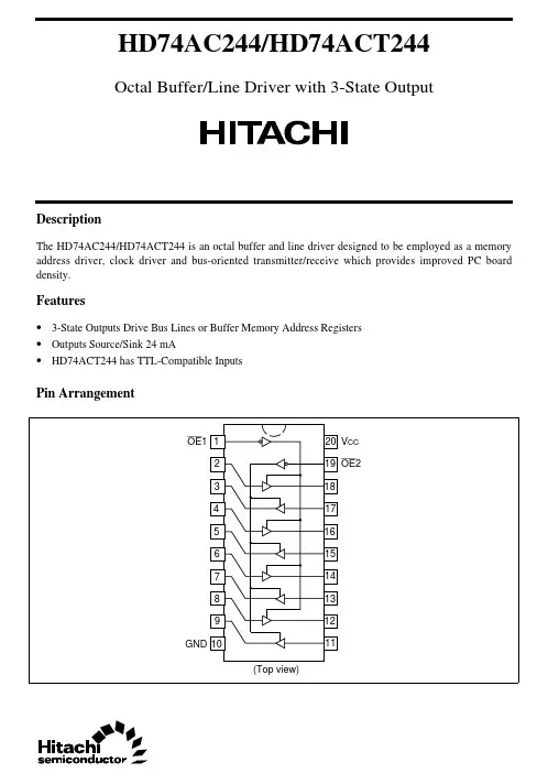
HD74AC244/HD74ACT244Octal Buffer/Line Driver with 3-State OutputREJ03D0262–0200Z(Previous ADE-205-383 (Z))Rev.2.00Jul.16.2004 DescriptionThe HD74AC244/HD74ACT244 is an octal buffer and line driver designed to be employed as a memory address driver, clock driver and bus-oriented transmitter/receive which provides improved PC board density.Features•3-State Outputs Drive Bus Lines or Buffer Memory Address Registers•Outputs Source/Sink 24 mA•HD74ACT244 has TTL-Compatible Inputs•Ordering Information: Ex. HD74AC244Part Name Package Type Package Code Package Abbreviation Taping Abbreviation (Quantity) HD74AC244P DIP-20 pin DP-20N, -20NEV P—HD74AC244FPEL SOP-20 pin (JEITA)FP-20DAV FP EL (2,000 pcs/reel)HD74AC244RPEL SOP-20 pin (JEDEC)FP-20DBV RP EL (1,000 pcs/reel)HD74AC244TELL TSSOP-20 pin TTP-20DAV T ELL (2,000 pcs/reel)Notes: 1.Please consult the sales office for the above package availability.2.The packages with lead-free pins are distinguished from the conventional products by adding V at the end ofthe package code.Pin ArrangementTruth TablesInputs Outputs (Pins 12, 14, 16, 18)OE 1AYL L L L H H HXZInputs Outputs (Pins 3, 5, 7, 9)OE 2AYL L L L H H H XZH :High Voltage Level L :Low Voltage Level X :ImmaterialZ:High ImpedanceAbsolute Maximum RatingsItemSymbol RatingsUnit Condition Supply voltageV CC –0.5 to 7V –20mA V I = –0.5V DC input diode current I IK 20mA V I = Vcc+0.5V DC input voltage V I –0.5 to Vcc+0.5V –50mA V O = –0.5V DC output diode current I OK 50mA V O = Vcc+0.5VDC output voltageV O –0.5 to Vcc+0.5V DC output source or sink current I O±50mA DC V CC or ground current per output pin I CC , I GND ±50mA Storage temperatureTstg–65 to +150°CRecommended Operating Conditions: HD74AC244ItemSymbol RatingsUnitConditionSupply voltageV CC 2 to 6V Input and Output voltage V I , V O 0 to V CC V Operating temperature Ta –40 to +85°C V CC = 3.0V V CC = 4.5 V Input rise and fall time (except Schmitt inputs)V IN 30% to 70% V CCtr, tf8ns/VV CC = 5.5 V+85°C bol (V)min.typ.max.min.max.3.0 2.1 1.5— 2.1—4.5 3.15 2.25— 3.15—V IH5.53.85 2.75— 3.85—V OUT = 0.1 V or V CC –0.1 V3.0— 1.500.9—0.94.5— 2.25 1.35— 1.35Input Voltage V IL5.5— 2.75 1.65— 1.65VV OUT = 0.1 V or V CC –0.1 V3.0 2.9 2.99— 2.9—4.5 4.4 4.49— 4.4—5.5 5.4 5.49— 5.4—V IN = V IL or V IH I OUT = –50 µA 3.0 2.58—— 2.48—I OH = –12 mA 4.53.94—— 3.80—I OH = –24 mA V OH5.5 4.94—— 4.80—V IN = V IL or V IHI OH = –24 mA3.0—0.0020.1—0.14.5—0.0010.1—0.15.5—0.0010.1—0.1V IN = V IL or V IH I OUT = 50 µA 3.0——0.32—0.37I OL = 12 mA 4.5——0.32—0.37I OL = 24 mA Output voltageV OL5.5——0.32—0.37VV IN = V IL or V IHI OL = 24 mAInput leakage current I IN 5.5——±0.1—±1.0µA V IN = V CC or GND 3 State currentI OZ5.5——±0.5—±5.0µA V IN(OE) = V IL , V IH V IN = V CC or GND V OUT = V CC or GND I OLD 5.5———86—mA V OLD = 1.1 V Dynamic output current *I OHD 5.5———–75—mA V OHD = 3.85 VQuiescent supply currentI CC5.5——8.0—80µAV IN = V CC or ground*Maximum test duration 2.0 ms, one output loaded at a time.Recommended Operating Conditions: HD74ACT244ItemSymbol RatingsUnitConditionSupply voltageV CC 2 to 6V Input and output voltage V I , V O 0 to V CC V Operating temperature Ta –40 to +85°C Input rise and fall time (except Schmitt inputs)V IN 0.8 to 2.0 Vtr, tf8ns/VV CC = 4.5V V CC = 5.5V+85°C bol (V)min.typ.max.min.max.4.5 2.0 1.5— 2.0—V IH 5.5 2.0 1.5— 2.0—V OUT = 0.1 V or V CC –0.1 V 4.5— 1.50.8—0.8Input voltage V IL5.5— 1.50.8—0.8VV OUT = 0.1 V or V CC –0.1 V 4.5 4.4 4.49— 4.4—5.5 5.4 5.49— 5.4—V IN = V IL or V IH I OUT = –50 µA 4.53.94—— 3.80—I OH = –24 mA V OH5.5 4.94—— 4.80—V IN = V ILI OH = –24 mA4.5—0.0010.1—0.15.5—0.0010.1—0.1V IN = V IL or V IH I OUT = 50 µA 4.5——0.32—0.37I OL = 24 mA Output voltageV OL5.5——0.32—0.37V V IN = V ILI OL = 24 mA Input current I IN 5.5——±0.1—±1.0µA V IN = V CC or GND 3 State current I OZ 5.5——±0.5—±5.0µA V IN = V IL , V IHV OUT = V CC or GND I CC /input current I CCT 5.5—0.6—— 1.5mA V IN = V CC –2.1 V I OLD 5.5———86—mA V OLD = 1.1 V Dynamic output current *I OHD 5.5———–75—mA V OHD = 3.85 V Quiescent supply currentI CC5.5——8.0—80µA V IN = V CC or ground*Maximum test duration 2.0 ms, one output loaded at a time.AC Characteristics: HD74AC244Ta = +25°C C L = 50 pF Ta = –40°C to +85°CC L = 50 pF ItemSymbol V CC (V)*1Min Typ Max Min Max UnitPropagation delay t PLH 3.3 1.0 6.59.0 1.010.0ns Data to output 5.0 1.0 5.07.0 1.07.5Propagation delay t PHL 3.3 1.0 6.59.0 1.010.0ns Data to output 5.0 1.0 5.07.0 1.07.5Output enable time t ZH 3.3 1.0 6.010.5 1.011.0ns 5.0 1.0 5.07.0 1.08.0Output enable time t ZL 3.3 1.07.510.0 1.011.0ns 5.0 1.0 5.58.0 1.08.5Output disable time t HZ 3.3 1.07.010.0 1.010.5ns 5.0 1.0 6.59.0 1.09.5Output disable time t LZ3.3 1.07.510.5 1.011.5ns5.01.06.59.01.09.5Note:1.Voltage Range 3.3 is 3.3 V ± 0.3 VVoltage Range 5.0 is 5.0 V ± 0.5 VTa = +25°CCL = 50 pFTa = –40°C to +85°CCL= 50 pFItem Symbol VCC(V)*1Min Typ Max Min Max UnitPropagation delay Data to output tPLH5.0 1.06.59.0 1.010.0nsPropagation delay Data to output tPHL5.0 1.07.09.0 1.010.0nsOutput enable time tZH5.0 1.06.08.5 1.09.5nsOutput enable time tZL5.0 1.07.09.5 1.010.5nsOutput disable time tHZ5.0 1.07.09.5 1.010.5nsOutput disable time tLZ5.0 1.07.510.0 1.010.5ns Note: 1.Voltage Range 5.0 is 5.0 V ± 0.5 VCapacitanceItem Symbol Typ Unit ConditionInput capacitance CIN 4.5pF VCC= 5.5 VPower dissipation capacitance CPD 45.0pF VCC= 5.0 VPackage Dimensions RENESAS SALES OFFICESRenesas Technology America, Inc.450 Holger Way, San Jose, CA 95134-1368, U.S.ATel: <1> (408) 382-7500 Fax: <1> (408) 382-7501Renesas Technology Europe Limited.Dukes Meadow, Millboard Road, Bourne End, Buckinghamshire, SL8 5FH, United KingdomTel: <44> (1628) 585 100, Fax: <44> (1628) 585 900Renesas Technology Europe GmbHDornacher Str. 3, D-85622 Feldkirchen, GermanyTel: <49> (89) 380 70 0, Fax: <49> (89) 929 30 11Renesas Technology Hong Kong Ltd.7/F., North Tower, World Finance Centre, Harbour City, Canton Road, Hong KongTel: <852> 2265-6688, Fax: <852> 2375-6836Renesas Technology Taiwan Co., Ltd.FL 10, #99, Fu-Hsing N. Rd., Taipei, TaiwanTel: <886> (2) 2715-2888, Fax: <886> (2) 2713-2999Renesas Technology (Shanghai) Co., Ltd.26/F., Ruijin Building, No.205 Maoming Road (S), Shanghai 200020, ChinaTel: <86> (21) 6472-1001, Fax: <86> (21) 6415-2952Renesas Technology Singapore Pte. Ltd.1, Harbour Front Avenue, #06-10, Keppel Bay Tower, Singapore 098632Tel: <65> 6213-0200, Fax: <65> 6278-8001© 2004. Renesas Technology Corp., All rights reserved. Printed in Japan.Colophon .1.0。