HD74HCT244FPEL中文资料
- 格式:pdf
- 大小:105.13 KB
- 文档页数:7
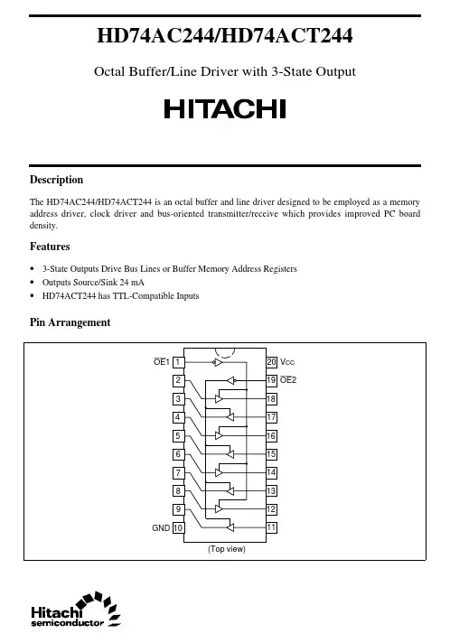
HD74HCT244Octal Buffers/Line Drivers/Line Receivers(with inverted 3-state outputs)REJ03D0664–0200(Previous ADE-205-553)Rev.2.00Mar 30, 2006 DescriptionThe HD74HCT244 is a non-inverting buffer and has two active low enable (1G and 2G). Each enable independently controls 4 buffers.This device does not have schmitt trigger inputs.Features• LSTTL Output Logic Level Compatibility as well as CMOS Output Compatibility• High Speed Operation: t pd (A to Y) = 10 ns typ (C L = 50 pF)• High Output Current: Fanout of 15 LSTTL Loads• Wide Operating Voltage: V CC = 4.5 to 5.5 V• Low Input Current: 1 µA max• Low Quiescent Supply Current: I CC (static) = 4 µA max (Ta = 25°C)• Ordering InformationPart Name Package TypePackage Code(Previous Code)PackageAbbreviationTaping Abbreviation(Quantity)HD74HCT244P DILP-20pin PRDP0020AC-B(DP-20NEV)P —HD74HCT244FPEL SOP-20 pin (JEITA) PRSP0020DD-B(FP-20DAV)FP EL (2,000 pcs/reel)HD74HCT244RPEL SOP-20 pin (JEDEC) PRSP0020DC-A(FP-20DBV)RP EL (1,000 pcs/reel)HD74HCT244TELL TSSOP-20pin PTSP0020JB-A(TTP-20DAV)T ELL (2,000 pcs/reel)Note: Please consult the sales office for the above package availability.Function TableInputs OutputG A YH X ZL H HL L LH : high levelL : low levelX : irrelevantZ : off (high-impedance) state of a 3-state outputPin ArrangementLogic DiagramAbsolute Maximum RatingsUnit Item SymbolRatingsSupply voltage range V CC–0.5 to 7.0 VInput / Output voltage V IN, V OUT–0.5 to V CC +0.5 VInput / Output diode current I IK, I OK±20 mA Output current I O±35 mAV CC, GND current I CC or I GND±75 mAmW Power dissipation P T 500Storage temperature Tstg –65 to +150 °CNote: The absolute maximum ratings are values, which must not individually be exceeded, and furthermore, no two of which may be realized at the same time.Recommended Operating ConditionsItem Symbol Ratings Unit ConditionsSupply voltage V CC 4.5 to 5.5 V Input / Output voltage V IN , V OUT 0 to V CC V Operating temperature Ta –40 to 85 °CInput rise / fall time *1t r , t f 0 to 500 ns V CC = 4.5 V Notes: 1. This item guarantees maximum limit when one input switches. Waveform: Refer to test circuit of switching characteristics.Electrical CharacteristicsTa = 25°C Ta = –40 to+85°CItem Symbol V CC (V)Min Typ Max Min MaxUnit Test ConditionsV IH4.5 to5.5 2.0 — — 2.0 — V Input voltage V IL 4.5 to 5.5 — — 0.8 — 0.8 V4.5 4.4 — — 4.4 — I OH = –20 µA V OH 4.5 4.18 — — 4.13 — V Vin = V IH or V IL I OH = –6 mA 4.5 — — 0.1 — 0.1 I OL = 20 µA Output voltageV OL4.5 — — 0.26 — 0.33 V Vin = V IH or V IL I OL = 6 mAOff-state output currentI OZ 5.5— — ±0.5 — ±5.0 µAVin = V IH or V IL ,Vout = V CC or GND Input currentIin 5.5 — — ±0.1 — ±1.0 µAVin = V CC or GNDQuiescent current I CC 5.5 — — 4.0 — 40 µAVin = V CC or GND, Iout = 0 µASwitching Characteristics(C L = 50 pF, Input t r = t f = 6 ns)Ta = 25°C Ta = –40 to +85°CItem Symbol V CC (V) Min Typ Max Min MaxUnit TestConditionst PHL 4.5 — 11 20 — 25 Propagation delay time t PLH 4.5 — 9 20 — 25nst ZL 4.5 — 13 30 — 38 Output enable time t ZH 4.5 — 12 30 — 38nst LZ 4.5 — 14 30 — 38 Output disable time t HZ 4.5 — 17 30 — 38nsOutput rise/fall time t TLH / t THL 4.5 — 4 12 — 15 ns Input capacitance Cin — — 5 10 — 10 pFTest CircuitWaveformsPackage Dimensions RENESAS SALES OFFICESRefer to "/en/network" for the latest and detailed information.Renesas Technology America, Inc.450 Holger Way, San Jose, CA 95134-1368, U.S.ATel: <1> (408) 382-7500, Fax: <1> (408) 382-7501Renesas Technology Europe LimitedDukes Meadow, Millboard Road, Bourne End, Buckinghamshire, SL8 5FH, U.K.Tel: <44> (1628) 585-100, Fax: <44> (1628) 585-900Renesas Technology (Shanghai) Co., Ltd.Unit 204, 205, AZIACenter, No.1233 Lujiazui Ring Rd, Pudong District, Shanghai, China 200120Tel: <86> (21) 5877-1818, Fax: <86> (21) 6887-7898Renesas Technology Hong Kong Ltd.7th Floor, North Tower, World Finance Centre, Harbour City, 1 Canton Road, Tsimshatsui, Kowloon, Hong KongTel: <852> 2265-6688, Fax: <852> 2730-6071Renesas Technology Taiwan Co., Ltd.10th Floor, No.99, Fushing North Road, Taipei, TaiwanTel: <886> (2) 2715-2888, Fax: <886> (2) 2713-2999Renesas Technology Singapore Pte. Ltd.1 Harbour Front Avenue, #06-10, Keppel Bay Tower, Singapore 098632Tel: <65> 6213-0200, Fax: <65> 6278-8001Renesas Technology Korea Co., Ltd.Kukje Center Bldg. 18th Fl., 191, 2-ka, Hangang-ro, Yongsan-ku, Seoul 140-702, KoreaTel: <82> (2) 796-3115, Fax: <82> (2) 796-2145Renesas Technology Malaysia Sdn. BhdUnit 906, Block B, Menara Amcorp, Amcorp Trade Centre, No.18, Jalan Persiaran Barat, 46050 Petaling Jaya, Selangor Darul Ehsan, MalaysiaTel: <603> 7955-9390, Fax: <603> 7955-9510© 2006. Renesas Technology Corp., All rights reserved. Printed in Japan.。