new phosphor for white LEDs_ materials design concepts
- 格式:pdf
- 大小:699.57 KB
- 文档页数:11
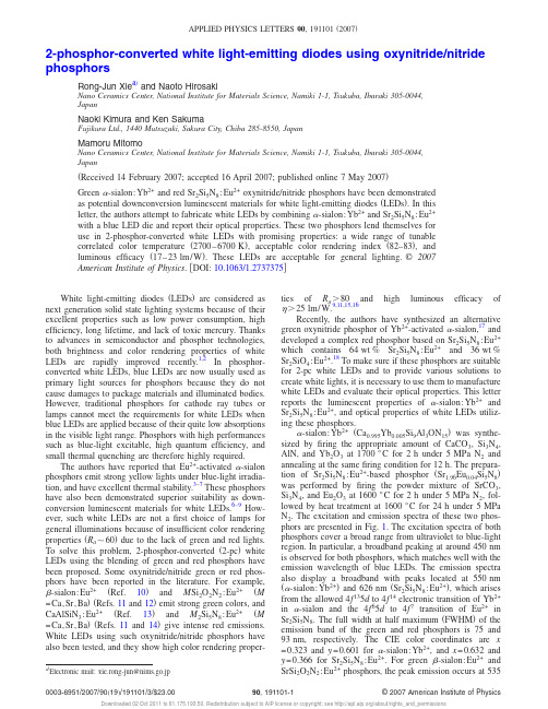
2-phosphor-converted white light-emitting diodes using oxynitride/nitride phosphorsRong-Jun Xie a͒and Naoto HirosakiNano Ceramics Center,National Institute for Materials Science,Namiki1-1,Tsukuba,Ibaraki305-0044,JapanNaoki Kimura and Ken SakumaFujikura Ltd.,1440Mutsuzaki,Sakura City,Chiba285-8550,JapanMamoru MitomoNano Ceramics Center,National Institute for Materials Science,Namiki1-1,Tsukuba,Ibaraki305-0044,Japan͑Received14February2007;accepted16April2007;published online7May2007͒Green␣-sialon:Yb2+and red Sr2Si5N8:Eu2+oxynitride/nitride phosphors have been demonstratedas potential downconversion luminescent materials for white light-emitting diodes͑LEDs͒.In thisletter,the authors attempt to fabricate white LEDs by combining␣-sialon:Yb2+and Sr2Si5N8:Eu2+with a blue LED die and report their optical properties.These two phosphors lend themselves foruse in2-phosphor-converted white LEDs with promising properties:a wide range of tunablecorrelated color temperature͑2700–6700K͒,acceptable color rendering index͑82–83͒,andluminous efficacy͑17–23lm/W͒.These LEDs are acceptable for general lighting.©2007American Institute of Physics.͓DOI:10.1063/1.2737375͔White light-emitting diodes͑LEDs͒are considered as next generation solid state lighting systems because of their excellent properties such as low power consumption,high efficiency,long lifetime,and lack of toxic mercury.Thanks to advances in semiconductor and phosphor technologies, both brightness and color rendering properties of white LEDs are rapidly improved recently.1,2In phosphor-converted white LEDs,blue LEDs are now usually used as primary light sources for phosphors because they do notcause damages to package materials and illuminated bodies.However,traditional phosphors for cathode ray tubes orlamps cannot meet the requirements for white LEDs whenblue LEDs are applied because of their quite low absorptionsin the visible light range.Phosphors with high performancessuch as blue-light excitable,high quantum efficiency,andsmall thermal quenching are therefore highly required.The authors have reported that Eu2+-activated␣-sialon phosphors emit strong yellow lights under blue-light irradia-tion,and have excellent thermal stability.3–7These phosphorshave also been demonstrated superior suitability as down-conversion luminescent materials for white LEDs.6–9How-ever,such white LEDs are not afirst choice of lamps forgeneral illuminations because of insufficient color renderingproperties͑R aϳ60͒due to the lack of green and red lights. To solve this problem,2-phosphor-converted͑2-pc͒whiteLEDs using the blending of green and red phosphors havebeen proposed.Some oxynitride/nitride green or red phos-phors have been reported in the literature.For example,-sialon:Eu2+͑Ref.10͒and M Si2O2N2:Eu2+͑M =Ca,Sr,Ba͒͑Refs.11and12͒emit strong green colors,and CaAlSiN3:Eu2+͑Ref.13͒and M2Si5N8:Eu2+͑M =Ca,Sr,Ba͒͑Refs.11and14͒give intense red emissions. White LEDs using such oxynitride/nitride phosphors have also been tested,and they show high color rendering proper-ties of R aϾ80and high luminous efficacy of Ͼ25lm/W.9,11,15,16Recently,the authors have synthesized an alternative green oxynitride phosphor of Yb2+-activated␣-sialon,17and developed a complex red phosphor based on Sr2Si5N8:Eu2+ which contains64wt%Sr2Si5N8:Eu2+and36wt% Sr2SiO4:Eu2+.18To make sure if these phosphors are suitable for2-pc white LEDs and to provide various solutions to create white lights,it is necessary to use them to manufacture white LEDs and evaluate their optical properties.This letter reports the luminescent properties of␣-sialon:Yb2+and Sr2Si5N8:Eu2+,and optical properties of white LEDs utiliz-ing these phosphors.␣-sialon:Yb2+͑Ca0.995Yb0.005Si9Al3ON15͒was synthe-sized byfiring the appropriate amount of CaCO3,Si3N4, AlN,and Yb2O3at1700°C for2h under5MPa N2and annealing at the samefiring condition for12h.The prepara-tion of Sr2Si5N8:Eu2+-based phosphor͑Sr1.96Eu0.04Si5N8͒was performed byfiring the powder mixture of SrCO3, Si3N4,and Eu2O3at1600°C for2h under5MPa N2,fol-lowed by heat treatment at1600°C for24h under5MPa N2.The excitation and emission spectra of these two phos-phors are presented in Fig.1.The excitation spectra of both phosphors cover a broad range from ultraviolet to blue-light region.In particular,a broadband peaking at around450nm is observed for both phosphors,which matches well with the emission wavelength of blue LEDs.The emission spectra also display a broadband with peaks located at550nm ͑␣-sialon:Yb2+͒and626nm͑Sr2Si5N8:Eu2+͒,which arises from the allowed4f135d to4f14electronic transition of Yb2+ in␣-sialon and the4f65d to4f7transition of Eu2+in Sr2Si5N8.The full width at half maximum͑FWHM͒of the emission band of the green and red phosphors is75and 93nm,respectively.The CIE color coordinates are x =0.323and y=0.601for␣-sialon:Yb2+,and x=0.632and y=0.366for Sr2Si5N8:Eu2+.For green-sialon:Eu2+and SrSi2O2N2:Eu2+phosphors,the peak emission occurs at535a͒Electronic mail:xie.rong-jun@nims.go.jpAPPLIED PHYSICS LETTERS90,191101͑2007͒0003-6951/2007/90͑19͒/191101/3/$23.00©2007American Institute of Physics90,191101-1and 538nm,respectively.10,11The FWHM of ␣-sialon:Yb 2+is larger than that of -sialon:Eu 2+͑55nm ͒and comparable to that of SrSi 2O 2N 2:Eu 2+͑78nm ͒.The internal quantum efficiency,measured under 450nm excitation at room tem-perature,is 57%and 79%for ␣-sialon:Yb 2+and Sr 2Si 5N 8:Eu 2+,respectively.Thermal quenching is one of the important technological parameters for phosphors used in white LEDs.The temperature-dependent luminescent properties were mea-sured at temperatures in the range of 22–250°C,and the results are shown in Fig.2.Upon heating,the decrease in emission intensity and the broadening of FWHM is apparent,and these can be explained by the thermal quenching at con-figurational coordinate diagram.19,20With increasing tem-perature,the nonradiative transition probability by thermal activation and release of the luminescent center through the crossing point between the excited state and the ground state increases,which quenches the luminescence.The electron-phonon interaction is enhanced at high temperature as a re-sult of increased population density of phonon,which broad-ens FWHM.The integral emission intensity,proportional to the quantum efficiency,decreases slightly less than the peak intensity.The thermal quenching temperature T 50defined as the temperature at which the emission intensity is 50%of its original value,is 234°C for ␣-sialon:Yb 2+and 335°C for Sr 2Si 5N 8:Eu 2+.At 150°C,the emission intensity of ␣-sialon:Yb 2+and Sr 2Si 5N 8:Eu 2+is about 74%and 86%of that measured at room temperature,respectively.In addition,a slight blueshift of the emission band is observed for both phosphors as the temperature increases.It can be explained by thermally active phonon-assisted excitation from lower-energy sublevel to higher-energy sublevel in excited states of Eu 2+.19To better understand the temperature dependence of photoluminescence and to determine the activation energyfor thermal quenching,the Arrhenius equation was fitted to the thermal quenching data,21I ͑T ͒=I 01+c expͩ−EkTͪ,͑1͒where I 0is the initial intensity,I ͑T ͒is the intensity at a given temperature T ,c is a constant,E is the activation energy for thermal quenching,and k is Boltzmann’s constant.Figure 3plots ln ͓͑I 0/I ͒−1͔vs 1/͑kT ͒and gives a straight line up to T =250°C.The best fit following Eq.͑1͒gives a comparable activation energy E of 0.23eV for ␣-sialon:Yb 2+and 0.20eV for Sr 2Si 5N 8:Eu 2+.Five types of white LEDs,class D ͑daylight ͒,class N ͑neutral white ͒,class W ͑white ͒,class WW ͑warm white ͒,and class L ͑incandescent light bulb ͒,with the surface mount device ͑SMD ͒,were prepared by combining ␣-sialon:Yb 2+and Sr 2Si 5N 8:Eu 2+with a blue LED die.The blue LED die was fixed in a SMD package and connected to electrodes.The phosphor blend was made by dispersing two phosphors with varying ratios in a transparent silicone resin,and white LEDs were then fabricated by coating the LED die withtheFIG. 1.Excitation ͑a ͒and emission ͑b ͒spectra of ␣-sialon:Yb 2+and Sr 2Si 5N 8:Eu 2+.ex =450nm for emission spectra,and em =550nm and em =626nm for excitation spectra of ␣-sialon:Yb 2+and Sr 2Si 5N 8:Eu 2+,respectively.The emission spectrum of a blue LED die is also included in both ͑a ͒and ͑b ͒.FIG.2.Temperature dependence of emission spectra of ͑a ͒␣-sialon:Yb 2+and ͑b ͒Sr 2Si 5N 8:Eu 2+.The insets show the temperature dependence of peak intensity and integral intensity of bothphosphors.FIG.3.Activation energy for thermal quenching of ␣-sialon:Yb 2+and Sr 2Si 5N 8:Eu 2+.resin.The optical properties of white LEDs were measured under a forward-bias current of 20mA at room temperature.Table I summarizes the optical properties of these lamps.Note that various types of white LEDs with adjustable cor-related color temperatures ͑CCTs ͒can be simply made by optimizing the blending ratio of green and red phosphors.Figure 4presents the emission spectra of various types of white LEDs.As seen,the color rendering index of these white LEDs achieves R a =82–83.This value is much higher than that of white LEDs using a single ␣-sialon:Eu 2+yellow phosphor,6–9and comparable to that of white LEDs using three phosphors consisting of -sialon:Eu 2+,␣-sialon:Eu 2+,and CaAlSiN 3:Eu 2+͑R a =81–88͒.9This value would be fur-ther improved by adding a blue-green phosphor such as BaSi 2O 2N 2:Eu 2+͑em =500nm ͒.15The luminous efficacy of the class L white LED is 17lm/W,which is lower than that of the same type of white LED using -sialon:Eu 2+,␣-sialon:Eu 2+,and CaAlSiN 3:Eu 2+͑25lm/W ͒.9The reason for this low value is mainly attributable to the relatively low emission intensity of the ␣-sialon:Yb 2+green phosphor ͑compared to -sialon:Eu 2+͒.Other types of our white LEDs reach 20–23lm/W,which is at the same level reported in Ref.9.We believe that the luminous efficacy of our white LEDs can be significantly enhanced by optimizing the mor-phology and particle size of both green and red phosphors.In summary,green ␣-sialon:Yb 2+and red Sr 2Si 5N 8:Eu 2+oxynitride/nitride phosphors have demon-strated their suitability for 2-pc white LEDs.The white LEDshave shown good optical properties with a broad range of white lights with tunable color temperature as well as accept-able color rendering properties for general illuminations.Further studies to improve the performances of white LEDs by optimizing the luminescent properties of phosphors are underway.1Y .Narukawa,S.Nagahama,H.Tamaki,and T.Mukai,Oyo Butsuri 74,1423͑2005͒.2Press released by Cree,Inc.on Oct.9,2006͑/presee ͒.3R.-J.Xie,M.Mitomo,K.Uheda,F.-F.Xu,and Y .Akimune,J.Am.Ce-ram.Soc.85,1229͑2002͒.4R.-J.Xie,N.Hirosaki,M.Mitomo,Y .Yamamoto,T.Suehiro,and K.Sakuma,J.Phys.Chem.B 108,12708͑2004͒.5R.-J.Xie,N.Hirosaki,K.Sakuma,Y .Yamamoto,and M.Mitomo,Appl.Phys.Lett.84,5404͑2004͒.6R.-J.Xie,N.Hirosaki,M.Mitomo,K.Takahashi,and K.Sakuma,Appl.Phys.Lett.88,101104͑2006͒.7R.-J.Xie,N.Hirosaki,M.Mitomo,K.Sakuma,and N.Kimura,Appl.Phys.Lett.89,241103͑2006͒.8K.Sakuma,K.Omichi,N.Kimura,M.Ohashi,D.Tanaka,N.Hirosaki,Y .Yamamoto,R.-J.Xie,and T.Suehiro,Opt.Lett.29,2001͑2004͒.9K.Sakuma,N.Hirosaki,N.Kimura,M.Ohashi,R.-J.Xie,Y .Yamamoto,T.Suehiro,K.Asano,and D.Tanaka,IEICE Trans.Electron.E88-C ,2057͑2005͒.10N.Hirosaki,R.-J.Xie,K.Kimoto,T.Sekiguchi,Y .Yamamoto,T.Suehiro,and M.Mitomo,Appl.Phys.Lett.86,211905͑2005͒.11R.Mueller-Mach,G.Mueller,M.R.Krames,H.A.Höppe,F.Stadler,W.Schnick,T.Juestel,and P.Schmidt,Phys.Status Solidi A 202,1727͑2005͒.12Y .Q.Li,A.C.A.Delsing,G.de With,and H.T.Hintzen,Chem.Mater.17,3242͑2005͒.13K.Uheda,N.Hirosaki,Y .Yamamoto,A.Naito,T.Nakajima,and H.Yamamoto,Electrochem.Solid-State Lett.9,H22͑2006͒.14Y .Q.Li,G.de With,and H.T.Hintzen,J.Lumin.116,107͑2006͒.15N.Kimura,K.Sakuma,S.Hirafune,K.Asano,N.Hirosaki,and R.-J.Xie,Appl.Phys.Lett.90,051109͑2007͒.16C.-C.Yang,C.-M.Lin,Y .-J.Chen,Y .-T.Wu,S.-R.Chuang,R.-S.Liu,and S.-F.Hu,Appl.Phys.Lett.90,123503͑2007͒.17R.-J.Xie,N.Hirosaki,M.Mitomo,K.Uheda,T.Suehiro,X.Xu,Y .Yamamoto,and T.Sekiguchi,J.Phys.Chem.B 109,9490͑2005͒.18R.-J.Xie,N.Hirosaki,T.Suehiro,F.-F.Xu,and M.Mitomo,Chem.Mater.18,5578͑2006͒.19S.Shionoya and W.M.Yen,Phosphor Handbook ,Laser &Optical Sci-ence &Technology Series ͑CRC,New York,1998͒,pp.65–220.20J.S.Kim,Y .H.Park,S.M.Kim,J.C.Choi,and H.L.Park,Solid State Commun.133,445͑2005͒.21S.Bhushan and M.V .Chukichev,J.Mater.Sci.Lett.9,319͑1988͒.TABLE I.Optical properties of five types of 2-pc-white LEDs.ClassL WW W N D CCT ͑K ͒27443590427050336508CIE x 0.4610.4020.3720.3440.313CIE y 0.4190.3930.3820.3460.330R a8383838382Luminous efficacy ͑lm/W ͒1720212223FIG.4.͑Color ͒Emission spectra of 2-pc-white LEDs,measured under a forward-bias current of 20mA at room temperature.。
Luminescence Properties and Energy-Transfer Behavior of a Novel and Color-Tunable LaMgAl11O19:Tm3+,Dy3+Phosphor for White Light-Emitting Diodes Xin Min,Minghao Fang,†Zhaohui Huang,Yan’gai Liu,Chao Tang,and Xiaowen Wu Beijing Key Laboratory of Materials Utilization of Nonmetallic Minerals and Solid Wastes,National Laboratory of Mineral Materials,School of Materials Science and Technology,China University of Geosciences(Beijing),Beijing100083,ChinaNovel LaMgAl11O19:Tm3+,Dy3+phosphors were prepared utilizing a high-temperature solid-state reaction method.The phase formation,luminescence properties,energy-transfer mechanism from the Tm3+to the Dy3+ions,the thermal sta-bility,and CIE coordinates were investigated.When excited at 359nm,the LaMgAl11O19:x Tm3+phosphors exhibit strong blue emission bands at455nm.After codoping with Dy3+and excitation at359nm,the LaMgAl11O19:0.03Tm3+,y Dy3+ phosphors emitted white light consisting of the characteristic emission peaks of Tm3+and Dy3+.The Dy3+emission inten-sity increased with the Dy3+concentration due to the energy transfer from Tm3+to Dy3+,and concentration quenching due to the high Dy3+doping concentration(y=0.1mol)did not occur.The calculation of the CIE coordinates of the LaM-gAl11O19:Tm3+,y Dy3+phosphors revealed the tunability of the emission color from blue to bluish-white and to white by changing the excitation wavelength and the doping concentra-tion.An energy transfer from Tm3+to Dy3+by dipole–dipole interaction was confirmed by the decay curve,lifetime,and energy-transfer efficiency measurements.When excited at 359nm,the LaMgAl11O19:Tm3+,Dy3+phosphor also showed good thermal stability,suggesting that it can be used in white LEDs excited by a GaN-based ultraviolet LED.I.IntroductionW HITE light-emitting diodes(w-LEDs)was widely considered as fourth generation solid-state light sources due to their high luminous efficiency,long lifetime,good reli-ability,low-energy consumption,and low environmental impact.1–3Thefirst generation of w-LEDs simply consisted of three individual LED chips,that is,a blue,green,and red light-emitting LED,which are easy to produce,but are also regarded as possessing a limited usability and application potential because of several disadvantages,for example,a fabrication high cost,the differences in drive voltage,inferior thermal properties,and susceptibility to degradation.4A second approach to obtain white light is based on the combination of a blue light-emitting GaN chip with yellow light-emitting phosphors(e.g.,Y3Al5O12:Ce3+).5,6However, the resulting white light shows a poor color rendering index, chromatic aberration,and poor white light-emitting perfor-mance,due to the lack of red components and the difference in degradation behavior between the GaN chip and phos-phors.7,8A third category of white LEDs contains blue,green,and red light-emitting phosphors which are excited by an ultravi-olet(UV)LED chip in the wavelength range of340to 380nm.9However,the reabsorption among the phosphors results in a low luminous efficiency,and the advanced coat-ing techniques required for their fabrication and their low chemical stability against humidity restricts their application potential.10,11Compared with existing phosphors used in w-LEDs, these approaches do not meet the optimum requirements of w-LEDs.Thus,current studies focus on single-phase white light-emitting phosphors excited with an UV LED,which might be able to overcome the shortcomings described above and offer additional advantages such as a high luminous effi-ciency,excellent color rendering indexes,a small color aber-ration,good stability,and a simple fabrication process.12–14 As reported in literature,these single-phase white light-emit-ting phosphors are frequently codoped with a sensitizer and an activator.15–18So far,the fabrication of Sr3Y(PO4)3:Eu2+, Mn2+,15Ba2Ca(BO3)2:Ce3+,Mn2+,16Ca2Al2SiO7:Ce3+, Tb3+,17and Sr3B2O6:Ce3+,Eu2+18single-phase white light-emitting phosphors has been reported.However,these phos-phors were synthesized in a reducing atmosphere,which may also limit further application due to the complex preparation process.Thus,a novel single-component white light-emitting phosphor which can be synthesized under ambient atmo-spheric conditions would be highly desirable.Therefore,in this study,a white light-emitting phosphor activated with Dy3+ions has been prepared under ambient atmospheric conditions.Under excitation of a GaN-based UV LED chip,the phosphor mainly exhibits two emission bands in the blue and yellow regions of the spectra,due to 4F9/2?6H13/2and4F9/2?6H15/2transitions,respectively.19,20 However,the quality of the white light is unsatisfactory,as the color coordinates of the Dy3+phosphor are a quite far away from the equal energy point.The color coordinates can be readjusted by codoping red light-emitting ions if the blue emission is stronger than the yellow light emission.On the other hand,if the yellow light emission is stronger than the blue light emission,blue light-emitting ions can be added to modify the color coordinates.21–23Hexaaluminate materials,for example,lanthanum magne-sium hexaaluminate,LaMgAl11O19,are widely considered as host material for phosphors because of their high physical and chemical stability and low fabrication cost.24,25Previ-ously published results19indicate that the yellow emission of Dy3+-activated LaMgAl11O19phosphors is stronger than the blue emission.On the other hand,Tm3+ions are known to emit strong blue light in a LaMgAl11O19host matrix.There-fore,Tm3+ions were introduced into the Dy3+-activated LaMgAl11O19phosphors to optimize the color coordinates.A detail luminescent characterization of LaMgAl11O19phos-phors codoped with both Tm3+and Dy3+has not been reported so far,and the energy transfer(ET)between the Tm3+and Dy3+ions was also rarely investigated.In this study,the LaMgAl11O19:Tm3+,Dy3+phosphors were syn-thesized utilizing a high-temperature solid-state method in an ambient atmosphere.The phase structure and luminescence properties of the resulting materials were investigated inB.Dunn—contributing editorManuscript No.35312.Received July16,2014;approved October23,2014.†Author to whom correspondence should be addressed.e-mail:fmh@1J.Am.Ceram.Soc.,1–7(2014)DOI:10.1111/jace.13346©2014The American Ceramic SocietyJ ournaldetail.The thermal stability of the LaMgAl11O19:Tm3+,Dy3+phosphor was obtained by analyzing the temperature-dependent emission spectra.In addition,the CIE chromatic-ity coordinates of the phosphor are presented.II.Experimental ProcedureFor this study,La1Àx MgAl11O19:x Tm3+(x=0.01,0.03,0.05,0.08),La0.9MgAl11O19:0.1Dy3+,andLa0.9Ày MgAl11O19:0.03Tm3+,y Dy3+(y=0.01,0.03,0.05, 0.1,0.15)phosphors were synthesized utilizing the high-tem-perature solid-state reaction method,with Al(OH)3(99.9%),Mg(OH)2(99.9%),La2O3(99.9%),Tm2O3(99.9%),andDy2O3(99.9%)used as raw materials.As La2O3powders can rapidly absorb atmospheric water,they were weighedimmediately after an annealing step at1100°C for1h.Stoi-chiometric amounts of these raw materials were well-mixed in an agate mortar for1h.The mixtures were then moldedby uniaxial pressing at15MPa,and then calcined at1600°Cfor4h.Afterward,the sintered samples were allowed to cooldown to room temperature and ground into powders for the subsequent measurements.The crystal structure of the phosphors was investigatedby X-ray diffraction analysis(XRD;D8Advance diffrac-tometer,Bruker Corporation,Karlsruhe,Germany)using Cu K a radiation(k=1.5406 A).The room-temperature photoluminescence excitation(PLE)and emission(PL)spectra were recorded on afluorescence spectrophotometer (F-4600;Hitachi,Tokyo,Japan)equipped with a photo-multiplier tube operating at550V.A150W Xe lamp was used as excitation source.The temperature-dependent emis-sion spectra were also recorded on the same spectropho-tometer which was combined with a computer-controlled heating element.The room-temperature decay curves were obtained by utilizing a spectrofluorometer(TBX-PS;HORIBA Jobin Yvon,Paris,France),with368-nm pulse laser radia-tion used as the excitation source.The CIE coordinates werefinally calculated according to the CIE1931standard colorimetric systems using a self-programmed software tool.III.ResultsThe XRD patterns of the LaMgAl11O19:Tm3+,LaM-gAl11O19:Dy3+,and LaMgAl11O19:Tm3+,Dy3+phosphors are shown in Fig.1.It can be seen that the peak positions are in good agreement with the peak positions on the corre-sponding JCDPS card(no.78-1845),indicating that the absence of impurity phases in the host structure.The latticeparameters of the hexaaluminate structure are as follows: a=b=5.59 A,c=21.97 A,a=b=90°,c=120°, V=594.53 A3.26At 1.03,0.88,and0.91 A for the La3+, Tm3+,and Dy3+ions,respectively,the three ionic radii are very similar.27All these results indicate that the Tm3+and Dy3+ions are replacing the La3+ions on their sites in the LaMgAl11O19lattice without changing the material’s struc-ture.The PLE and PL spectra of the fabricated LaMgAl11O19: x Tm3+(x=0.01,0.03,0.05,0.08)phosphors are shown in Fig.2.The emission spectrum recorded for an excitation wavelength of359nm exhibits a strong emission peak centered at455nm and a weak emission band at515nm, which correspond to the1D2?3F4and1G4?3H6transition, respectively.21–23The excitation spectrum for the455nm light emission consists of a main peak centered at359nm, which is usually attributed to the Tm3+3H6?1D2f–f transition.21–23The emission mechanism for the Tm3+ions in the LaM-gAl11O19samples is presented in the partial energy level dia-gram shown in Fig.7.The inset image in Fig.2shows the emission intensity as a function of the Tm3+ion concentra-tion.The intensityfirstly increases with the Tm3+ions con-centration,reaching a maximum at x=0.03mol,and then decreases due to concentration quenching.The CIE chromaticity coordinates of the LaMgAl11O19:0.03Tm3+ phosphor were calculated to X=0.1579and Y=0.0553,rep-resented by point A in Fig.9.These values are close to the coordinates of the reference illuminants of the National Tele-vision Standard Committee(NTSC:X=0.155,Y=0.070) and the European Broadcasting Union(EBU:X=0.150, Y=0.060),respectively.Figure3shows the PLE and PL spectra obtained for the Dy3+-doped LaMgAl11O19samples.As shown in Fig.3(a), the excitation spectrum monitored at an excitation wave-length of570nm contains a broad absorption band ranging from250to500nm.The excitation peaks centered at275, 294,323,348,363,386,426,452,and472nm are attributed to the transitions from6H15/2to4K11/2,4D7/2,4M17/2,9P7/2, 4P5/2,4I13/2,4G11/2,4I15/2,and4F9/2,respectively.19,20In the emission spectrum obtained for an excitation at348nm,a blue emission peak at475nm,a yellow emission peak at 570nm,and a weak red emission peak at664nm were observed,as shown in Fig.3(b).These characteristic emission peaks correspond to the4F9/2?6H15/2,4F9/2?6H13/2,and 4F9/2?6H11/2transition of Dy3+ions,respectively.19,20The Fig.1.XRD patterns obtained for LaMgAl11O19:0.03Tm3+, LaMgAl11O19:0.1Dy3+,LaMgAl11O19:0.03Tm3+,0.1Dy3+,and the corresponding JCPDS card for LaMgAl11O19.Fig.2.PLE(left)and PL(right)spectra of LaMgAl11O19:x Tm3+. The inset image shows the Tm3+emission intensity of as a function of the Tm3+ion concentration.2Journal of the American Ceramic Society—Min et al.energy level diagram shown in Fig.7also illustrates the luminescence mechanism of the LaMgAl11O19:Dy3+ phosphors.The CIE chromaticity coordinates for the LaM-gAl11O19:0.1Dy3+phosphor excited at348nm is are X=0.3324and Y=0.3665,as shown in Fig.9(point D), which is quite far away from the standard equal energy point for white light(X=0.3333,Y=0.3333).Furthermore,Fig.3(b)also shows that the intensity of the yellow lightemission peak of the LaMgAl11O19:0.1Dy3+phosphor is stronger than the intensity of the blue light emission peak,suggesting that the matrix material should be codoped withblue light-emitting ions to improve the color coordinates.As shown in Fig.4(a),a spectral overlap between theemission spectrum of LaMgAl11O19:0.03Tm3+and the exci-tation spectrum of LaMgAl11O19:0.1Dy3+was found.According to the essential conditions for energy transfer pro-posed by Blasse,28an effective resonance-type energy transferfrom the Tm3+to the Dy3+ions can be expected in theTm3+and Dy3+codoped LaMgAl11O19samples.As shownin Fig.4(b),the PL spectrum of the LaM-gAl11O19:0.03Tm3+,0.1Dy3+phosphor consists of threemain emission bands and two weak emission bands corre-sponding to the1D2?3F4(455nm)and1G4?3H6(515nm) transition of Tm3+ions and the4F9/2?6H15/2(475nm),4F9/ 2?6H13/2(570nm),and4F9/2?6H11/2(664nm)transition of Dy3+ions,suggesting the occurrence of an energy transferfrom the Tm3+to the Dy3+ions as reported in literature.29 The emission spectra of the LaMgAl11O19:0.03Tm3+, y Dy3+(y=0,0.01,0.03,0.05,0.1,0.15)phosphors recorded for an excitation at359nm are shown in Fig.5.All these spectra exhibit the emission bands of both Tm3+and Dy3+ ions,centered at455,475,515,570,and664nm,respec-tively.As illustrated by the inset image in Fig.5,the emis-sion intensity of the Tm3+ions gradually decreases as the Dy3+concentration increases,indicating an energy transfer from Tm3+to Dy3+.Furthermore,the intensity of the emis-sion peaks at475and570nm increases with the concentra-tion of Dy3+ranging from0.01to0.1mol,and then starts to decrease as the Dy3+concentration further increases due to the concentration quenching of the luminescence.In Fig.6,the emission spectra of LaMgAl11O19:0.03Tm3+,y Dy3+(y=0,0.01,0.03,0.05,0.1,0.15)phosphors are pre-sented for an excitation at348nm.The spectrum of LaM-gAl11O19:0.03Tm3+phosphor recorded after excitation at 348nm shows a weak emission peak centered at455nm, which is attributed to the Tm3+ions and caused by the weak absorption.The Tm3+emission intensity obviously decreases as the Dy3+ion concentration increases.Furthermore,the intensity of the emission peaks at475and570nm associated with the Dy3+ions increase with Dy3+ion concentration. These results further indicate an energy transfer from Tm3+ to Dy3+.The energy level diagram shown in Fig.7illustrates the energy-transfer process from the Tm3+to the Dy3+ions.(a)(b)Fig.3.PLE(a)and PL(b)spectra of LaMgAl11O19:0.1Dy3+.(a)(b)Fig.4.(a)Spectral overlap between the PL spectrum of LaMgAl11O19:0.03Tm3+and PLE spectrum of LaMgAl11O19:0.1Dy3+;(b)PL spectra of the LaMgAl11O19:0.03Tm3+,0.1Dy3+phosphor.Phosphors for w-LEDs3When the LaMgAl 11O 19:Tm 3+,Dy 3+phosphor was excited at 359nm,the electrons in the Dy 3+ions in the ground state (6H 15)of were excited to the 4I 15/2state by an energy transfer from the Tm 3+ions,due to the similar energy gap between the 1D 2?3F 4transition (22221cm À1)of the Tm 3+ions and the 6H 15/2?4I 15/2transition (22253cm À1)of the Dy 3+ions.Then,the electrons on the 4I 15/2energy level non-radiatively relax to the 4F 9/2level.The electrons on the 4F 9/2level finally relax to 6H 15/2,6H 13/2,and 6H 11/2levels,resulting in the emission bands located at 475,570,and 664nm,respectively.Concerning the application in high-powder w-LEDs,the thermal stability is one of the crucial properties of the phos-phors.Figure 8shows the emission spectra of the LaM-gAl 11O 19:0.03Tm 3+,0.1Dy 3+phosphor obtained at different temperatures for k ex =359nm.With increasing temperature,the intensity of the emission spectrum gradually decreases.At a temperature of 150°C,the emission intensity had dropped to approx.51%of the intensity measured at room temperature.As shown in the inset image in Fig.8,the Arrhenius fitting curves of the emission intensity of the LaM-gAl 11O 19:0.03Tm 3+,0.1Dy 3+phosphor and the calculated activation energy (M E )for thermal quenching were obtained.The activation energy can be calculated using the following equation 30:I T ¼I 0½1þC exp ðÀD EkT Þ(1)where I T represents the emission intensity of the phosphor at temperatures T ,I 0denotes the intensity at room temperature,C is a constant,and k is the Boltzmann constant (8.62910À5eV).As shown on the inset image,a nonlinear function was fitted to the experimentally obtained ln[(I 0/I T )À1]vs 1/kT data plot,and the activation energy M E was calcu-lated to be 0.56eV.These results indicate that the LaM-gAl 11O 19:Tm 3+,Dy 3+phosphor exhibits a good thermal stability and is therefore suitable for an application in high-power w-LEDs.The calculated CIE chromaticity coordinates of the LaMgAl 11O 19:x Tm 3+,y Dy 3+phosphor are compared in Table I for different excitation wavelengths.The CIE chro-maticity coordinates are also shown in the CIE diagram in Fig.9.Under 359nm excitation,the emission color changes from blue to a bluish-white.For an excitation at 348nm,the color of the emitted light gradually changes to white light.The CIE chromaticity coordinates of the LaM-gAl 11O 19:0.03Tm 3+,0.1Dy 3+and LaMgAl 11O 19:0.03Tm 3+,0.15Dy 3+phosphors excited at 348nm are X =0.2971and Y =0.3281(C4),and X =0.2978and Y =0.3311(C5),Fig.5.PL spectra obtained for LaMgAl 11O 19:0.03Tm 3+,y Dy 3+phosphors with different Dy 3+ion concentrations recorded under excitation at 359nm.The inset image shows the normalized intensity of different emission peaks as a function of the Dy 3+dopingconcentration.Fig.6.PL spectra obtained for LaMgAl 11O 19:0.03Tm 3+,y Dy 3+phosphors with different Dy 3+ion concentrations recorded under excitation at 348nm.Fig.7.Energy level diagram for the Tm 3+and Dy 3+ions in the LaMgAl 11O 19:Tm 3+,Dy 3+phosphors.4Journal of the American Ceramic Society—Min et al.respectively,which are very close to the equal energy point (X =0.3333,Y =0.3333).Consequently,the light emission of LaMgAl 11O 19:Tm 3+,Dy 3+phosphors can be tuned from blue to a bluish-white,and finally to white light by changing the excitation wavelength and the doping concentration of the Dy 3+and Tm 3+ions.IV.DiscussionTo further confirm the energy transfer from the Tm 3+ions to the Dy 3+ions,the luminescence decay curves of Tm 3+were recorded at an excitation wavelength of 368nm,while monitoring at 455nm.As shown in Fig.10,all curves can be described by a single-exponential decay function,and the luminescence lifetimes can be calculated using the following equation:28I ¼I 0expÀt s(2)where I and I 0correspond to the luminescence intensity at time t and the initial time,respectively,and s denotes thelifetimes.Based on these parameters,the lifetimes were calcu-lated to 45.6,40.5,37.3,33.6,19.4,and 12.2l s for LaMgAl 11O 19:0.03Tm 3+,y Dy 3+phosphors with y =0,0.01,0.03,0.05,0.1,and 0.15,respectively.The quenching in life-time of the Tm 3+ions with the increasing Dy 3+ion concen-tration confirms the energy transfer from Tm 3+to Dy 3+.The energy-transfer efficiency (g ET )can be calculated by the following equation:31g ET ¼1Às s s 0(3)where s s is the lifetime of the sensitizer (Tm 3+)in the pres-ence of the activator (Dy 3+),and s 0is the lifetime of the sen-sitizer in the absence of an activator.As shown in the inset table in Fig.10,the energy-transfer efficiency increaseswithFig.8.PL spectra (k ex =359nm)obtained for theLaMgAl 11O 19:0.03Tm 3+,0.1Dy 3+phosphor at different temperatures (from 25°C to 150°C).The inset image shows the Arrhenius fitting curve for the emission intensity of the LaMgAl 11O 19:0.03Tm 3+,0.1Dy 3+phosphor and the calculated activation energy (M E )for thermal quenching.Table parison of the CIE Chromaticity Coordinates (X ,Y )for LaMgAl 11O 19:x Tm 3+,y Dy 3+Phosphors forDifferent Excitation WavelengthsPoint in Fig.9k exC (Tm 3+)(x )C (Dy 3+)(y )CIE coordinatesXYA 359nm0.0300.15790.0553B10.030.010.17220.0845B20.030.030.18790.1154B30.030.050.20100.1412B40.030.10.22420.1866B50.030.150.23830.2182C1348nm0.030.010.23540.2158C20.030.030.26860.2765C30.030.050.28210.3010C40.030.10.29710.3281C50.030.150.29780.3311D00.10.33240.3665Fig.9.The CIE chromaticity coordinates calculated for the LaMgAl 11O 19:Tm 3+,Dy 3+phosphors.Fig.10.Decay curves obtained for Tm 3+in LaMgAl 11O 19:0.03Tm 3+,y Dy 3+phosphor (excited at 368nm,monitored at 455nm).The inset table shows the lifetimes and energy-transfer (ET)efficiency for different Tm 3+ion concentrations.Phosphors for w-LEDs 5the Dy3+concentration,again corroborating the energy transfer from Tm3+to Dy3+.To determine the interaction mechanism for the energy transfer from the Tm3+to the Dy3+ions,Dexter’s energy-transfer formula for multipolar interaction and Reisfeld’s approximation were applied,which are given by the follow-ing equation:32gg/C n=3(4)where g and g0are the luminescence quantum efficiency of the LaMgAl11O19:Tm3+phosphor in the presence and absence of Dy3+ions,respectively,C is the sum of the Tm3+and Dy3+ion concentration,and the different values for n,that is,n=6,8,10represent the dipole–dipole(d–d), dipole–quadrupole(d–q),and quadrupole–quadrupole(q–q) interactions,respectively.In Eq.(4),the value of g/g0is sim-ilar to the ratio of the I s0/I s,where I s and I s0are the emission intensities of Tm3+ions in the presence and absence of Dy3+ions,respectively.33,34The linear relationships between C(Tm+Dy)n/3and I S0/I S for n=6,8,and10are presented in Fig.11.According to the R2value shown in eachfigure, the best linear relationship was obtained for n=6,indicating that the mechanism governing the energy transfer from the Tm3+to the Dy3+in LaMgAl11O19:Tm3+,Dy3+phosphor is the d–d interaction.The quenching in concentration and lifetime of the activa-tors is mainly caused by nonradiative relaxations(W NR) between the excited ions,which might include multiphonon relaxation(W MR),an energy transfer from one ion to another(W ET)and contributions by hydroxyl groups(W OH). For the excited Dy3+ions in the LaMgAl11O19:Tm3+,Dy3+ phosphors,the multiphonon relaxation(W MR)is negligible, as the energy gap between the4F9/2emission level and the lower6F1/2level is about7384cmÀ1.Furthermore,the con-centration of hydroxyl groups in the LaMgAl11O19samples is fairly weak,indicating that W OH is also not responsible for the nonradiative relaxations between the Dy3+ions. Thus,the energy transfer between Dy3+ions is remains as the main cause of nonradiative relaxations.The amount of energy relaxations always increases as the inter-ionic distance decreases.In the LaMgAl11O19:Tm3+,Dy3+samples,the average inter-ionic distance(R)between the Dy3+ions can be estimated by Eq.(5):35R¼3ffiffiffiffiffiffiffiffiffiffiffiffiffiffi34p C Dys(5) where C Dy(the concentration of Dy3+ions)has been calcu-lated to0.336, 1.007, 1.678, 3.352,and 5.020(91020ions/ cm3)for y=0.01,0.03,0.05,0.1,and0.15mol,respectively. The corresponding average inter-ionic distances between the Dy3+ions are19.2,13.3,11.2,8.9,and7.8 A,respectively, indicating an increase in the number of nonradiative relaxations.The cross-relaxation channels for the energy relaxations among the Dy3+ions are clearly visible in the energy level diagram shown in Fig.7.V.ConclusionsNovel LaMgAl11O19:Tm3+,Dy3+phosphors were prepared utilizing a high-temperature solid-state reaction method at 1600°C for4h.At an excitation wavelength of359nm,the LaMgAl11O19:Tm3+phosphor showed an intense blue emis-sion band at455nm with a quenching concentration of x=0.03mol.When excited at348nm,the LaM-gAl11O19:0.1Dy3+phosphor emitted a almost white light with three emission peaks at475,570,and664nm.Codop-ing the host material with Tm3+and Dy3+ions resulted in the coexistence of all characteristic emission bands of the Tm3+and Dy3+ions in the LaMgAl11O19samples,when excited at359nm.The Dy3+emission intensity increases with the Dy3+ion concentration due to the energy transfer from the Tm3+ions to the Dy3+ions until concentration quenching occurs at y=0.1mol.The decay curves,lifetimes, and energy-transfer efficiency obtained for the LaM-gAl11O19:0.03Tm3+,0.1Dy3+phosphor confirm the energy transfer from the Tm3+ions to the Dy3+ions.The d–d interaction in Tm3+–Dy3+clusters was identified as the energy-transfer mechanism.Studies on the PL properties at different temperatures indicate that the LaMgAl11O19:Tm3+, Dy3+phosphor has a good thermal stability.The calculated CIE coordinates of the LaMgAl11O19:Tm3+,Dy3+phos-phors showed that the emission color can be tuned from blue to a bluish-white and eventually to white light by changing the excitation wavelength and the doping concentration of Dy3+and Tm3+ions.All these results indicate the suitabil-ity of LaMgAl11O19:Tm3+,Dy3+phosphors as phosphor materials in w-LEDs pumped by a GaN-based ultraviolet LED chip.AcknowledgmentsThis work wasfinancially supported by the National Natural Science Founda-tion of China(NSFC grant no.51172216)and the Fundamental Research Funds for the Central Universities(grant no.2652013051).References1J.S.Kim,P.E.Jeon,J.C.Choi,H.L.Park,S.I.Mho,and G.C.Kim,“Warm-White-Light Emitting Diode Utilizing a Single-Phase Full-Color Ba3MgSi2O8:Eu2+,Mn2+Phosphor,”Appl.Phys.Lett.,84[15]2931–3 (2004).2A.H.Mueller,M.A.Petruska,M.Achermann,D.J.Werder,E.A.Akh-adov,D.D.Koleske,M.A.Hoffbauer,and V.I.Klimov,“Multicolor Light-Emitting Diodes Based on Semiconductor Nanocrystals Encapsulated in GaN Charge Injection Layers,”Nano Lett.,5[6]1039–44(2005).3E.F.Schubert and J.K.Kim,“Solid-State Light Sources Getting Smart,”Science,308[5726]1274–8(2005).(a)(b)(c)Fig.11.Linear relationships between C(Tm+Dy)n/3and I S0/I S for(a)n=6,(b)n=8,and(c)n=10. 6Journal of the American Ceramic Society—Min et al.4L.Wu,Y.Zhang,M.Y.Gui,P.Z.Lu,L.X.Zhao,S.Tian,Y.F.Kong,and J.J.Xu,“Luminescence and Energy Transfer of a Color Tunable Phosphor:Dy 3+-,Tm 3+-,and Eu 3+-Coactivated KSr 4(BO 3)3for Warm White UV LEDs,”J.Mater.Chem.,22[13]6463–70(2012).5V.Bachmann,C.Ronda,and A.Meijerink,“Temperature Quenching of Yellow Ce 3+Luminescence in YAG:Ce,”Chem.Mater.,21[10]2077–84(2009).6K.Takahashi,N.Hirosaki,R.J.Xie,M.Harada,K.Yoshimura,and Y.Tomomura,“Luminescence Properties of Blue La 1Àx Ce x Al(Si 6Àz Al z )(N 10Àz O z )(z $1)Oxynitride Phosphors and Their Application in White Light-Emitting Diode,”Appl.Phys.Lett.,91[9]091923,3pp (2007).7W.B.Im,S.Brinkley,J.Hu,A.Mikhailovsky,S.P.Denbaars,and R.Seshadri,“Sr 2.975Àx Ba x Ce 0.025AlO 4F:A Highly Efficient Green-Emitting Oxy-fluoride Phosphor for Solid State White Lighting,”Chem.Mater.,22[9]2842–9(2010).8M.Batentschuk,A.Osvet,G.Schierning,A.Klier,J.Schneider,and A.Winnacker,“Simultaneous Excitation of Ce 3+and Eu 3+Ions in Tb 3Al 5O 12,”Radiat.Meas.,38[4–6]539–43(2004).9C.H.Huang and T.M.Chen,“Ca 9La (PO 4)7:Eu 2+,Mn 2+:An Emission-Tunable Phosphor Through Efficient Energy Transfer for White Light-Emit-ting Diodes,”Opt.Exp.,18[5]5089–99(2010).10J.S.Kim,P.E.Jeon,Y.H.Park,J.C.Choi,and H.L.Park,“White-Light Generation Through Ultraviolet-Emitting Diode and White-Emitting Phosphor,”Appl.Phys.Lett.,85[17]3696–8(2004).11T.Nishida,T.Ban,and N.Kobayashi,“High-Color-Rendering Light Sources Consisting of a 350-nm Ultraviolet Light-Emitting Diode and Three-Basal-Color Phosphors,”Appl.Phys.Lett.,82[22]3817–20(2003).12K.N.Shinde,S.J.Dhoble,and A.Kumar,“Synthesis of Novel Dy 3+Activated Phosphate Phosphors for NUV Excited LED,”J.Lumin.,131[5]931–7(2011).13J.Y.Sun,X.Y.Zhang,Z.G.Xia,and H.Y.Du,“Synthesis and Lumi-nescence Properties of Novel LiSrPO 4:Dy 3+Phosphor,”Mater.Res.Bull.,46[11]2179–82(2011).14Y.F.Liu,Z.P.Yang,Q.M.Yu,X.Li,Y.M.Yang,and P.L.Li,“Luminescence Properties of Ba 2LiB 5O 10:Dy 3+Phosphor,”Mater.Lett.,65[12]1956–8(2011).15N.Guo,Y.J.Huang,M.Yang,Y.H.Song,Y.H.Zheng,and H.P.You,“A Tunable Single-Component Warm White-Light Sr 3Y(PO 4)3:Eu 2+,Mn 2+Phosphor for White-Light Emitting Diodes,”Phys.Chem.Chem.Phys.,13[33]15077–82(2011).16C.F.Guo,L.Luan,Y.Xu,F.Gao,and L.F.Liang,“White Light-Gen-eration Phosphor Ba 2Ca (BO 3)2:Ce 3+,Mn 2+for Light-Emitting Diodes,”J.Electrochem.Soc.,155[11]J310–4(2008).17H.Y.Jiao and Y.H.Wang,“Ca 2Al 2SiO 7:Ce 3+,Tb 3+:A White-Light Phosphor Suitable for White-Light-Emitting Diodes,”J.Electrochem.Soc.,156[5]J117–20(2009).18C.K.Chang and T.M.Chen,“Sr 3B 2O 6:Ce 3+,Eu 2+:A Potential Single-Phased White-Emitting Borate Phosphor for Ultraviolet Light-Emitting Diodes,”Appl.Phys.Lett.,91[8]081902,3pp (2007).19J.Y.Wang,J.B.Wang,and P.Duan,“Luminescent Properties of Dy 3+Doped Sr 3Y(PO 4)3for White LEDs,”Mater.Lett.,107,96–8(2013).20X.Min,M.H.Fang,Z.H.Huang,Y.G.Liu,C.Tang,and X.W.Wu,“Luminescent Properties of White-Light-Emitting Phosphor LaMgAl 11O 19:Dy 3+,”Mater.Lett.,125,140–2(2014).21J.Y.Wang,J.B.Wang,and P.Duan,“Luminescence and Energy Trans-fer of Tm 3+or/and Dy 3+Co-Doped in Sr 3Y(PO 4)3Phosphors with UV Exci-tation for WLEDs,”J.Lumin.,145,1–5(2014).22X.Y.Wu,Y.J.Liang,R.Chen,M.Y.Liu,and Z.Cheng,“Photolumi-nescence Properties of Emission-Tunable Ca 9Y(PO 4)7:Tm 3+,Dy 3+Phosphor for White Light Emitting Diodes,”Mater.Chem.Phys.,129[3]1058–62(2011).23L.Wu,Y.Zhang,M.Y.Gui,P.Z.Lu,L.X.Zhao,S.Tian,Y.F.Kong,and J.J.Xu,“Synthesis,Structure and Photoluminescence Properties of Euro-pium-,Terbium-,and Thulium-Doped Ca 3Bi(PO 4)3Phosphors,”Dalton T ,42[34]12395–402(2013).24X.Min,M.H.Fang,Z.H.Huang,Y.G.Liu,B.Jiang,and M.L.Hu,“Mechanical and Thermal Properties of SmMgAl 11O 19,”Rare Metal Mat.Eng.,42[s1]646–9(2013).25V.Singh,S.Watanabe,T.K.Gundu Rao,and H.Y.Kwak,“Lumines-cence and Defect Centres in Tb 3+Doped LaMgAl 11O 19Phosphors,”Solid State Sci.,12[12]1981–7(2010).26V.A.Efremov,N.G.Chernaya,V.K.Trunov,and V.F.Pisarenko,“Crystal-Structure of Lanthanum-Magnesium Hexaaluminate,”Kris-tallografiya ,33[1]38–42(1988).27L.H.Ahrens,“The Use of Ionization Potentials Part 1.Ionic Radii of the Elements,”Geochim.Cosmochim.Ac ,2[3]155–69(1952).28G.Blasse and B.C.Grabmaier,Luminescent Materials .Springer-Verlag,Berlin,1994.29P.Yang,X.Yu,X.Xu,X.H.Xu,T.M.Jiang,H.L.Yu,D.C.Zhou,Z.W.Yang,Z.G.Song,and J.B.Qiu,“Single-Phased CaAl2Si 2O 8:Tm 3+,Dy 3+White-Light Phosphors Under Ultraviolet Excitation,”J.Solid State Chem.,202,143–8(2013).30S.Y.Zhang and Y.L.Huang,“The Luminescence Characterization and Thermal Stability of Eu 2+Ions-Doped NaBaPO 4Phosphor,”J.Am.Ceram.Soc.,94[9]2987–92(2011).31J.C.Joshi,B.C.Joshi,N.C.Pandey,R.Belwal,and J.Joshi,“Nonradia-tive Energy Transfer From Tb 3+?Er 3+in Calibo Glass,”J.Solid State Chem.,22[4]439–43(1977).32D.L.Dexter and J.H.Schulman,“Theory of Concentration Quenching in Inorganic Phosphors,”J.Chem.Phys.,22[6]1063–71(1954).33W.J.Yang,L.Luo,T.M.Chen,and N.S.Wang,“Luminescence and Energy Transfer of Eu-and Mn-Coactivated CaAl 2Si 2O 8as a Potential Phos-phor for White-Light UVLED,”Chem.Mater.,17[15]3883–8(2005).34C.K.Chang and T.M.Chen,“White Light Generation Under Violet-Blue Excitation from Tunable Green-to-Red Emitting Ca 2MgSi 2O 7:Eu,Mn Through Energy Transfer,”Appl.Phys.Lett.,90[16]161901,3pp (2007).35G.Blasse,“Energy Transfer in Oxidic Phosphors,”Philips Res.Rep.,24[2]131–6(1969).hPhosphors for w-LEDs7。

第37卷 第1期 陕西科技大学学报 V o l.37N o.1 2019年2月 J o u r n a l o f S h a a n x iU n i v e r s i t y o f S c i e n c e&T e c h n o l o g y F e b.2019* 文章编号:2096-398X(2019)01-0101-07新型S r C a WO 4:E u3+荧光粉的制备㊁电子结构及其发光性能白少杰1,刘 运2*,刘丁菡2,王 凯1,朱 毅2,王 蓉2,张富春3(1.陕西科技大学材料科学与工程学院,陕西西安 710021;2.陕西科技大学电气与信息工程学院,陕西西安 710021;3.延安大学物理与电子信息学院,陕西延安 716000)摘 要:采用一种较为温和的水热法成功地制备出一种新型白光L E D用红色S r y C a1-x-yWO4:x E u3+(x=0,0.05;y=0,0.01,0.02,0.03,0.05)荧光粉,基于第一性原理对C a WO4和S r0.02C a0.98WO4的电子结构进行了理论分析,通过X射线衍射㊁R i e t v e l d精修和荧光光谱对样品的物相结构和发光性能进行了研究㊂计算结果表明:C a WO4㊁S r0.02C a0.98WO4晶体都是一种直接带隙半导体,禁带宽度分别为4.077e V和4.080e V.X R D和精修结果表明了所制备的荧光粉是空间群为I41/a(88)纯四方相的白钨矿结构,E u3+和S r2+成功的掺杂到C a WO4晶格中取代了C a位.荧光光谱结果表明:当x=0.05,y=0.02时,S r y C a1-x-y WO4:x E u3+系列荧光粉在617n m处E u3+的5D0→7F2电偶极跃迁发射最强,并且在近紫外(397n m)和蓝光区域(467n m)处都能被有效激发,S r2+引入到C a WO4:0.05E u3+中可以通过改变E u3+格位周围对称性从而增强红光发射.这些结果表明S r0.02C a WO4:0.05E u3+荧光粉可以作为一种有前景的白光L E D用红色荧光粉.关键词:S r0.02C a WO4:0.05E u3+;水热法;第一性原理;荧光粉中图分类号:O482.31 文献标志码:AS y n t h e s i s,e l e c t r o n i c s t r u c t u r e s a n d l u m i n e s c e n t p r o p e r t i e so f n o v e l S r C a WO4:E u3+p h o s p h o rB A I S h a o-j i e1,L I U Y u n2*,L I U D i n g-h a n2,WA N G K a i1,Z HU Y i2,WA N G R o n g2,Z H A N GF u-c h u n3(1.S c h o o l o fM a t e r i a l s S c i e n c e a n dE n g i n e e r i n g,S h a a n x i U n i v e r s i t y o f S c i e n c e&T e c h n o l o g y,X i'a n710021,C h i n a;2.C o l l e g e o fE l e c t r i c a l a n d I n f o r m a t i o nE n g i n e e r i n g,S h a a n x iU n i v e r s i t y o fS c i e n c e&T e c h n o l o g y,X i'a n710021,C h i n a;3.C o l l e g e o f P h y s i c s a n dE l e c t r o n i c I n f o r m a t i o n,Y a n'a nU n i v e r s i t y,Y a n'a n716000,C h i n a)A b s t r a c t:As e r i e s o f n e wr e dS r y C a1-x-y WO4:x E u3+(x=0,0.05;y=0,0.01,0.02,0.03,0.05)p h o s p h o r s o fw h i t eL E D sw e r e s u c c e s s f u l l yp r e p a r e db y am i l dh y d r o t h e r m a lm e t h o d.T h e e l e c t r o n i c s t r u c t u r e o fC a WO4a n dS r0.02C a0.98WO4w a s c a l c u l a t e d a n d a n a l y z e db y f i r s t-p r i n c i p l e s.T h e p h a s e s t r u c t u r ea n d l u m i n e s c e n c e p r o p e r t i e so f t h es a m p l e sw e r es t u d i e db y X-r a y d i f f r a c t i o n,R i e t v e l dr e f i n e m e n t a n d f l u o r e s c e n c e s p e c t r o s c o p y.T h e c a l c u l a t i o nr e s u l t s*收稿日期:2018-09-29基金项目:国家自然科学基金项目(51272148)作者简介:白少杰(1994-),男,陕西宝鸡人,在读硕士研究生,研究方向:发光与显示材料通讯作者:刘 运(1963-),男,陕西富平人,教授,硕士,研究方向:无机非金属发光材料,l i u y u n@s u s t.e d u.c n Copyright©博看网 . All Rights Reserved.陕西科技大学学报第37卷s h o wt h a t t h eC a WO4a n dS r0.02C a0.98WO4c r y s t a l sa r ea l ld i r e c tb a n d g a p s e m i c o n d u c t o r sw i t hb a n d g a p s o f4.077e Va n d4.080e V,r e s p e c t i v e l y.X R Da n dR i e t v e l d r e f i n e m e n t s h o wt h a t t h e p r e p a r e d p h o s p h o r s i sas c h e e l i t es t r u c t u r ew i t has p a c e g r o u p o f I41/a(88)p u r et e t r a g o n a l p h a s e.E u3+a n dS r2+a r e s u c c e s s f u l l y d o p e d i n t o t h eC a WO4l a t t i c e t o r e p l a c e t h eC a s i t e.F l u o r e s c e n c e s p e c t r o s c o p y r e s u l t s s h o wt h a t t h e S r y C a1-x-y WO4:x E u3+p h o s p h o r s e-m i t t h e s t r o n g e s t5D0→7F2e l e c t r i c d i p o l e t r a n s i t i o no f E u3+a t617n m w h e n x=0.05,y=0.02.M e a n w h i l e,i t c a nb e e f f e c t i v e l y e x c i t e d i n t h e n e a r u l t r a v i o l e t(397n m)a n db l u e r e g i o n s (467n m).A n d t h e i n t r o d u c t i o no f S r2+i n t oC a WO4:0.05E u3+w i l l c h a n g e t h e s y mm e t r y a-r o u n d t h eE u3+l a t t i c e t o e n h a n c e r e d e m i s s i o n.T h e s e r e s u l t s i n d i c a t e t h a t t h e p h o s p h o r i s ap r o m i s i n g r e d p h o s p h o r f o r u s e i n W-L E D s.K e y w o r d s:S r0.02C a WO4:0.05E u3+;h y d r o t h e r m a lm e t h o d;f i r s t-p r i n c i p l e s;p h o s p h o r0 引言白光发光二极管(W-L E D)由于其具有体积小㊁寿命长㊁效率高㊁环保无污染等优点而成为一种全新的第四代全固态照明光源,造就了照明行业的一场新的革命[1-3].目前,实现白光L E D的方式主要有:(1)用蓝光的I n G a N芯片(450~470n m)激发黄色Y3A l5O12:C e3+(Y A G:C e)荧光粉实现白光;(2)将红㊁绿㊁蓝L E D芯片或发光管组成一个像素实现白光;(3)用近紫外或蓝光L E D芯片激发红㊁绿㊁蓝三色荧光粉从而实现白光[4,5].然而, Y A G:C e由于缺少红光成分发光效率和显色性能较差,红㊁蓝㊁绿L E D芯片所组装的半导体器件工艺复杂㊁花费昂贵从而限制了它的进一步发展,所以用近紫外或者蓝光L E D芯片激发红㊁绿㊁蓝三色荧光粉获得白光是目前最具有应用前景的一种方式[6].但是目前相对于现有的蓝㊁绿荧光粉而言,红色荧光粉在色纯度以及效率方面仍然存在一些缺陷,所以开发一种能被近紫外或者蓝光激发的红色荧光粉成为迫切需要解决的问题.虽然目前一些氮化物荧光粉由于其高量子效率和热稳定性引起了广泛关注,但是其苛刻的制备条件(1600℃和0.5M P aN2气氛)受到了很大限制[7],然而金属钨酸盐及其衍生物(RWO4,R= C a,S r,B a)具有优异的热稳定性,良好的发光性能和独特的结构,可以作为一种优良的发光材料基质.其中具有白钨矿结构的C a WO4是一种典型的自激活荧光材料,特别是对于E u3+掺杂的C a WO4荧光材料,E u3+具有4f电子层结构,符合跃迁发光的要求,WO42-在紫外或者近紫外区域具有强烈的吸收,并且可以将吸收的能量传递给E u3+,从而可以使得荧光材料产生高效的红色发光性能[8-10].近年来,对于E u3+掺杂C a WO4荧光材料的研究也取得了一系列的进展.S u等[11]通过柠檬酸辅助水热法制备了C a WO4:E u3+,N a+,证明了这种制备方法中E u3+和N a+同时取代一个C a位,从而得出结论,可以通过共掺杂的异价离子去控制用于结构修饰的纳米结构的化学组成和发光性能.王林香[12]通过微波辅助加热法制备了N a+,L i+,B i3+掺杂C a WO4:E u3+,研究了不同价态金属离子掺杂所引起的晶场环境㊁氧空位浓度㊁以及杂质缺陷的机理以及不同的掺杂浓度对材料的发光性能的影响.然而目前对于采用一种较为温和的㊁无任何表面活性剂的水热法,通过改变材料微观结构对称性从而提升C a WO4:E u3+荧光粉红色发光性能及其基质电子结构的研究还未曾报道.本文将采用一种较为温和的水热法制备了一种S r y C a1-x-y WO4:x E u3+(x=0,0.05;y=0, 0.01,0.02,0.03,0.05)荧光粉,详细研究了所得到荧光粉的物相结构㊁发光特性和浓度猝灭机理,并且基于第一性原理对C a WO4㊁S r0.02C a0.98WO4基质的电子结构进行了研究.1 实验部分1.1 样品制备和表征水热法合成S r y C a1-x-y WO4:x E u3+(x=0, 0.05;y=0,0.01,0.02,0.03,0.05)样品的实验过程为:首先将E u2O3(99.99%,国药)在加热条件下溶于稀硝酸中,配置成0.1m o l/L的E u(N O3)3溶液备用.以S r0.02C a WO4:0.05E u3+样品的制备为例:取6mm o l(1.989g)N a2WO4㊃2H2O溶解于15m L的去离子水中形成溶液A.将6mm o l(1.331g)C a(N O3)2㊃4H2O㊁0.12mm o l(0.026g)S r(N O3)2㊁0.3mm o l(3m L)E u(N O3)3溶解于20m L去离子水中形成溶液B.然后在磁力搅拌器的作用下将溶液A逐滴加入到B溶液中,搅拌40m i n之后用氨水调节溶液p H=9,然后转移至60m L带聚四氟乙烯内衬的不锈钢反应釜中,填充度为80%,加热至180℃,保温12h后冷却至室温,然后用去离子水和无水乙醇各洗涤三次,在㊃201㊃Copyright©博看网 . All Rights Reserved.第1期白少杰等:新型S r C a WO4:E u3+荧光粉的制备㊁电子结构及其发光性能70℃干燥箱中干燥研磨后得到S r0.02C a WO4: 0.05E u3+.样品的物相结构分析采用日本理学公司D/ m a x-2200P C型X射线衍射仪,射线源为C u靶Kα1(λ=1.5406Å),扫描范围是10°~80°.样品的激发光谱和发射光谱采用具有150W氙灯稳定光源的英国爱丁堡F S5型的荧光光谱仪进行测试.以上所有测试均在室温下进行.1.2 计算参数设置能带结构和态密度的理论模拟计算采用密度泛函理论结合投影缀加平面波方法的V A S P(V i-e n n aa bi n i t i os i m u l a t i o n p a c k a g e)软件包.计算时,体系中各原子核与内层电子对外层电子之间的库仑吸引势使用超软赝势表示,平面波的截断能量为340e V,电子间的交互关联势选用非局域化广义梯度近似G G A(g e n e r a l i z a t i o n g r a d i e n t a p p r o x i-m a t i o n)的P B E泛函形式,迭代过程中的收敛精度为1.0×10⁻⁶e V/a t o m,K空间取样3×3×4,采用原胞为模型,原胞中共有12个原子,2个W,2个C a,8个O原子,赝势计算表明文件中C a㊁S r㊁W㊁O各原子的原子轨道分别为C a的p和s轨道㊁S r 的p和s轨道㊁W的p㊁d和s轨道以及O的s和p 轨道,计算前先对晶体进行了几何优化,力的收敛标准设置为0.02e V/Å.2 结果与讨论2.1 结构分析图1是通过水热法(180℃下保温12h)制备的S r y C a1-x-y WO4:x E u3+(x=0,0.05;y=0, 0.01,0.02,0.03,0.05)荧光粉的X R D图谱.由图1可以看出,样品的所有的衍射峰都很好的与标准卡片J C P D F N O.72-1624相吻合,没有出现其他的杂相衍射峰,这说明所制备的样品均为空间群为I41/a(88)纯的四方相结构,同时也表明了E u3+和S r2+成功的掺杂到基质C a WO4中.又因为与四配位的W6+(r=0.42Å)半径相比,八配位的E u3+(r =1.066Å)㊁S r2+((r=1.26Å)与C a2+(r=1.12Å)具有更为接近的离子半径,因此认为E u3+和S r2+会取代C a WO4中的C a位.并且从图中27°~ 31°之间的X R D放大图可以看出,对于C a WO4: 0.05E u3+,随着S r2+的掺杂会使得(112)晶面向小角度方向偏移,这主要是因为用离子半径较大的S r2+取代离子半径较小的C a2+会导致晶格膨胀,从而导致晶格参数变大.根据布拉格方程2d s i nθ= nλ可以判断出晶格参数变大会导致衍射角θ变小.图1 水热法(180℃下保温12h)制备的S r y C a1-x-y WO4:x E u3+(x=0,0.05;y=0,0.01,0.02,0.03,0.05)荧光粉的X R D图谱图2(a)~(c)是通过G A S A软件分别对C a-W O4㊁C a WO4:0.05E u3+和S r0.02C a W O4:0.05E u3+样品的粉末衍射图谱进行R i e t v e l d结构精修图谱.图谱中的十字和红线代表实验数据和计算图谱,粉红色竖线代表布拉格衍射位置,底部浅蓝色为实验数据和计算图谱数值之间的差距,可以看出实验和计算的图谱很好的相匹配.图3是通过对结构精修后的晶胞参数和原子坐标所构建的C a WO4晶体结构示意图.这种结构是由C a O8多面体和WO4四面体单元通过共用氧原子组建而成,其中W6+处于WO42-四面体中心,而C a2+由8个具有S4位点对称的O2-配位.表1~2列出了C a WO4㊁C a WO4:0.05E u3+和S r0.02C a WO4:0.05E u3+的R因子㊁晶胞参数㊁键长和键角.可以看出当单掺杂5%E u3+之后,与C a-WO4基质相比,C a WO4:E u3+的W-O键缩短㊁C a-O键增加;而随着5%E u3+和2%S r2+共掺杂之后,S r0.02C a WO4:0.05E u3+与C a WO4:0.05E u3+相比,其W-O键长又略微增加㊁C a-O键略微缩短,并且O-W-O和O-C a-O键角都发生了扭曲.所以,可以认为当掺杂进去S r2+和E u3+之后,由于离子半径的不同,会一定程度的导致晶格的畸变,从而导致键长键角的改变.(a)C a WO4R i e t v e l d结构精修图谱㊃301㊃Copyright©博看网 . All Rights Reserved.陕西科技大学学报第37卷(b )C a WO 4:0.05E u 3+R i e t v e l d结构精修图谱(c )S r 0.02C a WO 4:0.05E u 3+R i e t v e l d 结构精修图谱图2 C a WO 4㊁C a WO 4:0.05E u 3+和S r 0.02C a WO 4:0.05E u 3+R i e t v e l d结构精修图谱图3 C a WO 4基质晶体结构表1 R i e t v e l d 结构精修结果P a r a m e t e r sC a WO 4C a WO 4:0.05E u 3+S C W :0.05E u3+C r y s t a l s t r u c t u r e T e t r a g o n a l T e t r a go n a l T e t r a go n a l S p a c e g r o u p I 41/a (88)I 41/a (88)I 41/a (88)a =b /Å5.2434935.2525275.255114c /Å11.37505911.39300811.401045α=β=γ90°90°90°V /Å3312.748314.322314.854Z444R p 10.29%9.06%9.85%R w p7.21%6.50%6.92%χ24.5833.5913.472表2 C a W O 4㊁C a W O 4:0.05E u 3+和S r 0.02C a W O 4:0.05E u 3+键长和键角C a -O /E u -O (Å)W-O (Å)O-W-O (°)C a WO 42.387/2.3461.917104.61/119.7C a WO 4:0.05E u 3+2.436/2.4111.837105.49/117.76S C W :E u 3+2.422/2.4081.851105.43/117.9O-C a -O /O-E u -O (°)abcdefgh 151.81127.7773.2474.8976.9970.5999.05133.28151.88127.4273.8674.4577.5670.3798.92133.62152.22128.3870.3876.2476.0071.8899.70131.542.2 电子能带结构分析根据晶体结构精修参数建模,基于密度泛函理论(D F T )第一性原理的方法,研究了C a WO 4和S r 0.02C a 0.98WO 4晶体的能带结构和态密度.图4(a )~(b )分别是C a WO 4晶体的能带结构和态密度图.从图4(a)可以看出,费米能级位于能量零点处,禁带宽度为4.077e V ,价带中能量的最高点和导带中能量的最低点均位于G 对称点,所以它属于直接带隙半导体,也就是说它的导带的电子和价带空穴的复合属于直接复合,可以把能量几乎全部以光的形式释放出来.而且从图4(b )C a WO 4晶体总态密度和各个原子分波电子态密度中可以看出价带的顶端是O 的2p 轨道做主要贡献,而导带的底端是W 的5d 轨道做主要贡献,说明C a WO 4基质中存在着强烈的O 到W 的电荷迁移,这也说明了C a WO 4本身就是一种很典型的自激活发光材料,可以作为一种优良的发光材料基质,这个也与文献所报道的结果是一致的[13].(a )C a WO 4晶体能带结构(b )C a WO 4晶体总态密度和各个原子分波电子态密度图4 C a WO 4晶体能带结构和态密度图㊃401㊃Copyright©博看网 . All Rights Reserved.第1期白少杰等:新型S r C a WO 4:E u 3+荧光粉的制备㊁电子结构及其发光性能图5(a )~(b )分别是S r 0.02C a 0.98WO 4晶体的能带结构和态密度图.从图5可以看出,当引入S r 之后,其仍然是一种直接带隙半导体,整体能带结构和态密度分布大体一致,没有发生较大变化,但是与未掺杂的C a WO 4基质相比,禁带宽度变为4.080e V ,略微增加.根据之前文献的报道,这个原因可能主要是因为由于S r 2+和C a 2+半径的不同,掺杂之后导致晶格畸变,导致了W-O 键长的缩短,从而使得W-O 原子轨道之间的相互作用增强,C a ㊁S r 原子的分波电子态密度对总态密度的贡献也就会比未掺杂时的C a 原子对价带和导带的贡献更大,从而导致更高的带隙和晶体场强度的变化[14].(a )S r 0.02C a 0.98WO 4晶体能带结构(b )S r 0.02C a 0.08W O 4晶体总态密度和各个原子分波电子态密度图5 S r 0.02C a 0.98WO 4晶体能带结构和态密度图2.3 发光性能分析图6是C a WO 4:0.05E u 3+在617n m 监测波长下的激发光谱图.从图6可以看出,该激发光谱图是由一系列尖锐的线状峰(300~500n m )所组成.这些尖锐的线状峰分别对应E u 3+4f 层的7F 0→5D 4(364n m ),7F 0→5G 2,3(384n m ),7F 0→5L 6(397n m ),7F 0→5D 3(418n m )和7F 0→5D 2(467n m )跃迁.并且激发光谱中位于397n m 激发峰是最强的,此波长很好的与合成白光L E D 的近紫外芯片相匹配.此外,位于467n m 处的激发峰也较强,也可以很好的与合成白光L E D 所用的蓝光L E D 芯片相匹配.图6 C a WO 4:0.05E u 3+荧光粉在617n m 监测波长下的激发光谱图图7是C a WO 4:x E u 3+(0,0.01,0.03,0.05,0.07,0.09,0.11)在激发波长为397n m 下的发射光谱图,插图是在617n m 处荧光粉发光强度随E u3+掺杂浓度变化的关系图.从图7可以看出,在550~750n m 的波长范围内,存在几组E u 3+的4f -4f 跃迁的锐发射峰谱线,分别对应于E u 3+的5D 0→7F J (J =1㊁2㊁3㊁4)能级跃迁,从左往右依次为5D 0→7F 1(593n m ),5D 0→7F 2(617n m ),5D 0→7F 3(656n m ),5D 0→7F 4(703n m ),其中以617n m 处电偶极跃迁的发射峰为主发射峰.图7 C a WO 4:x E u 3+(0,0.01,0.03,0.05,0.07,0.09,0.11)在激发波长为397n m 下的发射光谱图从图7右上角附图还可以看出,随着一系列E u3+掺杂浓度的增加,当掺杂浓度小于5%时,荧光粉的发光强度逐渐增强,当掺杂浓度等于5%时,发光强度达到最大值,然而当E u3+浓度继续增加时,荧光粉的发光强度又开始逐渐降低,即发生了浓度猝灭现象.当E u3+的掺杂浓度达到最大掺㊃501㊃Copyright©博看网 . All Rights Reserved.陕西科技大学学报第37卷杂浓度时,持续增加E u3+浓度会使得两个紧邻的E u3+之间的距离缩短,从而会导致无辐射能量传递几率的增加,发光强度也会随之减弱[15].其中发生非辐射能量传递的临界距离(R c )可以通过如下公式表示:R c =23V 4πχc æèçöø÷N 1/3(1) 式(1)中:χc 为激活剂离子的临界掺杂浓度,N 是单位晶胞中能被激活剂离子取代的离子晶格的格位数,V 是晶胞的体积.对于C a WO 4单位晶胞,χc =0.05,N =4,V =312.748Å3.则根据式(1),可计算出R c =14.40Å.稀土离子之间的无辐射能量传递主要是基于交换相互作用和电多极相互作用.根据B l a s s e [16]的报道,当R c <5Å时,能量传递主要是交换相互作用;当R c >5Å时,将会是电多极相互作用发挥主要的作用.因此在浓度猝灭现象主要是电多极相互作用.图8是S r y Ca 0.95-y WO 4:0.05E u 3+(y =0,0.01,0.02,0.03,0.05)样品在397n m 激发下的发射光谱图,插图是在617n m 处样品发光强度随S r 2+掺杂浓度变化的关系图.从图8可以看出,S r yC a 0.95-y WO 4:0.05E u 3+(y =0.01,0.02,0.03,0.05)样品的发射峰与C a WO 4:0.05E u 3+样品的发射峰的形状和位置没有发生明显的改变,所有的发射光谱依然都是以617n m 处电偶极跃迁的发射峰为主发射峰,但是随着S r 2+掺杂浓度的不同,发射峰强度出现了先上升后下降的现象,其中当S r 2+的掺杂浓度为0.02时,样品的发光强度达到了最大值,S r 0.02C a WO 4:0.05E u 3+的发射强度大约是C a WO 4:0.05E u 3+发射强度的1.5倍.根据J u d d -O f e l t 理论,E u 3+的发光特性与其所处基质晶格的对称性有关,其中位于617n m 处的5D 0→7F 2的电偶极跃迁对E u 3+周围局域环境是高度敏感的,而位于593n m 处的5D 0→7F 1的磁偶极跃迁对其是不敏感的.通常而言,当E u 3+占据非反演对称中心格位时,在发射光谱中将以5D 0→7F 2的电偶极跃迁红光发射为主导,而当E u 3+占据高对称格位时,在发射光谱中将以5D 0→7F 1的磁偶极跃迁橙光发射为主导.因此,可以使用5D 0→7F 2和5D 0→7F 1发射峰的强度比值(R 21)去评估在晶格中E u 3+所处格位的对称性[17,18].R 21=I (5D 0→7F 2)I (5D 0→7F 1)(2) 如果对称性越低,那么R 21的值将会越高.相反,对称性越高,那么R 21的值将会越低.通过计算可以得到C a WO 4:0.05E u 3+和S r 0.02C a WO 4:0.05E u 3+的R 21的值分别为15.06和16.22.可以看出S r 0.02C a WO 4:0.05E u 3+荧光粉的R 21值比C a -WO 4:0.05E u 3+荧光粉的R 21值更大,这也就表明2%S r 2+的掺杂会使得E u3+格位对称性进一步降低到更加有利于红光发射,从而使得红橙光发射强度比率更大,从而也就会使得S r 0.02C a WO 4:0.05E u3+荧光粉有更强的红光发射.图9是S r 0.02C a WO 4:0.05E u 3+荧光粉和商用Y 2O 2S :E u 3+荧光粉的C I E 色度坐标图.从图9可以看出,与商用的Y 2O 2S :E u 3+荧光粉色坐标(0.622,0.651)相比,S r 0.02C a WO 4:0.05E u 3+红色荧光粉的色坐标(0.655,0.343)更加接近标准的红光色坐标(0.671,0.330),这说明了S r 0.02C a WO 4:0.05E u 3+荧光粉可以作为一种高效的白光L E D用红色荧光粉.图8 S r y C a 0.95-y WO 4:0.05E u 3+(y =0,0.01,0.02,0.03,0.05)在397n m 激发下的发射光谱图图9 S r 0.02C a WO 4:0.05E u 3+荧光粉和商用Y 2O 2S :E u 3+荧光粉的C I E 色度坐标图3 结论采用水热法成功地制备出一种新型的S C W :㊃601㊃Copyright©博看网 . All Rights Reserved.第1期白少杰等:新型S r C a WO4:E u3+荧光粉的制备㊁电子结构及其发光性能E u荧光粉,X R D和R i e t v e l d结构精修图谱都表明了所制备的荧光粉均为空间群为I41/a(88)纯的四方相的白钨矿结构.基于密度泛函理论对C a-WO4㊁S r0.02C a0.98WO4基质的电子结构研究表明, C a WO4㊁S r0.02C a0.98WO4都是一种直接带隙半导体,禁带宽度分别为4.077e V和4.080e V.S r0.02 C a WO4:0.05E u3+荧光粉在近紫外(397n m)和蓝光区域(467n m)处具有很强的吸收,并且在617n m处E u3+的5D0→7F2跃迁具有很强的发射.当S r2+引入到C a WO4:E u3+荧光粉中时,发光强度增强了大约1.5倍.并且C I E坐标显示,S r0.02 C a WO4:0.05E u3+荧光粉的色坐标(0.655,0.343)非常接近标准的红光色坐标(0.671,0.330).这些研究结果表明了S r0.02C a WO4:0.05E u3+荧光粉能够作为一种有前景的在W-L E D中使用的红色荧光粉.参考文献[1]R a n W,W a n g L,Z h a n g W,e t a l.As u p e r e n e r g y t r a n s f e rp r o c e s sb a s e d S-s h a p e d c l u s t e ri n Z n M o O4p h o s p h o r s:T h e o r e t i c a l a n de x p e r i m e n t a l i n v e s t i g a t i o n[J].J o u r n a l o fM a t e r i a l sC h e m i s t r y C,2015,32(3):8344-8350.[2]G u oQ,L i a oL,L i uH,e t a l.S t u d i e s o nC e3+p o s i t i o n s a n dp h o t o l u m i n e s c e n c e p r o p e r t i e s o f L a1.45C e0.05B a3.5(S i O4)1.5(P O4)1.5F p h o s p h o r[J].J o u r n a lo fL u m i n e s-c e n c e,2016,178:1-5.[3]刘行仁.白光L E D固态照明光转换荧光体[J].发光学报,2007,28(3):291-301.[4]X i aZ,L i u Q.P r o g r e s s i nd i s c o v e r y a n ds t r u c t u r a l d e s i g no f c o l o rc o n v e r s i o n p h o s p h o r sf o rL E D s[J].P r o g r e s s i nM a t e r i a l sS c i e n c e,2016,84:59-117.[5]洪广言.稀土发光材料[M].北京:科学出版社,2011.[6]X u M,W a n g L,L i uL,e t a l.I n f l u e n c eo fG d3+d o p i n g o nt h e l u m i n e s c e n to fS r2P2O7:E u3+o r a n g e-r e d p h o s p h o r s[J].J o u r n a l o fL u m i n e s c e n c e,2014,146(1):475-479.[7]Z h a iY,Z h a n g W,Y i nY,e t a l.M o r p h o l o g y t u n a b l es y n-t h e s i sa n dl u m i n e s c e n c e p r o p e r t y o f N a G d(M o O4)2:S m3+m i c r o c r y s t a l s[J].C e r a m i c sI n t e r n a t i o n a l,2016,43 (1):841-846.[8]周 鹤,周志勇,曾 群,等.溶胶-凝胶法制备L i1.0N b0.6 T i0.5O3:E u3+红色荧光粉[J].发光学报,2018,39(7): 909-914.[9]H u a n g X,L i B,G u oH,e t a l.M o l y b d e n u m-d o p i n g-i n d u c e d p h o t o l u m i n e s c e n c e e n h a n c e m e n ti n E u3+-a c t i v a t e d C a-WO4r e d-e m i t t i n gp h o s p h o r s f o rw h i t e l i g h t-e m i t t i n g d i-o d e s[J].D y e s&P i g m e n t s,2017,143:86-94. [10]W e i B,L i u Z,X i e C,e t a l.F a s t s y n t h e s i s o fr e dL i3B a S r L n3(WO4)8:E u3+p h o s p h o r sf o rw h i t eL E D su n d e r n e a r-U Ve x c i t a t i o nb y am i c r o w a v e-a s s i s t e d s o l i ds t a t er e a c t i o n m e t h o d a n d p h o t o l u m i n e s c e n c es t u d i e s[J].J o u r n a lo f M a t e r i a l sC h e m i s t r y C,2015,47(3):12322-12327.[11]S uY,L i L,L i G.S y n t h e s i s a n d o p t i m u ml u m i n e s c e n c e o fC a WO4-b a s e d r e d p h o s p h o r sw i t h c o-d o p i n g o f E u3+a n dN a+[J].C h e m i s t r y o fM a t e r i a l s,2008,20:6060-6067.[12]王林香.N a+,L i+,B i3+掺杂C a WO4:E u3+荧光粉的制备及发光特性[J].高等学校化学学报,2018,39(1):25-31.[13]宋 杨.D y3+/E u3+掺杂钨钼酸盐微纳结构可控制备与发光机制研究[D].西安:西安理工大学,2016. [14]D o n g W K,C h o I S,S h i n SS,e t a l.E l e c t r o n i c b a n d s t r u c-t u r e sa n d p h o t o v o l t a i c p r o p e r t i e so f MWO4,(M=Z n, M g,C a,S r)c o m p o u n d s[J].J o u r n a l o f S o l i dS t a t eC h e m-i s t r y F r a n c e,2011,184(8):2103-2107.[15]李桂芳,杨 倩,卫云鸽.复合钙钛矿型N a L a M g WO6:E u3+红色荧光材料的制备及发光性能研究[J].无机材料学报,2017,32(9):936-942.[16]B l a s s eG.E n e r g y t r a n s f e r i n o x i d i c p h o s p h o r s[J].P h y s i c sL e t t e r sA,1968,28(6):444-445.[17]L i a n g Z,M uZ,W a n g Q,e t a l.T h es y n t h e s i sa n d l u m i-n e s c e n c e p r o p e r t i e so fan o v e lr e d-e m i t t i n g p h o s p h o r:E u3+-d o p e dC a9L a(P O4)7[J].A p p l i e dP h y s i c sA,2017, 123(10):612.[18]S u J,M i X,S u n J,e t a l.T u n a b l e l u m i n e s c e n c e a n d e n e r g y t r a n s f e r p r o p e r t i e s i nY V O4:B i3+,E u3+,p h o s p h o r s[J]. J o u r n a l o fM a t e r i a l s S c i e n c e,2017,52(2):782-792.【责任编辑:蒋亚儒】㊃701㊃Copyright©博看网 . All Rights Reserved.。
J OURNAL OF RARE EARTHS,Vol.28,No.1,Feb.2010,p.30F j y N S F f (,F ),T y D F (553),S F f U y (6Q 6)N N S F f (5)W NG Z j (z j @y )DOI 6S ()6Luminescence characteristics of LiCaBO 3:Tb 3+phosphor for white LEDsWANG Zhijun (王志军),YANG Zhiping (杨志平),LI Panlai (李盼来),GUO Qinglin (郭庆林),YANG Yanmin (杨艳民)(College of Physics Science &Technology,Hebei University,B aoding 071002,Chi na)Received 18February 2009;revis ed 17May 2009Abstract:A novel green phosphor,LiCaBO 3:Tb 3+,was synthesized by solid state reaction method,its luminescence characteristics were in-vestigated,and the formation of phosphors were confirmed by X-ray powder diffraction (XRD).Its excitation band extended from 220to 400nm,which was coupled well with the emission of UV LED (350–410nm).It exhibited a strong green emission located at 544nm with chro-matic coordination (0.25,0.58).The emission intensities of LiCaBO 3:Tb 3+phosphor were influenced by varying Tb 3+concentration,more-over,could be enhanced by doping charge compensator Li +,Na +,and K +.Keywords:luminescence;white LEDs;LiCaBO 3:Tb 3+;rare earthsSince the 1990s,white light-emitting diodes (LEDs)have been used commercially with the development of the InGaN blue LED chip and YAG:Ce 3+phosphor [1].They are consid-ered as the new generation of illuminating source,and are expected to replace the traditional incandescent,fluorescent and high intensity discharge lamps because of their advan-tages of low energy consumption,long lifetime and lack of pollutants.However,the white light generated by this mechanism has higher color temperature owing to lack of red light,so this kind of LED cannot be used in more exten-sive fields.Recently,the luminescence capabilities of GaN chips under the range of near ultraviolet (350–410nm)have enhanced so that white LEDs excited by UV chips have be-come an important focus of research [2–4].Because the eyes are not sensitive to light in the range of 350–410nm,the color of this mechanism depends completely on phosphor,and the mixture ratio can be varied to adjust the chromaticity of the illuminating source according to different needs.Consequently,these kinds of phosphors attract extensive at-tentions.At present,there are few reports about green phos-phors excited by UVLED chips.Alkaline earth borate is an important luminescent material because of its excellent chemical and thermal stabilization,facile synthesis and cheap raw material (H 3BO 3),so it has been extensively applied in phosphor for LEDs [5,6].In the present work,we synthesized LiCaBO 3:Tb 3+green phos-phor and investigated the luminescence characteristics.1ExperimentalLiCaBO 3:Tb 3+samples were prepared by solid-state reac-tion.The starting materials were the analytic reagents CaCO 3,H 3BO 3,Li 2CO 3,Na 2CO 3,K 2CO 3and Tb 4O 7(99.99wt.%).After the individual materials were mixed in the requisite proportions sufficiently,the powders were calcined at 700°Cfor 2h to produce LiCaBO 3:Tb 3+phosphors.The structure was checked by powder X-ray diffraction (XRD,D/max-rA,Cu K α,40kV,100mA).The emission and excitation spectra were measured on a Shimadzu RF-540fluorescence spectro-photometer.All the photoluminescence properties of the phosphors were measured at room temperature.2Results and discussion2.1St ructur e of LiCaBO 3:Tb 3+phosphorThe XRD pattern of LiCaBO 3:Tb 3+phosphor with 1mol.%Tb 3+is shown in Fig.1and it agrees well with Refs.[7,8],indicating that the doped Tb 3+does not cause any significant change in the host structure.LiCaBO 3has an orthorhombic structure with Pbca space group,and its lattice parameter is a=1.3227nm,b=0.61675nm,and c=0.60620nm.Fig.1XRD pattern of LiCaBO 3:Tb 3+phosphoround at ion it em:Pro e ct supported b a tural cie nc e ounda tion o H ebei Provinc e E20090002092009000217He bei Provi nc ial ec hnolog evelopmentoundati on 12110b cience oundation o Hebe i niversit 2000and ati onal atura l cie nc e oundat ion o China 0902042Corre sponding a uthor :A hi un E-ma il:wang hi unma il :10.101/1002-0721090044-2WANG Zhijun et al.,Luminescence characteristics of LiCaBO 3:Tb 3+phosphor for white LEDs312.2Emission and excitation spect ra of LiCaBO 3:Tb 3+phosphor Fig.2exhibits the emission and excitation spectra of Li-CaBO 3:Tb 3+phosphor.Upon the excitation of 365nm,the emission spectrum exhibits four major emission bands.The emission peaks are located at 486,544,590and 620nm,corresponding to the 5D 4→7F 6,5D 4→7F 5,5D 4→7F 4,and 5D 4→7F 3typical transitions of Tb 3+,respectively.The strongest one appears at 544nm.The excitation spectrum was obtained by monitoring the emission of Tb 3+at 544nm.The overall excitation spectrum can be divided into two parts.One band in the range from 240to 280nm,represents the 4f 8→4f 75d 1broad band ab-sorbability.The other band in the range from 350to 400nm,and the excitation peaks located at 368and 381nm corre-spond to the 7F 6→5L 10and 7F 6→5G 6(5D 3)transitions of Tb 3+,respectively [9].The excitation and emission spectra indicate that this phosphor can be effectively excited by UV LED.LiCaBO 3:Tb 3+phosphor exhibits a strong green emission located at 544nm with chromatic coordination (0.25,0.58),which indicate that it could be a good green phosphor can-didate for creating white light in phosphor converted white LEDs.2.3Effect of Tb 3+concentration on em ission spectra ofLiCaBO 3:Tb 3+phosphor A variety of samples with different Tb 3+concentrations were synthesized and the effect of Tb 3+doping concentration on the emission spectra and intensity of LiCaBO 3:Tb 3+phos-phor was also investigated.The emission intensity with various Tb 3+concentrations is illustrated in Fig.3.The Tb 3+concentration does not change the emission spectra distribu-tion,but influences the intensity obviously.At low Tb 3+concentrations (x<3mol.%),the luminescence center is not sufficient and the emission intensity is weak.The emission intensity increases with increasing Tb 3+concentration,and reaches the maximum at 3mol.%Tb 3+.Concentration quench-ing occurs when the Tb 3+concentration is beyond 3mol.%.The reason for the concentration quenching is that if the concentration of Tb 3+continues to increase,the interaction of Tb 3+–Tb 3+also increases,causing the emission intensity to becomelower.F x f L BO 3T 3+Dexter [10]proposed that the interaction type between sen-sitizers or sensitizer and activator can be determined by lg(I/x)=c –(θ/3)lgx when the concentration is high enough.Among the concentration quenching caused by the electric multipole interaction,the dipole-dipole (d-d),di-pole-quadripole (d-q)and quadripole-quadripole (q-q)cor-respond to θ=6,8,10,respectively.According to the above mentioned method,the emission intensity of LiCaBO 3:Tb 3+phosphor,we measured under the condition that Tb 3+con-centration is 3,4,5,6mol.%,and the concentration depend-ence curves (lg(I/x)~lgx)are shown in Fig.4.From the slope of the linear,θis calculated as 5.74≈6.The result indicates that the concentration self-quenching mechanism of Tb 3+in LiCaBO 3is the d-d interaction.2.4Effect of Li +,Na +and K +on emission spectra ofLiCaBO 3:Tb 3+phosphor When a trivalent metallic ion,such as Tb 3+,is incorpo-rated into a host lattice and substitutes for a divalent metallic ion,the charge balancing is necessarily required.For Li-CaBO 3:Tb 3+,Ca 2+was substituted by Tb 3+,and should pro-duce positive univalent charge surplus;when Ca 2+was sub-stituted by Li +,Na +,or K +,it should produce negative charge univalent surplus,and the whole presents electricity neutral-ity due to the attraction of particles with opposite charges.Consequently,Li +,Na +,or K +was introduced,and the effect on the emission intensity of LiCaBO 3:Tb 3+phosphor was investigated.Li +,Na +and K +concentration are all from 1mol.%to 6mol.%,and the Tb 3+concentration is 3mol.%Fig.3Emission spectra of LiCaBO 3:Tb 3+phosphor as a function ofTb 3+concentrationF R (I x)x f T 3+ig.2Emission and e citation sp ectra o iCa :b ph osp ho rig.4elation between lg /and lg o b32JOURNAL OF RARE EARTHS,Vol.28,No.1,Feb.2010in this research.Under the condition of doping Li +,the in-fluence of Li +concentrations on the emission spectra of Li-CaBO 3:Tb 3+phosphor was studied,and the result is shown in Fig.5.The results show that the emission intensity in-creases with increasing Li +concentration,then decreases,and reaches the maximum at 4mol.%Li +.Under the condi-tion that Na +or K +is introduced,the evolvement trend is the same as Li +’with different charge compensator.However,the charge compensator concentration corresponding to the maximal emission intensity is different with different charge compensator,and the concentration is 4mol.%and 3mol.%corresponding to Na +and K +,respectively.We compared the maximal emission intensity with Li +,Na +and K +doping,and the result is shown in Fig.6.The results show that the maximal emission intensity of doping Li +is higher than that of Na +or K +,well agreement with Ref.[11].The above results can be explained by the following rea-sons.When the charge compensator is incorporated into a host lattice,the aberration is brought in the crystal lattice,inducing the probability of transition emission and enhanc-ing the emission intensity of LiCaBO 3:Tb 3+phosphor.However,the emission intensity of LiCaBO 3:Tb 3+does not increase all along with the increasing charge compensator concentration.This means that only portion charge compen-sator is incorporated into the host lattice,when the doping concentration is higher than Tb 3+concentration,theexcres-Fig.5Emission spectra of LiCaBO 3:Tb 3+phosphor as a function ofLi +concentrationF 6ff f L +,N +K +f L BO 3T 3+cent part substitutes for the Ca 2+site,and the excrescent negative charge engenders,which decreases the emission intensity [12].The difference of ionic radius accounts for that the charge compensator concentration corresponding to the maximal emission intensity is different with different charges.The radius of Ca 2+in the host lattice is 0.118nm,and the radii of Li +,Na +and K +is 0.059,0.116and 0.133nm,pared with K +,it is easier to incor-porate Li +and Na +into the host lattice,and the doping concentration is higher than K +,both with the doping con-centration of 4mol.%.3ConclusionsIn conclusions,LiCaBO 3:Tb 3+green phosphor was syn-thesized by solid state reaction and its luminescence charac-teristics were studied.The emission were located at 486,544,590and 620nm,which corresponded to 5D 4→7F 6,5D 4→7F 5,5D 4→7F 4,and 5D 4→7F 3transitions of Tb 3+,respectively.The excitation bands for 544nm emission were located at 242,277,368,and 381nm.The emission intensity of Li-CaBO 3:Tb 3+phosphor increased with increasing Tb 3+con-centration,then decreased,and reached the maximum at 3mol.%Tb 3+,and the concentration self-quenching mecha-nism was the d-d interaction by Dexter theory.The emis-sion intensity of LiCaBO 3:Tb 3+was enhanced by doping charge compensator Li +,Na +,and K +,and the maximal emission intensity of doping Li +was higher than that of Na +and K +.References:[1]Nakamura S,Fasol G.The Blue Laser Diode,Berlin:Springer-Verlag,1997.1.[2]Zhao Xiaoxia,Wang Xiaojun,Chen Baojiu,Meng Qingyu,Di Weihua,Ren Guozhong,Yang Yanmin.Photoluminescence characteristics of Gd 2Mo 3O 9:Eu phosphor particles by solid state reaction method.Journal ofRare Earths,2007,25(1):15.[3]Li Panlai,Yang Zhiping,Pang Libin,Wang Zhijun,Guo Qinglin.Luminescent characteristics of Ba 3Y 2(BO 3)4:Eu 3+phosphor for white LED.Journal ofRare Earths,2008,26:44.[4]Hu Yunsheng,Zhuang Weidong,Ye Hongqi,Wang Donghui,Zhang Shusheng,Huang Xiaowei.A novel red phosphor for white light emitting diodes.Journal ofAlloys and Compounds,2005,390:226.[5]Chang C K,Chen T M.Sr 3B 2O 6:Ce 3+,Eu 2+:a potential single-phased white-emitting borate phosphor for ultraviolet light-emitting diodes.Applied Physics Letters,2007,91:081902-1.[6]Li Panla i,Wang Zhijun,Yang Zhiping,Guo Qinglin.Lumi-nescent characteristics of LiSrBO 3:Eu 3+phosphor for white light emitting diode.Chinese Physics Letters,2009,26(4):047801–1.[]W L,X L,L ,M,D L,L X Z,X Y S f L BO 3f S S y,,ig.E ect o i a and on emission spectra o iCa :b p ho sph or7u Chen i H He ai i u P.truc-ture determination o a new compound iCa .Jo urn al o olid tate Chemistr 2004177:1111.WANG Zhijun et al.,Luminescence characteristics of LiCaBO3:Tb3+phosphor for white LEDs33[8]Jiang L H,Zhang Y L,Li C Y,Pang R,Hao J Q,Su Q.Ther-moluminescence characteristics of rare-earth-doped LiCaBO3 phosphor.Journal of Luminescence,2008,128:1904.[9]Hoaksey A,Woods J,Taylor K N R.Luminescence of Tb3+ions in silicate glasses.Journal of Luminescence,1978,17: 385.[10]Dexter D L.Concentration and excitation effects in multipho-non non-radiative transitions of rare-earth ions.Journal ofChemical Phy sics,1954,22(6):1063.[11]Yu X B,Xu X L,Zhou C L,Tang J F,Peng X D,Yang S P.Synthesis and luminescent properties of SrZnO2:Eu3+,M+ (M=Li,Na,K)phosphor.Materials Research Bulletin,2006, 41:1578.[12]Tian L H,Mho S I.Enhanced luminescence of SrTiO3:Pr3+byincorporation of Li+ion.Solid State Communications,2003, 125:647.。

可调白光发射的Ce-Tb-Eu共掺钙硼硅酸盐发光玻璃冯永安;雷小华;任林娇;金雷;杜晓晴;陈伟民【摘要】采用高温熔融法制备了Eu单掺和Ce-Tb-Eu共掺的钙硼硅酸盐发光玻璃.使用荧光分光光度计测量了样品的发射与激发光谱,并通过激发、发射光谱和CIE 色度坐标对其发光特性进行了研究.结果表明:改变玻璃基质提高其光学碱度,可以大幅度增加Eu3 +/Eu2比例,增强Eu3+的红光发射.在378 nm单色光激发下,Ce-Tb-Eu共掺发光玻璃的发射光谱中同时观测到了蓝光、绿光和较强的红光特征峰.通过调节Tb、Eu的比例,可以使样品发射光谱的色坐标在白光区域内变化,实现白光调控.【期刊名称】《发光学报》【年(卷),期】2013(034)003【总页数】5页(P303-307)【关键词】高温熔融;发光玻璃;光学碱度;白光LED【作者】冯永安;雷小华;任林娇;金雷;杜晓晴;陈伟民【作者单位】重庆大学光电工程学院光电技术与系统教育部重点实验室,重庆400044;重庆大学光电工程学院光电技术与系统教育部重点实验室,重庆 400044;重庆大学光电工程学院光电技术与系统教育部重点实验室,重庆 400044;重庆大学光电工程学院光电技术与系统教育部重点实验室,重庆 400044;重庆大学光电工程学院光电技术与系统教育部重点实验室,重庆 400044;重庆大学光电工程学院光电技术与系统教育部重点实验室,重庆 400044【正文语种】中文【中图分类】O433.41 引言与传统光源相比,白光发光二极管(LED)具有响应时间快、无汞污染、功耗低、体积小等特点,已经成为当今世界发展的阳光产业,显示出良好的发展前景[1-2]。
目前,光转换效率和热稳定性能优良的荧光体,特别是可被蓝光和近紫外光有效激发的高效红色荧光体还极其缺少。
商业化白光LED主要由蓝光芯片激发黄光荧光粉组合发出白光[3],由于缺少红光成分,存在显色指数低、色温偏高的缺点。

Eu2+激活的磷酸盐荧光粉的制备及发光性能研究开题报告题目:Eu2+激活的磷酸盐荧光粉的制备及发光性能研究一、研究背景和意义:磷酸盐荧光材料因其良好的发光性能、广泛的应用领域和较低的成本受到了广泛的关注。
其中,Eu2+激活的磷酸盐荧光材料具有较强的蓝色和近紫外光的发光能力以及较高的发光效率,因此在光电器件、 LED照明以及荧光显示领域具有广阔的应用前景。
本研究旨在通过合成制备Eu2+激活的磷酸盐荧光粉,并对其发光性能进行探究,为其在相应领域的应用提供基础研究和技术支持。
二、研究内容:1.合成 Eu2+激活的磷酸盐荧光粉并对其进行表征;2.研究荧光粉的发光机理以及发光性能,并对其进行分析;3.探究荧光粉的应用前景和潜在性,并对其在光电器件、 LED 照明以及荧光显示领域的应用进行探讨。
三、研究方法:1.反应体系的设计和制备方法的确定:通过文献调研和相关实验确定反应条件和制备方法;2.荧光粉的表征:使用 XRD、SEM、EDS、FTIR 等不同手段对荧光粉进行表征;3.发光性能的研究:通过荧光光谱仪和荧光寿命仪对荧光粉的发光性能进行研究;4.荧光粉的应用前景和潜在性的探究:通过文献调研和实验研究探究荧光粉在光电器件、LED 照明以及荧光显示领域的应用前景和潜在性。
四、预期成果:1.成功合成 Eu2+激活的磷酸盐荧光粉;2.探究 Eu2+激活的磷酸盐荧光粉的荧光机理和发光性能;3.研究 Eu2+激活的磷酸盐荧光粉的应用前景和潜在性,并对其在光电器件、 LED 照明以及荧光显示领域的应用进行探讨。
五、参考文献:1. 栾晓娟, 王智亮, 李丹丹,等. 稳定性对磷酸盐荧光粉就染的作用机理[J]. 光电子. 激光, 2017, 28(1): 203-207.2. SONG Xiang, DUAN Ju-Hua, WANG Li-Ying, et al. Synthesis and Luminescence Properties of Eu2+ -activated Ba2Mg(PO4)2 Phosphors for n-UV White-LEDs[J]. Chinese Journal of Inorganic Chemistry, 2017, 33(1): 39-48.3. LI Tao, LI Jia-Lin, WANG Chong, et al. Eu2+ Activated Luminescent Materials for White Light Emitting Diodes[J]. Chinese Journal of Luminescence, 2010, 31(4): 427-434.4. CHEN Kai, FAN Wen-Yi. Review of White Light Emitting Phosphors in LED Applications[J]. Materials Review, 2017, 31(5): 39-44.。
Status and prospects for phosphor-based white LEDpackagingZongyuan LIU 1,2,Sheng LIU (✉)1,2,Kai WANG 2,3,Xiaobing LUO 2,41Institute for Microsystems,School of Mechanical Science and Engineering,Huazhong University of Science and Technology,Wuhan 430074,China2Division of MOEMS,Wuhan National Laboratory for Optoelectronics,Wuhan 430074,China3College of Optoelectronic Science and Engineering,Huazhong University of Science and Technology,Wuhan 430074,China4School of Energy and Power Engineering,Huazhong University of Science and Technology,Wuhan 430074,China©Higher Education Press and Springer-Verlag 2009Abstract The status and prospects for high-power,phosphor-based white light-emitting diode (LED)pack-aging have been presented.A system view for packaging design is proposed to address packaging issues.Four aspects of packaging are reviewed:optical control,thermal management,reliability and cost.Phosphor materials play the most important role in light extraction and color control.The conformal coating method improves the spatial color distribution (SCD)of LEDs.High refractive index (RI)encapsulants with high transmittance and modi fied surface morphology can enhance light extraction.Multi-phosphor-based packaging can realize the control of correlated color temperature (CCT)with high color rendering index (CRI).Effective thermal management can dissipate heat rapidly and reduce thermal stress caused by the mismatch of the coef ficient of thermal expansion (CTE).Chip-on-board (CoB)technology with a multi-layer ceramic substrate is the most promising method for high-power LED packaging.Low junction temperature will improve the reliability and provide longer life.Advanced processes,precise fabrication and careful operation are essential for high reliability LEDs.Cost is one of the biggest obstacles for the penetration of white LEDs into the market for general illumination products.Mass production in terms of CoB,system in packaging (SiP),3D packaging and wafer level packaging (WLP)can reduce the cost signi ficantly,especially when chip cost is lowered by using a large wafer size.Keywords light-emitting diode (LED),packaging,phos-phor,silicone,optical,thermal,reliability,cost1IntroductionSince the first light-emitting diode (LED)was invented by Holonyak and Bevacqua in 1962[1],LEDs have made remarkable progress over the past four decades with the rapid development of epitaxy growth [2],chip design and manufacture [3],packaging structure,processes and materials.In the early 1990s,Nakamura successfully grew blue and green LEDs on a GaN substrate [4,5].In 1995,the method that applies blue LED chips with YAG ∶Ce phosphor to generate white light was discovered and first enabled white LEDs to be commercially available [6,7].White LEDs have superior characteristics such as high ef ficiency,small size,long life,dependability,low power consumption,and high reliability [8].The market for white LEDs is growing rapidly in various applications such as large size flat panel backlighting,street lighting,vehicle forward lamps,museum illumination and residen-tial illumination [9–11].It has been widely accepted that solid state lighting,in terms of white LEDs,will be the fourth illumination source to substitute the incandescent lamp,fluorescent lamp and high pressure sodium lamp [12].The emerging illumination applications require white LEDs to provide higher performance while reducing cost to an acceptable range for consumers.Currently,the highest luminous ef ficiency of commercial high power white LEDs is close to 110lm/W,which is adequate for the requirements of most applications.However,the perform-ance price ratio of LEDs is almost ten times lower than that of traditional lamps,which restricts the penetration of white LEDs in the market for general illumination.Thus,further researches are needed to improve performance and cut down cost.In 2008,Philips Lumileds and Osram Opto Semi-conductors unveiled impressive lab results with a luminousReceived October 7,2008;accepted November 17,2008E-mail:victor_liu63@Front.Optoelectron.China 2009,2(2):119–140DOI 10.1007/s12200-009-0011-2efficiency of140lm/W using a1mm2chip at a driven current of350mA[13].Packaging is considered critical to realize the low-cost industrial manufacture of these lab records.The theoretical viewpoint is that LEDs can work as long as ten thousand hours with perfect conditions. However,the LED chip is very sensitive to many damages in terms of electrostatic discharge,moisture,high tem-perature,chemical oxidation,and shock.Packaging protects LED chips from these damages.In addition, packaging enhances light extraction to provide high luminousflux,dissipates generated heat from the chip to increase reliability and life and controls the color for specific requirements[14].The trend of high performance price ratio of white LED proposes more rigorous requirements on packaging.This paper reviews the status of phosphor-based white LEDs in four aspects:optical control,thermal manage-ment,reliability and cost.Factors affecting light extraction and color control are discussed.It is believed that phosphor plays the most important role in optical performance.Degradation of the phosphor layer caused by localized heat can induce serious lumen loss and color variation.Effective thermal management can dissipate heat rapidly and reduce the thermal stress caused by a mismatch of the coefficient of thermal expansion(CTE).Low junction temperature will improve the reliability and provide longer life.Advanced processes,precise fabrica-tion and careful operation are essential for high reliability LEDs.Reliability issues caused by coupling behaviors of electrical and thermal stresses are not clear for power LEDs with high current.Cost has been the biggest obstacle for the entry of white LEDs into the market for general illumination.Finally,the prospect for high power white LEDs is presented.The trends of LED packaging are discussed and predictions are introduced to facilitate the development of LED packaging.2System view for packaging designThe main requirements of white LED packaging are high luminous efficiency,high color rendering index(CRI),adjustable correlated color temperature(CCT),excellent color stability,low thermal resistance,rapid thermal dissipation,high reliability and low cost.It is not a simple task for packaging to satisfy these requirements simulta-neously.There normally exist some contradictions such as high luminous efficiency and low CCT,high performance and low cost[15].Warm white LED with low CCT needs the addition of longer wavelength phosphor,which will increase the conversion loss and thereby reduce the luminousflux.Advanced packaging materials and tech-niques are essential for high performance LEDs,whereas low cost limits material selection.Diamond has super thermal conductivity(2000W/mK),but the expensive charge makes it impossible for thermal dissipation. Packaging design should balance these contradictions and guarantee the most favorable targets.White LED packaging is a complicated science and engineering technique,as shown in Fig.1.It mainly concerns optics,thermology,materials,mechanics,elec-tronics,packaging process and equipment.These aspects are correlated and determine thefinal cost and performance of white LEDs.Optical control,thermal management, reliability and cost are the four primary issues for packaging design.Designers cannot focus on one aspect without considering the impact of other aspects.Light extraction and thermal dissipation are normally inter-played.If more light is extracted,less heat should be dissipated.Low junction temperature will further increase the initial optical power and make the LED brighter.In contrast,if less light is extracted or the junction temperature is too high,there will be a harmful optical-thermal cycle that can damage the chip and cause degradation of materials.Other reliability issues such as delamination and cracks may also emerge and shorten the lifetime.Since the cost of LEDs is estimated to be higher than traditional lamps in the next2–4years,designers shouldfirst try to improve LED performance.The correlation of these packaging issues demands that white LEDs should be co-designed as an optical-thermal-reliable system.Construction of system level design platform is therefore important for LED packaging.An excellent packaging design should not only focusonFig.1Schematic diagram for packaging with various design issues120Front.Optoelectron.China2009,2(2):119–140the issues caused by the individual package,but also address the issues caused by the operation of LEDs.Designing and manufacturing a single LED package without speci fically considering the impact on the environment and usage may induce unexpected results such as elevated temperature,poor weldability and installation damage.Typical examples include the shed-ding of Cree XLamp ’s lens and surface contamination of Seoul Semicon ’s silicone encapsulants.To reduce lamp cost,manufacturers prefer increasing the driven current to more than 500mA to provide high lumen output,which will accelerate LED failure.The second optical lens is sensitive to the position of the LED,which may be varied by re flow soldering.Therefore,designers should carefully choose materials and package con figurations to avoid manufacturing “defective ”products.Packaging design tolerance should also be higher to make the LED durable in more rigorous conditions.System solutions for speci fic applications are essential for future packaging design.3Optical controlOptical performance is the primary concern of LED packaging,since it determines whether white LEDs have the potential to substitute traditional lamps.Evaluation indices of optical performance normally include luminous ef ficiency (LE),correlated color temperature (CCT)and color rendering index (CRI).To eliminate the in fluence of heat on optical performance,the general testing approach is applying pulsed current with 150ms testing time to driven white LEDs.This approach measures the initial optical performance,which is higher than actual perform-ance.As depicted in Fig.2,the basic packaging elements of phosphor-based white LEDs include the chip,phosphor,encapsulant lens,re flector and substrate.Re flector is not necessary,but it can concentrate light and change the intensity distribution.The initial optical performance is mainly determined by packaging materials,con figurations and processes.Phosphor is considered the most important material,and its emission spectrum determines the luminous flux according to visual sensitivity function.Color indices such as CCT and CRI also depend on thecharacteristics of phosphor.Encapsulant materials affect the initial extracted power from the chip and final light output from the module by refractive index,and control the light intensity distribution by the shape of the lens.Packaging con figurations provide approaches to maximize optical performance by optimal design of the re flector,phosphor and encapsulants,whereas processes determine the most suitable and economical con figuration as the solution of high-power LED packaging.3.1Phosphor coatingPhosphor coating is one of the most important steps in packaging processes.Figure 3is the scanning electron microscope (SEM)picture of YAG ∶Ce phosphor particles.Scattering enhancement particles such as SiO 2are preferred in phosphor to obtain uniform white.The average radius of phosphor particles is 5–8μm.In one LED module,the number of phosphor particles is generally more than 1Â105per mm 3.This indicates that there may be millions of phosphor particles in a phosphor layer.Therefore,light will encounter many particles and be multi-scattered during the propagation.Each YAG phos-phor particle absorbs blue light and emits yellow light.It means that the blue light is weakened gradually,whereas the converted yellow light increases with an increase of scattering.Therefore,the final emitted white light signi ficantly depends on the scattering chances of light.If the propagation length of one ray is longer or the scattering times are more than that of other rays,the color of this ray may tend to be yellow.The opposite case is that color tends to be blue.Since the propagation length and scattering times are related to the thickness and concentra-tion of phosphor,there should be an attempt with the phosphor coating to make the thickness and concentration as uniform as possible.Normally there are three phosphor coating approaches for LED packaging as shown in Fig.4:freely dispersed coating,conformal coating and remote coating.In the first and third approaches,phosphor particles areuniformlyFig.2Simpli fied model for a single-chippackageFig.3SEM picture of phosphor particles (the sizes of phosphor particles are irregular.Study normally applies the average radius to represent the dimension of phosphor particle.SiO 2particles are used to enhance the scattering)Zongyuan LIU et al.Status and prospects for phosphor-based white LED packaging 121mixed with silicone to obtain phosphor silicone.Phosphor silicone is then fabricated to be a film to form a phosphor layer.Phosphor silicone can be conveniently handled by dispersing equipment.However,the phosphor self-deposition caused by weight should be given special attention,as it can result in an inhomogeneous concentra-tion distribution.Freely dispersed coating is the oldest method that was developed from low power white LEDs.This approach disperses phosphor silicone on a chip without a mold restricting its flow until a surface balance is achieved.The phosphor layer shape is normally convex and the central zone on the chip is thicker than that of the marginal zone.Therefore,color of light emitted from the central zone tends to be warm white,whereas color from the marginal zone tends to be cool white.An advantage of this method is that thickness of the phosphor layer can be easily controlled by the volume of the phosphor silicone and size of the dispersing zone.No special techniques are required,thereby reducing manufacturing time and cost.Corporations in China widely adopt this method to massively produce white LEDs with low cost.However,this approach cannot fabricate high quality white LEDs.To obtain balanced white light across the chip,thickness of the phosphor layer is normally in the range of 0.2–0.5mm to avoid insuf ficient conversion for side emitting blue light.Therefore,concentration of phosphor silicone cannot be too high,otherwise the color will tend to be yellow.Increased propagation length induces the reduction of luminous flux.In addition,to accelerate production ef ficiency,the viscosity of phosphor silicone is controlled in the range of 3000–5000mPa $s to make it easily flow and achieve surface balance.The dispersing time is longer than 500ms,while the inner radius of the nozzle is normally larger than 0.25mm.These indicate that controlling the volume of phosphor silicone with micron precision is dif ficult.Therefore,repeatability and consistency are relatively lower and may reduce the yield rate of products.Unlike freely dispersed coating without special manip-ulation of phosphor,conformal coating is really an advanced packaging process.This approach fabricates an extraordinarily thin phosphor layer by stacking phosphor particles to obtain high concentration.Phosphor film is uniformly coated on the chip surface to generate uniform white light.Conformal coating was first developed by Lumileds,which applied an electrophoretic method [16]to deposit charged phosphor particles on the chip surface.Controlling the voltage and deposition time can adjust the thickness of the phosphor film.Therefore,conformal coating can easily realize micron precision.Other devel-oped approaches such as slurry,settling [17],evaporating solvent [18]and wafer-level coating [19]can also conformally coat phosphor in chip scale.Since the thickness is signi ficantly reduced,the shortened propaga-tion length will decrease the redundant scattering times and thereby increase the lumen output.Conformal coating requires special handling in the following process steps,since the phosphor film is thin and fragile.A small force may damage the film and induce delamination between film and chip.The former two technologies both fabricate the phos-phor layer directly on the chip surface.The advantage is that the LED size is minimized and can be used forhighFig.4Illustrations for three phosphor coating technologies.(a)Freely dispersed coating (light color is varied from yellow to white to blue.Representative corporations are Everlight and Seoul Semicon.Modi fied method is applying a mold to improve the uniformity of thickness);(b)conformal coating (light color is almost white.Representative products are Luxeon from Lumileds and XLamp from Cree);(c)remote coating (light color is varied from white to yellow.The surfaces of pre-cured encapsulants and phosphor can be found to be concave.Representative corporations are LedEngin and GELcore.Modi fied method is remote coating phosphor with spherical shape)122Front.Optoelectron.China 2009,2(2):119–140density packaging.However,experiments confirmed that there was approximately50%–60%light back-scattered by the phosphor layer[20,21].These light rays will be re-absorbed by the chip and energy is partly lost.In addition, localized heating caused by the high power chip can induce thermal quenching and reduce the quantum efficiency(QE) of phosphor[22].Temperature of phosphor particles may as high as120°C and QE can be decreased to70%. Adjusting the phosphor layer to remote location can reduce chip absorption and increase the light extraction [23–25],since only a small part of light rays will reach the chip and be absorbed.Increased distance also improves the color stability by lowering the surface temperature of phosphor[26].This coating approach normally requires a reflector to place the phosphor layer.Surface treatment of the reflector is essential to offer high reflectivity.Ag is the most favorable coating material.After a soft encapsulant layer is cured on the chip,phosphor silicone is dispersed in the reflector.Applying phosphor silicone will also confront the limitations as discussed in freely dispersed coating. Techniques from conformal coating such as settling and evaporating solvent can be utilized in remote coating to improve thickness and concentration control.However,the main disadvantage of remote coating is that the shape of phosphor layer is not perfectly plane.Affected by the surface tension of liquid,the pre-cured encapsulant materials and phosphor layer normally present concave surfaces.Curvatures of these surfaces are dependent on the dimensions and surface roughness of the reflector, viscosity of phosphor silicone,operation temperature and other variables.With the increase of reflector angle,the surfaces will tend to beflat.However,the packaging size will be significantly increased if the angle is larger than 45°.High viscosity or low temperature can also reduce the wetting angle to make the surfaces moreflat.However, these methods cannot fundamentally solve the issue.Since the viscosity of phosphor silicone is generally higher than that of pre-cured encapsulant,the curvature of phosphor silicone will be larger,i.e.,the phosphor layer is slightly thicker in central zones.The reason why we focus the reviews of phosphor coating approaches on the uniformity of thickness and concentration is mainly due to the consideration of spatial color distribution(SCD).SCD is becoming one of the most interesting indices for white LEDs except LE,CCT and CRI.Human eyes are sensitive to color variation.If the uniformity of SCD is poor,eyes will feel uncomfortable. The actual lighting effect is also lowered.Since the central zone of the phosphor layer is thicker in a freely dispersed coating,there normally is a yellow spot in the illumination map[27].Seoul Semicon developed an improved method by applying a mold to restrict theflow of phosphor silicone.Thickness of phosphor layer across the chip can be more uniform if the height of the mold is equal to the sum of chip height and desired phosphor thickness. What should be given special attention is the demoulding process.Since the mold is under the gold wires, demoulding should be carefully handled to avoid dam-aging the gold wires.To make the phosphor layer with uniform plane shape in remote coating,Narendran et al.[28,29]developed the scattering photon extraction(SPE)method by coating phosphor on a secondary optics.If LED packaging only concerns LE,remote coating is definitely a recommended approach.The improvements of LE are7%–16%for ordinary remote phosphor and30%–60%for SPE config-uration.However,SCD of remote coating with plane phosphor is rather poor.The uniformity is normally lower than30%and generates a visible yellow ring[30]. Fabricating phosphor layer with convex shape[31,32]is an attractive technology.Uniformity of SCD can be improved to more than70%while keeping a higher lumen output.However,this technology is difficult to realize by current processes since theflow of phosphor silicone will generate non-uniform thickness and deposi-tion of phosphor particles on convex surface cannot have strong adhesion.Conformal coating is considered to be the most competitive phosphor coating approach,although the process cost is relatively higher than the other two approaches.Uniformity of SCD is generally higher than 75%.There are also no demoulding issues.Since the phosphor layer is chip scale,the size of the package can be more compact.The latest record is from Cree,which reduces the size to3.45mmÂ3.45mm.With the develop-ment of mass production,reduced material cost can counteract process cost andfinally cut down the total cost.3.2Light extractionHigh luminous efficiency normally requires high light extraction.There are two parts of light to be extracted for phosphor-based white LEDs.One is blue light from the chip,while the other is converted light by phosphor. The extraction efficiencies of blue light and converted light can be expressed asηBlue¼E chipð1–αchip–αphos–αencap–R lossÞ,(1)ηConv¼αphosηQEηStokesð1–αíchip–αíencap–RílossÞ,(2) whereηBlue andηConv are extraction efficiencies for blue light and converted light;E chip is initially extracted light ratio from the chip;αphos is absorbed blue light ratio of phosphor;αchip,αencap,R loss andαíchip,αíencap,Rílossare lost light ratios by chip absorption,encapsulant absorption,and refraction/reflection in interfaces for blue light and converted light,respectively;ηQE andηStokes are quantum efficiency and Stokes efficiency of phosphor materials.The efficiencies and ratios are all calculated by radiometric units.The sum ofηBlue andηConv is the total extractionZongyuan LIU et al.Status and prospects for phosphor-based white LED packaging123ef ficiency.For a white LED with a luminous flux exceeding 100lm,the total ef ficiency should be more than 30%.The ratio of ηConv to ηBlue de fines the color of white.When the ratio is in the range of 1.5–3.5,CCT of a white LED is expected to be varied from 8000to 4000K.Luminous flux L (l )of white LEDs is calculated according to the visual sensitivity function V (l ):L ðl Þ¼P input ηinterQE ηinject E chip ðηBlue þηConv ÞV ðl Þ,where l is the wavelength of light;P input is input electrical power,which is calculated by multiplying driven current with voltage;ηinterQE is internal quantum ef ficiency,which is the ratio of emitted photon numbers to carrier numbers passing through the junction;and ηinject is a measure of the ef ficiency of converting total current to carrier transport in a P-N junction.Another mostly concerned evaluation index for light extraction is packaging ef ficiency ηpackaging ,which can be calculated by Eqs.(1)and (2):ηpackaging ¼ηBlue þηConvE chip:Currently,ηpackaging is no more than 80%and the expected target is 90%in 2012[12].To improve light extraction,primary solutions are increasing E chip and reducing lost energy caused by αchip ,αencap ,R loss and αíchip ,αíencap ,R íloss .Characters of phosphor such as ηQE ,ηStokes ,spectrum and wavebands are also important for a higher lumen output.E chip is mainly determined by chip structure andrefractive index (RI)of encapsulant materials directly coated on the chip surface.When the top surface of a chip is a plane,E chip is estimated to be approximately 14%–16%for cases without encapsulation.Figure 5displays the effect of RI on light extraction of a chip.It can be found that when the RI of encapsulants rises to 1.6,E chip is approximately threefold that without encapsulants.If the chip surface is roughened as shown in Fig.6,extraction ef ficiency for cases without encapsulants may be as high as 30%–50%[33–35].This is normally twofold higherthanFig.5In fluences of encapsulants ’RI on E chip of plane surface chip (angle is the critical angle in which light can be extracted from chip toencapsulants)Fig.6Illustrations for chips with roughened surface (the size of roughness is nano-micro scale.Roughened surface presents higher opportunity for light extraction.Small bubbles reduce the chances that light can be directly emitted out)124Front.Optoelectron.China 2009,2(2):119–140conventional LEDs and makes such a roughened chip favorable for high brightness LED packaging.However,the improvements of encapsulants on light extraction will not be as signi ficant as conventional LEDs.Estimated value for encapsulants with RI of 1.6is in the range of 1.1–1.5.In addition,dispersing encapsulants on the roughened chip should be carefully handled to avoid small bubbles.Since the roughened size is normally nano-micro scale,air can be easily trapped in small zones in the fast flowing and prototyping process of encapsulants.As shown in Fig.6,light may be repeatedly absorbed by the chip and reduce light extraction.In the worst case,E chip with encapsulants will be lower than that without encapsulants.In freely dispersed coating and conformal coating,the first encapsulant layer is mixed with phosphor particles.RI of phosphor is 1.8,whereas RI of embedding materials such as epoxies and silicones is in the range of 1.4–1.6.Therefore,mixing silicones with phosphor can provide higher RI and E chip than cases without applying the mixture as the first encapsulant layer such as remote coating.However,RI of the mixture cannot exceed 1.8until refractive indices of encapsulants are further improved.RI of silicone can be controlled by adjusting the ratio of methyl and phenyl units in a silicone system,but the increase will be limited and can induce tremendous research investment.An economical method is adding transparent nano-particles with high RI such as TiO 2to encapsulants [36].After light is extracted from the chip,high transparency encapsulants and optimized packaging structures areessential to reduce αchip ,αencap ,R loss and αíchip ,αíencap ,R íloss .Silicones are more favorable than epoxies in high-power LED packaging.When the power of LED is increased,epoxies show considerable yellowing at higher operating temperature [37].This yellowing reduces the transparency of epoxies to less than 70%and presents high absorption for visible light.Higher αencap and αíencap will generate signi ficant lumen loss and color variation and consequently shorten lifetime.Silicones have high optical transmittance in UV-visible region [38,39].The transpar-ency is normally higher than 95%for thickness of 1mm.Thermal-opto stability of silicones is also excellent.To further reduce αencap and αíencap ,size of encapsulants should be minimized to decrease the propagation length.However,this will increase αchip and αíchip .Reduction of size increases the surface ratio of the chip surface to the base surface of encapsulants.Back-scattered or back-re flected light will have more chances to enter the chip to be absorbed.Therefore,structures of encapsulants should be designed to decrease back-emitted light rays.The first approach is fabricating multi-encapsulants with gradient refractive indices.To avoid total internal re flection (TIR)between encapsulants and air,RI of the outermost layer should be lower than that of inner layers.Since RI of the inner layer coated on the chip surface is rather high,Fresnel loss in the interface will be high and increase R loss and R íloss if there is only two encapsulating layers.Adding intermediate layers to these two layers can guide light rays to escape the surface and decrease the chances of TIR.The intermediate layers cannot be too many,otherwise R loss and R íloss will be too high and counteract the improvement ofαchip ,αencap and αíchip ,αíencap .Process cost also limits themaximum number of layers.Fabricating three to four layers with gradient indices is considered to be acceptable for the requirements of performance and cost.The second approach is changing the curvatures of local zones and fabricating speci fic structures in lens and re flectors to decrease the TIR chances of light when escaping from the lens surface [40–44].The re flector can change the directions of side emitting light rays from chip to central angles.Roughened surface of re flector scatters back re flected light and reduces the chances of light being re flected to the chip.However,it has been found that the improvement is slight if the phosphor layer is directly coated on the chip [45].The re flector is considered to play a more important role in remote coating approach and the increase of light extraction can reach 15.4%[23,24].Lens is expected to be more critical in light extraction.Theoretically,lens surfaces can be designed to reduce the incident angle of most light and provide more chances for light to be directly emitted out without being re-absorbed by the chip and multi-re flected between lens and re flector.Maximum light extraction can be achieved by a re fined lens,which has many discontinuous surfaces and micro-structures.Since the materials of lens are normally epoxies,plastics or silicone epoxies,shrinkage of these organic polymers is inevitable and leads to lens deformation.In addition,lens size should be extremely compact to reduce the cost of packaging materials.Thus,the re fined lens cannot be commercially available unless new materials and processes are developed.Actually,the role of current lenses is controlling spatial intensity distribution and obtaining desired radiation patterns.Figure 7displays three examples of these lenses.This lens design considers LED chip as a spot light source.However,the chip essentially is a surface source especially when the size of LEDs is minimized.Thus,this simpli fied method presents limited in fluences on light extraction.However,these lenses can satisfy requirements of speci fic application in which lumen output is not the primary issue but radiation pattern.Micro-lens array was believed to be a competitive method to reduce the packaging size and provide high light extraction and various radiation patterns simultaneously [46].How-ever,cost will be a serious issue.The conversion loss caused by phosphor is another important component affecting light extraction.In good LED products such as Luxeon,XLamp and Golden Dragon,energy loss ratio caused by αchip ,αencap ,R lossand αíchip ,αíencap ,R íloss may not exceed 9%in the extractedlight from the chip.However,it is estimated that theZongyuan LIU et al.Status and prospects for phosphor-based white LED packaging 125。
南京航空航天大学
论文集
(二〇一〇年)第册(第一分册)
材料科学与技术学院
南京航空航天大学科技部二〇一〇年三月
材料科学与技术学院
061系
062系
063系
南京航空航天大学
论文集
(二〇一〇年)第册(第二分册)
材料科学与技术学院
南京航空航天大学科技部二〇一〇年三月
材料科学与技术学院
061系
062系
063系
南京航空航天大学
论文集
(二〇〇九年)第册
(第三分册)
材料科学与技术学院
南京航空航天大学科技部二〇〇九年三月
材料科学与技术学院
061系
062系
063系
南京航空航天大学
论文集
(二〇〇九年)第册
(第四分册)
材料科学与技术学院
南京航空航天大学科技部二〇〇九年三月
材料科学与技术学院
061系
062系
063系。
电气石结构1. 引言电气石是一种具有特殊光学性质的矿物,其结构和性质在科学和工程领域中具有广泛的应用。
本文将介绍电气石的结构、特性以及相关应用。
2. 电气石的结构电气石是一种由硅酸盐组成的晶体,其化学式为Ca2Al3(SiO4)3(OH),属于正交晶系。
它通常呈现出深红色、橙色或黄色,具有玻璃光泽。
电气石晶体呈柱状或板状,具有完美的解理。
在电气石晶体中,铝离子取代了硅酸盐中的硅离子,形成了不平衡的电荷。
这种不平衡导致了电气石晶体具有特殊的光学性质。
3. 电气石的特性3.1 光学性质由于电荷不平衡,电气石晶体表现出双折射效应。
当光线通过电气石晶体时,会被分为两个方向传播,并产生两个偏振方向。
这种特性使得电气石成为一种重要的光学材料。
3.2 热稳定性电气石具有良好的热稳定性,能够在高温环境下保持其结构和性质。
这使得电气石在高温工艺和炼化过程中有着广泛的应用。
3.3 化学稳定性电气石对酸、碱等化学物质具有较强的稳定性,不易被腐蚀和溶解。
这使得电气石在化学工业中具有重要的应用价值。
4. 电气石的应用4.1 光学器件由于电气石具有双折射效应,它被广泛应用于光学器件中,如偏振片、光纤耦合器、激光器等。
这些器件利用了电气石晶体对光线的特殊处理能力,实现了光信号的调制和控制。
4.2 环境监测由于电气石对温度和压力变化敏感,它可用于制造环境监测设备。
通过测量电气石晶体的双折射效应的变化,可以获得环境参数的精确测量结果。
4.3 电力传输电气石具有良好的热稳定性和化学稳定性,使其成为高温环境下电力传输的理想材料。
电气石可以用于制造高温超导材料和电力传输设备,提高能源利用效率。
4.4 化工工业由于电气石对化学物质具有较强的稳定性,它被广泛应用于化工工业中。
例如,在酸碱反应过程中,可以使用电气石作为催化剂载体,提高反应效率和产物纯度。
5. 结论电气石是一种具有特殊光学性质的矿物,在科学和工程领域中具有广泛的应用。
它的结构、特性和应用使其成为一种重要的功能材料。
Home Search Collections Journals About Contact us My IOPscienceNew phosphors for white LEDs: Material Design ConceptsThis article has been downloaded from IOPscience. Please scroll down to see the full text article.2009 IOP Conf. Ser.: Mater. Sci. Eng. 1 012002(/1757-899X/1/1/012002)View the table of contents for this issue, or go to the journal homepage for moreDownload details:IP Address: 119.133.224.157The article was downloaded on 28/03/2011 at 09:47Please note that terms and conditions apply.IUMRS-ICA2008Symposium“AA.Rare-Earth Related Material Processing and Functions”IOP Publishing IOP Conf.Series:Materials Science and Engineering1(2009)012002doi:10.1088/1757-8981/1/1/012002New Phosphors for white LEDs: Material Design ConceptsM Mikami, H Watanabe, K Uheda, S Shimooka, Y Shimomura, T Kurushima,and N KijimaMitsubishi Chemical Group Science and Technology Research Center, Inc.,1000, Kamoshida-cho, Aoba-ku, Yokohama, 227-8502, JapanE-mail: mikami.masayoshi@mv.m-kagaku.co.jpAbstract. Efficient phosphors for white LEDs have been successfully developed, whereinsome Material Design Concepts were utilized to promote our research and developmenteffectively and efficiently. Useful ideas for the development of our red and green phosphors,Sr-rich (Sr,Ca,Eu)AlSiN3, (Ba,Eu)3Si6O12N2 and (Ca,Ce)3(Sc,Mg)2Si3O12, are reviewed.1. IntroductionWhite LED is highly expected as one of the most promising eco-friendly light sources, with much less energy consumption (less CO2 gas exhaustion) than conventional light sources such as incandescent lamp. In most white LED devices, phosphors doped with rare earth elements such as Ce3+/Eu2+ are excited by blue InGaN LED chip and emit longer-wavelength light, and the mixing of the resultant light with the remains of the pump light composes desired white colour [1]. Although the combination of blue InGaN LED chip and yellow phosphor (Y,Ce)3Al5O12 has been the most popular on the market, the share of green and red phosphors has been steadily increasing for high colour rendering index and good colour reproducibility for general lighting and liquid crystal display (LCD) backlight in cell phone and flat panel display. Thus the competition for new green/red phosphors has been more and more intensive all over the world. It is desired to swiftly develop new green/red phosphors with sufficient chemical durability and ideal luminescent properties (emission peak wavelength, emission spectrum width, excitation spectra excitable by blue light, and high efficiency at high temperature of 80-150°C and so forth). For Ce3+/Eu2+-doped phosphors that utilize 5d-4f transition for light emission, it is significant to design ligand as well as host for efficient luminescence under high temperature.We have successfully developed new red and green phosphors, Sr-rich (Sr,Ca,Eu)AlSiN3 [2,3], (Ba,Eu)3Si6O12N2 [4,5] and (Ca,Ce)3(Sc,Mg)2Si3O12 [6], by close collaboration between experiment and theory. In this paper, we present how our phosphors have been speedily developed by applying Material Design Concepts. Since we reported the synthesis methods and the optical properties of the phosphors in detail elsewhere [2-6], we will overview useful theoretical/empirical ideas in the research and development (R&D); specifically, some crystal rules to understand host structures, empirical rules for 4f-5d transition of Ce3+/Eu2+ in solids, and some rules of thumb for doping will be stressed.2. (Sr,Ca,Eu)AlSiN3 : red phosphorNitridoaluminosilicate CaAlSiN3 and its derivatives have attracted more and more attention owing to the fact that the material doped with rare-earth element exhibits efficient luminescence under blue orIUMRS-ICA2008Symposium“AA.Rare-Earth Related Material Processing and Functions”IOP PublishingIOP Conf.Series:Materials Science and Engineering1(2009)012002doi:10.1088/1757-8981/1/1/012002 Near-UV(NUV) InGaN diode irradiation. For example, a red phosphor, Eu2+-doped CaAlSiN3, with emission peak of 650nm with full-width-half-maximum (FWHM) of about 90 nm, has small thermal quenching of luminescence and sufficient chemical durability for white LED use [7,8]. Typical photoluminescence (PL) and photoluminescence excitation (PLE) spectra of (Ca,Eu)AlSiN3 are shownin figure 1. This red phosphor appears useful for LCD backlight as well as general lighting. The crystal structure of CaAlSiN3 can be regarded as distorted AlN-based wurtzite superstructure (Cmc21) with four-coordinated Al and Si disordered on 8b site and five-coordinated Ca occupying 4a site. The structural features such as inevitable Al/Si random distribution can be well understood from Pauling’s second crystal rule and first-principles calculation based on density functional theory (DFT) [9]. The wideness of absorption/emission may be related to the non-uniformity due to the Al/Si random distribution (i.e. inhomogeneous broadening) as suggested in Ref. [7].Figure 1. Normalized Photoluminescence and Photoluminescence excitation spectra of (Ca,Eu)AlSiN3(dotted lines) and (Sr,Ca, Eu)AlSiN3 (solid lines).Since the colour of (Ca,Eu)AlSiN3 is somewhat deep red for some kinds of general lighting purposes, it is desirable to tune the red emission to orange-reddish colour without loss of the quantum output. For this purpose, it is natural to think of tuning the ligand field around the Eu2+ site. Here we refer to the empirical equation devised by Dorenbos, wherein Eu2+ 4f-5d absorption/emission energyin inorganic compound A ((E abs(Eu2+, A) and E em(Eu2+, A), respectively) are expressed as follows [10,11] (figure 2):E abs(Eu2+, A)= E FreeA(Eu2+) −D(2+, A) (1)D(2+, A)= εc(2+, A) + εcfs(2+)/r(A)= 0.64·D(3+, A) − 0.233= 0.64·(εc (3+, A) + εcfs(3+)/r(A)− 0.234) − 0.233 (eV) (2)E em(Eu2+, A)= E abs(Eu2+, A)−ΔS(3)where E FreeA(Eu2+) is the 4f-5d transition energy for the free gaseous ion and is rounded to 34 000cm−1; the redshift D(2+, A) (D(3+, A)) is defined as the energy of 4f n−15d-levels of a 2+(3+) lanthanide ion in compound A relative to the level energies in the free ion; εc is the downward shift ofthe average energy of the five 5d levels of the rare earth element relative to the free ion case (so-called, centroid shift); εcfs is the difference between the energy of the lowest and highest 5d level (so-called, crystal field splitting); r(A) is the fraction of εcfs that contributes to the redshift; ΔS denotes Stokes shift. This concept holds true with Ce3+ 4f-5d transition as well [12]. The centroid shift (εc) is commonly associated with the nephelauxetic effect which is often attributed to the covalency between the 5dorbital of the luminescent centre and the p orbital of the ligand anion, parameterized with spectroscopic polarizabilities. According to Dorenbos, spectroscopic polarizability is correlated with atomic polarizability (or electronegativity) of anions [13], which contributes to optical dielectric tensors or refractive indices. The crystal field splitting (εcfs ) is determined by the shape and size of the first anion coordination polyhedron. On the basis of this concept, we can expect that derivatives of CaAlSiN 3 may have different kinds of red colour emissions for Eu 2+ dopant. Specifically, the emission peak of Sr-rich (Sr, Ca, Eu)AlSiN 3 will shift to orange-red owing to the weaker crystal splitting field induced by the enlargement of the crystal lattice of (Sr,Ca,Eu)AlSiN 3; note that the ionic radius of Ca 2+ (Sr 2+) is 114 pm (132 pm) for six coordinates.Through our intensive R&D on (Sr,Ca,Eu)AlSiN 3, we realized that the synthesis feasibility of theSr-rich phase was intrinsically different from the case of (Ca,Eu)AlSiN 3. Single phase of (Ca,Eu)AlSiN 3 can be synthesized by conventional solid state reactions of the nitride starting materials under N 2 pressure of about 1 MPa [7,8]. On the other hand, the synthesis of single phase of Sr-rich (Sr, Ca,Eu)AlSiN 3 had been practically difficult under the similar experimental conditions; substantial amount of (Sr,Ca,Eu)2Si 5N 8 and AlN were inevitable. The unwanted phase such as (Sr,Ca,Eu)2Si 5N 8 must be avoided because of possible patent issues. After trials and errors, we finally synthesized single phase of Sr-rich (Sr,Ca,Eu)AlSiN 3 by direct nitridation of (Sr,Ca,Eu)AlSi alloy powder under the high pressure of 190 MPa in a hot isostatic pressing process [2,3]. The PL and PLE spectra of (Sr,Ca,Eu)AlSiN 3 is shown in figure 1. We have successfully shift the colour spectrum of (Sr,Ca,Eu)AlSiN 3 to the orange-red region, with the peak position of 628nm without any loss of the other physical/optical properties. Still, we needed to understand the mechanism of the tricky synthesis of (Sr,Ca,Eu)AlSiN 3.To clarify the reason, first-principles calculation of M AlSiN 3 (M : alkaline-earth element) was performed on the basis of density functional theory (DFT) [14]. We noticed that the optimized crystal structure of SrAlSiN 3 appears more distorted than that of CaAlSiN 3 [15]; this picture on the crystal structure has been experimentally confirmed from the recent Rietveld analysis on (Sr, Eu)AlSiN 3 [16]. Moreover, the calculation revealed that the rate limiting reaction step M SiN 2 + AlN Æ M AlSiN 3 is exothermic for M =Ca (−4 kcal/mol) and endothermic for M =Sr (+1 kcal/mol), respectively [15]. This may be related with the distorted crystal structure of SrAlSiN 3 as stated in the above. It is also noted that typical side reactions, 2M SiN 2 + Si 3N 4 Æ M 2Si 5N 8, are exothermic: −10 kcal/mol for M=Ca, andFigure 2. Schematic representation of the influence of the environment of a Eu 2+ ion on the positions of electronic states. The centroid shift εc (2+, A ), crystal field spliting εcfs (2+), redshift D (2+, A ), and the lowest energy 4f-5d transition of Eu 2+ E abs (Eu 2+, A ) are indicated.IUMRS-ICA 2008Symposium “AA.Rare-Earth Related Material Processing and Functions”IOP Publishing IOP Conf.Series:Materials Science and Engineering 1(2009)012002doi:10.1088/1757-8981/1/1/012002IUMRS-ICA2008Symposium“AA.Rare-Earth Related Material Processing and Functions”IOP Publishing IOP Conf.Series:Materials Science and Engineering1(2009)012002doi:10.1088/1757-8981/1/1/012002−20 kcal/mol for M=Sr, respectively [15]. Thus SrSiN2 may prefer the reaction with Si3N4 leading to Sr2Si5N8 generation with starting-material AlN left non-reacted, rather than generation of SrAlSiN3. Therefore, it is essentially important to change the chemical reaction path to obtain single phase of Sr-rich (Sr,Ca,Eu)AlSiN3.We also realized the meaning of the high pressure of nitrogen gas, which can work for the stability of (Sr,Ca,Eu)AlSiN3 against (Sr,Ca,Eu)2Si5N8 and AlN; under sufficiently high chemical potential of nitrogen potential (μ(N)), the chemical potential of M AlSiN3 can be more stable than the sum of the chemical potentials of (Sr,Ca,Eu)2Si5N8, AlN, alkaline earth element M and nitrogen: namely, 5μ((M AlSiN3) < μ(M2Si5N8) + 5μ(AlN) + 3μ(M) + 2μ(N). The higher pressure of nitrogen (less stable μ(N)) is necessary for the synthesis of (Sr,Ca,Eu)AlSiN3, because μ((Sr,Ca,Eu)AlSiN3) is less stable than μ((Ca,Eu)AlSiN3) presumably due to the larger crystal distortion induced by much Sr-content.It is interestingly noted that the first-principles calculation of (Sr,Ca)AlSiN3 solid solution gave some hints on experimental results on lattice constants of (Sr,Ca)AlSiN3 [15]. Although the calculated lattice constants appeared qualitatively good agreement with the experimental results [2,3], somewhat quantitative disagreement remained. In particular, the calculated a-axis monotonically increased with Sr-content, whereas the experimental a-axis did not increase. Still, our computations on solid solution of M AlSiN3-Si2N2O suggested that vacancies of alkaline earth elements can induce such deviation between experiment and theory [15]. In fact, our chemical analysis indicated the deficiency of Sr/Ca from the stoichiometrical composition. Thus the experiment and the theory have compensated each other to have common picture of the microscopic crystal models for our (Sr,Ca,Eu)AlSiN3 samples.In this way, the first-principles calculation gave the specific picture of atomic/electronic structure of SrAlSiN3 to understand the experimental results on Sr-rich (Sr,Ca,Eu)AlSiN3. The understanding based on thermodynamics kept us from further efforts for the conventional solid state reactions of (Sr,Ca,Eu)AlSiN3, so that we concentrated on the new nitridation method of (Sr,Ca,Eu)AlSi alloy. Our R&D had been thus promoted by the close collaboration between experiment and theory.3. (Ba,Eu)3Si6O12N2 : green phosphorDuring quest for new oxynitrides in the phase diagram of BaO-SiO2-Si3N4, we have successfully synthesized a new oxonitridosilicate phosphor, (Ba,Eu)3Si6O12N2 [4] It is interestingly noted that our finding has completed a series of compounds, Ba3Si6O15-3x N2x (x=0, 1, 2, and 3): BaSi2O5 (Sanbornite), Ba3Si6O12N2 (our work), Ba3Si6O9N4 [17], and BaSi2O2N2 [18,19], respectively. Figure 3 shows PL and PLE spectra of (Ba,Eu)3Si6O12N2. (Ba,Eu)3Si6O12N2 has an efficient green emission under blue or NUV LED light. The broad excitation band observed from 250 nm to 500 nm is assigned to the allowed transition from 4f7 grand state to 4f65d state of Eu2+. On the other hand, green emission spectrum with rather narrow FWHM of 68 nm is observed around 525 nm due to the 5d-4f transition of Eu2+. This compound appears promising green phosphor for applied to LCD backlight owing to high colour purity (the CIE colour coordinates (0.28, 0.64)) and small thermal quenching. Incidentally, (Ba,Eu)3Si6O12N2 exhibits much smaller thermal quenching of luminescence than another popular green phosphor (Ba,Sr,Eu)2SiO4[20]; the emission intensity of (Ba,Eu)3Si6O12N2 at 100ºC was about 90% of that measured at room temperature (R.T.), whereas the emission intensity of (Ba,Sr,Eu)2SiO4 at 100ºC was about 75% of that at R.T.[4].Although we had not grasped the exact phase at the early stage of R&D, we finally identified the crystal structure by a new protocol combining X-ray/neutron powder diffraction analysis with first-principles study [4,5]. First, an almost single phase of the new compound was prepared by conventional solid state reaction. The X-ray diffraction (XRD) indicated that the compound should be a new crystal phase. The crystal symmetry (trigonal) and approximate lattice constants (a=7.48(1)Å, c=6.47(1)Å) were obtained by TEM. Considering chemical analysis indicating oxygen-rich oxynitride phase and weight density (ρ = 4.13 g/cm3) indicating Z=1, we assumed that the compound has crystal structure close to Ba3Si6O9N4 (P3, a = 7.249(1)Å, c = 6.784(2)Å, Z=1, ρ = 4.199 g/cm3) [17]. Judging from the trigonal symmetry along with crystal rules as described later, we assume a plausible chemical formula as Ba3Si6O a N b. Simple mathematics based on the charge neutrality led to a=15-3x and b=2x.Among possible compositions, Ba 3Si 6O 15-3x N 2x (x = 0, 1, 2, 3), only Ba 3Si 6O 12N 2 (x =1) had not been reported by that time. Thus the crystal structure of Ba 3Si 6O 12N 2 was approximately solved as P 3 by a direct method (EXPO program [21]) from the XRD. The geometry was then optimized by first-principles calculation based on DFT [14]. It turned out that the calculated geometry has inversion symmetry, which could not be easily identified only by the XRD analysis. The optimized crystal structure was used as initial inputs for Rietveld analysis of the X-ray/neutron diffraction. All of the crystallographic parameters were refined by RIETAN-2000 program [22], and then the structure was finally determined as P 3. The identification of the exact chemical composition and crystal structure helped us to improve the physical/optical properties of the phosphor as single phase.Incidentally, we refer to a useful crystal rule that helped us during the above identification process. The bond-number equality concept (BNEC) [23] can give us the information on the coordination in ionic compounds such as nitridosilicates. The BNEC utilizes the fact that the number of bonds originating from four-coordinated silicon (Si [4]) must be equal to the number of bonds originating from nitrogen atoms (N [1], N [2], N [3], and N [4]). Here the superscript with square brackets denotes the coordination number of atom. We notice that the BNEC implies “8−N rule”[24] by the combination with the charge neutrality in chemical formula. Specifically, in alkaline-earth nitridosilicates, nitrogen N [2] (N [1]) may be considered as one(two)-electron reservoir to compensate electrons from alkalineearth elements; for example, Ca 2Si 5N 8 can be expressed as Ca 2Si [4]5N [2]4N [3]4 [23] wherein the numberof N [2] equals with the twice of the number of calcium atoms. To find a natural extension of the BNEC for oxynitrides, we examined crystal structures of (M ,Eu)3Si 6O 15−3x N 2x (x = 2 and 3) and confirmedBa 3Si [4]6O [1]6O [2]3N [3]4/Eu 3Si [4]6O [1]6O [2]3N [3]4(built up of corner-sharing SiO 2N 2 tetrahedra)[17] and Ca 3Si [4]6O [1]6N [3]6[25]/Eu 3Si [4]6O [1]6N [3]6[26] (built up of corner-sharing SiON 3 tetrahedra), respectively.This observation implies that (oxygen-rich) oxynitrides favour N [3] rather than N [1]/N [2] and that only O [1] will work as electron reservoir for electrons released from alkaline earth elements or europium; the unsaturated bonds of N [3] (O [2]) coordinate with three (two) silicon atoms; this may be related to the fact that nitrogen has more covalent (less ionic) character than oxygen. Then we confirmed that ourcompound can be certainly expressed as Ba 3Si [4]6O [1]6O [2]6N [3]2(built up of corner-sharing SiO 3Ntetrahedral). Incidentally, the recent crystal structure determination of BaSi 2O 2N 2 and SrSi 2O 2N21250300350400450500550600650700Wavelength (nm)I n t e n s i t y (a .u .)Figure 3. Normalized photoluminescence and photoluminescence excitation spectra of (Ba,Eu)3Si 6O 12N 2.IUMRS-ICA 2008Symposium “AA.Rare-Earth Related Material Processing and Functions”IOP Publishing IOP Conf.Series:Materials Science and Engineering 1(2009)012002doi:10.1088/1757-8981/1/1/012002indicates that these oxynitrides also follow the crystal rule on the combination N [3]/O [1]/O [2], i.e.Ba 3Si [4]6O [1]6N [3]6[18] and Sr 3Si [4]6O [1]6N [3]6[27]. Hence, our crystal rule on N [3]/O [1]/O [2] along withPauling’s crystal rules appears powerful to assume plausible crystal models (or exclude unrealistic crystal models) for oxynitrides. It can also be helpful to formulate possible crystal chemical formulae for the anion complexes of new oxynitrides.Now we explain the crystal structure of Ba 3Si 6O 12N 2 in detail. It is illustrated in figure 4. Theexperimental and theoretical crystallographic data are summarized in table 1. The calculated lattice constants somewhat overestimate the experimental data due to the generalized-gradient approximation (GGA) in the DFT; the deviation appears within typical computational errors in GGA. The crystalstructure has fused rings-sheets, 2∞[(Si [4]6O [2]6N [3]2)O [1]6]6−, composed of eight-membered Si-(O,N) and twelve-membered Si-O rings. The compound is built up of corner sharing SiO 3N tetrahedra forming corrugated layers between which the Ba 2+ ions are located. The Ba 2+ ions occupy two different crystallographic sites; one is trigonal anti-prism (distorted octahedron) with six oxygen atoms (Ba1 site in figure 4(c)), and the other is trigonal anti-prism with six oxygen atoms, which is further capped with one nitrogen atom (Ba2 site in figure 4(d)).Although Eu 2+-dopant may occupy the both Ba 2+ sites, the emission spectrum appears rather narrow just as only one kind of Eu 2+ emits. This puzzling situation reminds us of apatite phosphors (M ,Eu)5(PO 4)3X (M : alkaline-earth element, X : halogen element) that can also emit rather narrow emission spectra, even though the crystal has two kinds of M sites where Eu 2+ can occupy. Since the emission peak in the apatite depends on the species of X , the dominant Eu 2+emission band can beFigure 4. Projections of the unit cell of Ba 3Si 6O 12N 2 viewed along the c axis (a) and the b axis (b), and two coordination environments around Ba 2+ ion (c); the clusters are defined within 3.2 Å.Table 1. Crystallographic data of Ba 3Si 6O 12N 2 (experimental and theoretical data)System (Space group)Trigonal (P 3, No. 147)Experiment (from XRD) Theory Lattice parameters/Å a = 7.5046(8), c = 6.4703(5) a = 7.59684, c = 6.57487 Atomic coordinatesLabel Wyckoff-position x y z x y z Ba1 1a 0 0 0 0 0 0 Ba2 2d 1/3 2/3 0.1039(2)1/3 2/3 0.10060 Si1 6g 0.2366(6) 0.8310(6)0.6212(8)0.23594 0.82847 0.60978 N1 2d 1/3 2/3 0.568(3) 1/3 2/3 0.56311 O1 6g 0.356(2) 0.295(2) 0.173(1) 0.36096 0.29646 0.17190 O2 6g 0.000(1) 0.681(1) 0.589(2) -0.014620.68138 0.58846 IUMRS-ICA 2008Symposium “AA.Rare-Earth Related Material Processing and Functions”IOP Publishing IOP Conf.Series:Materials Science and Engineering 1(2009)012002doi:10.1088/1757-8981/1/1/012002IUMRS-ICA2008Symposium“AA.Rare-Earth Related Material Processing and Functions”IOP Publishing IOP Conf.Series:Materials Science and Engineering1(2009)012002doi:10.1088/1757-8981/1/1/012002assigned to the M site coordinated with oxygen and halogen atoms rather than the other crystallographic site coordinated with oxygen atoms only [28]. From this analogy, the narrow green emission in (Ba,Eu)3Si6O12N2 may be expected from the Ba2 site (coordinated with six oxygen atoms and one nitrogen atom), not the Ba1 site (with six oxygen atoms only). Indeed, the Eu2+ ion occupying the Ba2 site can have lower 5d-excited states due to the nitrogen ligand that has larger polarizability (covalency) than oxygen ligand so as to give larger centroid shift [13]. It may also be interesting to examine Eu2+ luminescence in other oxynitride (M,Eu)Si2O2N2 [29] from this viewpoint; the Ba-site in blue-green phosphor (Ba,Eu)Si2O2N2 has cuboid-shaped ligand of eight oxygen atoms (defined within 3.2Å), whereas the Sr(Ca)-site in green (yellow) phosphor (Sr,Eu)Si2O2N2 ((Ca,Eu)Si2O2N2) has distorted trigonal-prism-shaped ligand of six oxygen atoms that is further capped with one nitrogen atom (defined within 3.2Å) [18].It is also noteworthy that the optical properties of (Ba,Eu)3Si6O9N4 were quite different from (Ba,Eu)3Si6O12N2, although Ba3Si6O9N4 appears similar to Ba3Si6O12N2from the viewpoint of crystal structure and chemical formula; (Ba,Eu)3Si6O9N4 exhibited blue-green PL with the peak about 480 nm only at low temperatures (little luminescence at R.T.), whereas (Ba,Eu)3Si6O12N2 exhibited intense green PL with the peak about 525nm at R.T. with thermal quenching smaller than (Ba,Sr,Eu)2SiO4. Although the mechanism has not yet been fully understood, we may expect one possible explanation relying on the relative position of the Eu2+ 5d-excited states against the conduction band bottom/4f-ground sates for the excitation/emission spectra and the thermal quenching [5]. In fact, the Ba-N bond in Ba3Si6O9N4 (about 3.2Å) is longer than that in Ba3Si6O12N2 (about 3.0Å), which may lead to the shorter wavelength of Eu2+ emission in Ba3Si6O9N4 due to smaller crystal field induced by the weak nitrogen coordination. The strong thermal quenching in (Ba,Eu)3Si6O9N4 may be ascribed to auto-ionization mechanism due to small gap between the Eu2+ excited states and the conduction band bottom of Ba3Si6O9N4. In fact, this is implied by our experiment on diffuse refractive spectra indicating the host absorption of Ba3Si6O9N4 is smaller than that of Ba3Si6O12N2. It also appears consistent with our band calculation (within GGA) indicating that Ba3Si6O9N4 may have smaller band gap than Ba3Si6O12N2: 4.37 eV for Ba3Si6O9N4 and 4.63 eV for Ba3Si6O12N2 [5]. Still, further experimental/theoretical investigations are awaited to fully understand the mechanism for such luminescent centres coordinated with multiple species of anions. This understanding could also lead to clear explanations to the similar phenomena of Ce3+ thermal quenching in some nitridosilicates [30].4. (Ca,Ce)3(Sc,Mg)2Si3O12: green phosphorA new garnet compound (Ca,Ce)3Sc2Si3O12 has been developed as a green phosphor excitable by the blue LED light and emits strong green light for white LEDs [31]. The X-ray absorption fine structure (XAFS) analysis indicated that the dopant Ce3+ occupies the eight-coordinated Ca2+ site rather than the six-coordinated Sc3+[31]; note that the ionic radii of eight-coordinated Ce3+ and Ca2+ are 128.3pm and 126pm, whereas the ionic radii of six-coordinated Ce3+ and Sc3+ are 115pm and 88.5pm, respectively. The broad-banded luminescence of (Ca,Ce)3Sc2Si3O12 with peak wavelength of 505 nm (figure 5) exhibits the potential as a useful green phosphor for general lighting. It is also interestingly noted that the emission spectra is much shorter than yellow garnet-type phosphor (Y,Ce)3Al5O12. The shorter luminescence in (Ca,Ce)3Sc2Si3O12 can be caused by weaker crystal field splitting or smaller centroid shift or the both; the weaker crystal field splitting may be related to longer lattice constant (a=12.25Å for Ca3Sc2Si3O12 in comparison with a=12.01 Å for Y3Al5O12) and/or small lattice distortion around Ce3+[32], and the smaller centroid shift may be correlated with smaller refractive constant (1.78 for Ca3Sc2Si3O12, computed from Gladstone-Dale relation [33], in comparison with 1.83 for YAG), as implied in the equations (1) and (2).It was expected that Ce3+-doping at the Ca2+ site induced unintentional intrinsic/extrinsic defects such as Ca vacancy for the charge compensation. Since such intrinsic/extrinsic defects may limit the Ce3+ concentration automatically, we expected that the Ce3+ doping may be improved by co-doping at the Ca2+ or Sc3+ site. In practice, it was found that Mg co-doping at the Sc site increased the brightness of the phosphor [6]. The charge compensation for Ce3+-dopant at the Ca2+ site by co-doping of Mg2+ atthe Sc 3+ site appears plausible from the idea of Hume-Rothery solid-solution rules (or Darken-Gurry plot) about chemical similarity of elements [34]. The Darken-Gurry’s rule states that doping may be feasible when the difference of ionic radii is within 15-20 % and the difference of electronegativity is less than about 0.4. In the case of ceramics compounds, the charge state of dopant should not be different from the substituted site by more than one [35]. With this in mind, we checked possible elements for the Ca-site and the Sc-site, and then noticed that Mg 2+ (ionic radius: 86.0pm for six coordinates, electronegativity: 1.31) may substitute the Sc 3+ site (ionic radius: 88.5pm for six coordinates, electronegativity: 1.36); note that Mg 2+ size (ionic radius: 103 pm for eight coordinates) may be somewhat small to occupy the Ca 2+ site (ionic radius: 126pm for eight-coordinates). Our chemical analysis based on inductively coupled plasma atomic emission spectrometer strongly suggested the above charge compensation mechanism; the Mg concentration almost corresponded to3+2+5. Summary and OutlookIn this paper, we have reviewed some useful Materials Design Concepts for the development of the new phosphors; Dorenbos’s empirical formula for the 4f-5d transitions in the rare-earth luminescent centres, thermodynamics for the synthesis feasibility, crystal rules such as bond number equality concept for plausible crystal modelling, and chemical similarity based on Darken-Gurry plot for effective co-doping. By applying the first-principles calculation effectively, we discussed reactivity among solid phases by computing heats of formation and pictured plausible crystal structure models, which gave us useful hints for the R&D. Incidentally, crystal modelling based on first-principles calculation may be useful for other cases such as silicate phosphors [36].Still, unresolved issues lie ahead of us. It is desired to swiftly develop many kinds of phosphors with high quantum efficiency, desired colour spectra, little thermal quenching, sufficient chemical durability, and little photo-thermal degradation for long-life operation in white LED devices. Although we do not know how to theoretically predict the trend of durability/degradation before synthesis, weIUMRS-ICA 2008Symposium “AA.Rare-Earth Related Material Processing and Functions”IOP Publishing IOP Conf.Series:Materials Science and Engineering 1(2009)012002doi:10.1088/1757-8981/1/1/012002。