
ADC0808
- 格式:ppt
- 大小:225.00 KB
- 文档页数:6

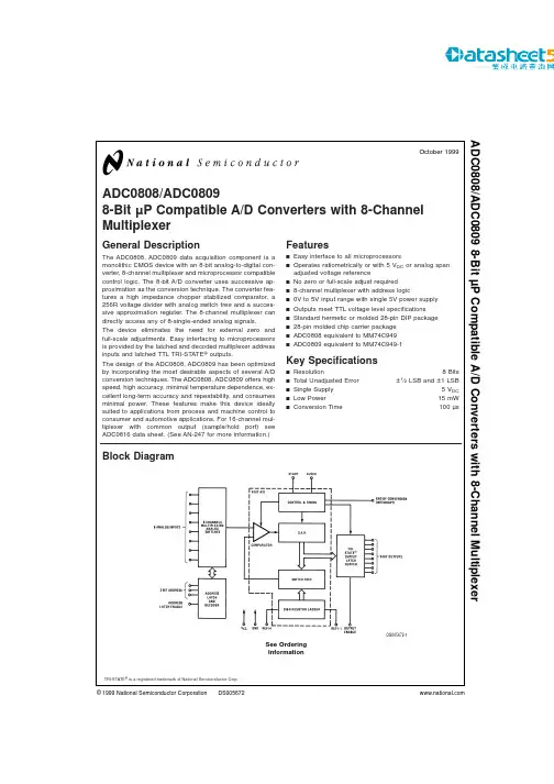
ADC0808/ADC08098-BitµP Compatible A/D Converters with8-ChannelMultiplexerGeneral DescriptionThe ADC0808,ADC0809data acquisition component is a monolithic CMOS device with an8-bit analog-to-digital con-verter,8-channel multiplexer and microprocessor compatible control logic.The8-bit A/D converter uses successive ap-proximation as the conversion technique.The converter fea-tures a high impedance chopper stabilized comparator,a 256R voltage divider with analog switch tree and a succes-sive approximation register.The8-channel multiplexer can directly access any of8-single-ended analog signals.The device eliminates the need for external zero and full-scale adjustments.Easy interfacing to microprocessors is provided by the latched and decoded multiplexer address inputs and latched TTL TRI-STATE®outputs.The design of the ADC0808,ADC0809has been optimized by incorporating the most desirable aspects of several A/D conversion techniques.The ADC0808,ADC0809offers high speed,high accuracy,minimal temperature dependence,ex-cellent long-term accuracy and repeatability,and consumes minimal power.These features make this device ideally suited to applications from process and machine control to consumer and automotive applications.For16-channel mul-tiplexer with common output(sample/hold port)see ADC0816data sheet.(See AN-247for more information.)Featuresn Easy interface to all microprocessorsn Operates ratiometrically or with5V DC or analog span adjusted voltage referencen No zero or full-scale adjust requiredn8-channel multiplexer with address logicn0V to5V input range with single5V power supplyn Outputs meet TTL voltage level specificationsn Standard hermetic or molded28-pin DIP packagen28-pin molded chip carrier packagen ADC0808equivalent to MM74C949n ADC0809equivalent to MM74C949-1Key Specificationsn Resolution8Bits n Total Unadjusted Error±1⁄2LSB and±1LSB n Single Supply5V DC n Low Power15mW n Conversion Time100µsBlock DiagramTRI-STATE®is a registered trademark of National Semiconductor Corp.DS005672-1See OrderingInformationOctober1999ADC0808/ADC08098-BitµPCompatibleA/DConverterswith8-ChannelMultiplexer©1999National Semiconductor Corporation Connection DiagramsOrdering InformationTEMPERATURE RANGE −40˚C to +85˚C−55˚C to +125˚C Error±1⁄2LSB Unadjusted ADC0808CCN ADC0808CCV ADC0808CCJADC0808CJ±1LSB UnadjustedADC0809CCN ADC0809CCVPackage OutlineN28A Molded DIPV28A Molded Chip CarrierJ28A Ceramic DIPJ28A Ceramic DIPDual-In-Line PackageDS005672-11Order Number ADC0808CCN or ADC0809CCNSee NS Package J28A or N28AMolded Chip Carrier PackageDS005672-12Order Number ADC0808CCV or ADC0809CCVSee NS Package V28AA D C 0808/A D C 0809 2Absolute Maximum Ratings(Notes2,1)If Military/Aerospace specified devices are required, please contact the National Semiconductor Sales Office/ Distributors for availability and specifications.Supply Voltage(V CC)(Note3) 6.5V Voltage at Any Pin−0.3V to(V CC+0.3V) Except Control InputsVoltage at Control Inputs−0.3V to+15V (START,OE,CLOCK,ALE,ADD A,ADD B,ADD C) Storage Temperature Range−65˚C to+150˚C Package Dissipation at T A=25˚C875mW Lead Temp.(Soldering,10seconds)Dual-In-Line Package(plastic)260˚CDual-In-Line Package(ceramic)300˚C Molded Chip Carrier PackageVapor Phase(60seconds)215˚C Infrared(15seconds)220˚C ESD Susceptibility(Note8)400VOperating Conditions(Notes1,2) Temperature Range(Note1)T MIN≤T A≤T MAX ADC0808CCN,ADC0809CCN−40˚C≤T A≤+85˚C ADC0808CCV,ADC0809CCV−40˚C≤T A≤+85˚C Range of V CC(Note1) 4.5V DC to6.0V DCElectrical CharacteristicsConverter Specifications:V CC=5V DC=V REF+,V REF(−)=GND,T MIN≤T A≤T MAX and f CLK=640kHz unless otherwise stated.Symbol Parameter Conditions Min Typ Max Units ADC0808Total Unadjusted Error25˚C±1⁄2LSB(Note5)T MIN to T MAX±3⁄4LSBADC0809Total Unadjusted Error0˚C to70˚C±1LSB(Note5)T MIN to T MAX±11⁄4LSBInput Resistance From Ref(+)to Ref(−) 1.0 2.5kΩAnalog Input Voltage Range(Note4)V(+)or V(−)GND−0.10V CC+0.10V DCV REF(+)Voltage,Top of Ladder Measured at Ref(+)V CC V CC+0.1VVoltage,Center of Ladder V CC/2-0.1V CC/2V CC/2+0.1VV REF(−)Voltage,Bottom of Ladder Measured at Ref(−)−0.10VI IN Comparator Input Current f c=640kHz,(Note6)−2±0.52µA Electrical CharacteristicsDigital Levels and DC Specifications:ADC0808CCN,ADC0808CCV,ADC0809CCN and ADC0809CCV,4.75≤V CC≤5.25V,−40˚C≤T A≤+85˚C unless otherwise notedSymbol Parameter Conditions Min Typ Max Units ANALOG MULTIPLEXERI OFF(+)OFF Channel Leakage Current V CC=5V,V IN=5V,T A=25˚C10200nAT MIN to T MAX 1.0µAI OFF(−)OFF Channel Leakage Current V CC=5V,V IN=0,T A=25˚C−200−10nAT MIN to T MAX−1.0µA CONTROL INPUTSV IN(1)Logical“1”Input Voltage V CC−1.5VV IN(0)Logical“0”Input Voltage 1.5VI IN(1)Logical“1”Input Current V IN=15V 1.0µA(The Control Inputs)I IN(0)Logical“0”Input Current V IN=0−1.0µA(The Control Inputs)I CC Supply Current f CLK=640kHz0.3 3.0mAADC0808/ADC08093Electrical Characteristics(Continued)Digital Levels and DC Specifications:ADC0808CCN,ADC0808CCV,ADC0809CCN and ADC0809CCV,4.75≤V CC ≤5.25V,−40˚C ≤T A ≤+85˚C unless otherwise notedSymbol ParameterConditions MinTypMaxUnitsDATA OUTPUTS AND EOC (INTERRUPT)V OUT(1)Logical “1”Output VoltageV CC =4.75V I OUT =−360µA I OUT =−10µA 2.44.5V(min)V(min)V OUT(0)Logical “0”Output Voltage I O =1.6mA 0.45V V OUT(0)Logical “0”Output Voltage EOC I O =1.2mA 0.45V I OUTTRI-STATE Output CurrentV O =5V 3µA V O =0−3µAElectrical CharacteristicsTiming Specifications V CC =V REF(+)=5V,V REF(−)=GND,t r =t f =20ns and T A =25˚C unless otherwise noted.Symbol ParameterConditionsMIn Typ Max Units t WS Minimum Start Pulse Width (Figure 5)100200ns t WALE Minimum ALE Pulse Width (Figure 5)100200ns t s Minimum Address Set-Up Time (Figure 5)2550ns t H Minimum Address Hold Time (Figure 5)2550ns t D Analog MUX Delay Time R S =0Ω(Figure 5)1 2.5µs From ALEt H1,t H0OE Control to Q Logic State C L =50pF,R L =10k (Figure 8)125250ns t 1H ,t 0H OE Control to Hi-Z C L =10pF,R L =10k (Figure 8)125250ns t c Conversion Time f c =640kHz,(Figure 5)(Note 7)90100116µs f c Clock Frequency 106401280kHz t EOC EOC Delay Time (Figure 5)08+2µSClock Periods C IN Input Capacitance At Control Inputs 1015pF C OUTTRI-STATE Output At TRI-STATE Outputs1015pFCapacitanceNote 1:Absolute Maximum Ratings indicate limits beyond which damage to the device may occur.DC and AC electrical specifications do not apply when operating the device beyond its specified operating conditions.Note 2:All voltages are measured with respect to GND,unless othewise specified.Note 3:A zener diode exists,internally,from V CC to GND and has a typical breakdown voltage of 7V DC .Note 4:Two on-chip diodes are tied to each analog input which will forward conduct for analog input voltages one diode drop below ground or one diode drop greater than the V CC n supply.The spec allows 100mV forward bias of either diode.This means that as long as the analog V IN does not exceed the supply voltage by more than 100mV,the output code will be correct.To achieve an absolute 0V DC to 5V DC input voltage range will therefore require a minimum supply voltage of 4.900V DC over temperature variations,initial tolerance and loading.Note 5:Total unadjusted error includes offset,full-scale,linearity,and multiplexer errors.See Figure 3.None of these A/Ds requires a zero or full-scale adjust.How-ever,if an all zero code is desired for an analog input other than 0.0V,or if a narrow full-scale span exists (for example:0.5V to 4.5V full-scale)the reference voltages can be adjusted to achieve this.See Figure 13.Note 6:Comparator input current is a bias current into or out of the chopper stabilized comparator.The bias current varies directly with clock frequency and has little temperature dependence (Figure 6).See paragraph 4.0.Note 7:The outputs of the data register are updated one clock cycle before the rising edge of EOC.Note 8:Human body model,100pF discharged through a 1.5k Ωresistor.A D C 0808/A D C 0809 4Functional DescriptionMultiplexer.The device contains an 8-channel single-ended analog signal multiplexer.A particular input channel is se-lected by using the address decoder.Table 1shows the input states for the address lines to select any channel.The ad-dress is latched into the decoder on the low-to-high transition of the address latch enable signal.TABLE 1.SELECTED ADDRESS LINE ANALOG CHANNELC B A IN0L L L IN1L L H IN2L H L IN3L H H IN4H L L IN5H L H IN6H H L IN7HHHCONVERTER CHARACTERISTICS The ConverterThe heart of this single chip data acquisition system is its 8-bit analog-to-digital converter.The converter is designed to give fast,accurate,and repeatable conversions over a wide range of temperatures.The converter is partitioned into 3major sections:the 256R ladder network,the successive ap-proximation register,and the comparator.The converter’s digital outputs are positive true.The 256R ladder network approach (Figure 1)was chosen over the conventional R/2R ladder because of its inherent monotonicity,which guarantees no missing digital codes.Monotonicity is particularly important in closed loop feedback control systems.A non-monotonic relationship can cause os-cillations that will be catastrophic for the system.Additionally,the 256R network does not cause load variations on the ref-erence voltage.The bottom resistor and the top resistor of the ladder net-work in Figure 1are not the same value as the remainder of the network.The difference in these resistors causes the output characteristic to be symmetrical with the zero and full-scale points of the transfer curve.The first output transi-tion occurs when the analog signal has reached +1⁄2LSB and succeeding output transitions occur every 1LSB later up to full-scale.The successive approximation register (SAR)performs 8it-erations to approximate the input voltage.For any SAR type converter,n-iterations are required for an n-bit converter.Figure 2shows a typical example of a 3-bit converter.In the ADC0808,ADC0809,the approximation technique is ex-tended to 8bits using the 256R network.The A/D converter’s successive approximation register (SAR)is reset on the positive edge of the start conversion (SC)pulse.The conversion is begun on the falling edge of the start conversion pulse.A conversion in process will be in-terrupted by receipt of a new start conversion pulse.Con-tinuous conversion may be accomplished by tying the end-of-conversion (EOC)output to the SC input.If used in this mode,an external start conversion pulse should be ap-plied after power up.End-of-conversion will go low between 0and 8clock pulses after the rising edge of start conversion.The most important section of the A/D converter is the com-parator.It is this section which is responsible for the ultimate accuracy of the entire converter.It is also the comparator drift which has the greatest influence on the repeatability of the device.A chopper-stabilized comparator provides the most effective method of satisfying all the converter require-ments.The chopper-stabilized comparator converts the DC input signal into an AC signal.This signal is then fed through a high gain AC amplifier and has the DC level restored.This technique limits the drift component of the amplifier since the drift is a DC component which is not passed by the AC am-plifier.This makes the entire A/D converter extremely insen-sitive to temperature,long term drift and input offset errors.Figure 4shows a typical error curve for the ADC0808as measured using the procedures outlined in AN-179.ADC0808/ADC08095Functional Description(Continued)DS005672-2FIGURE 1.Resistor Ladder and Switch TreeDS005672-13FIGURE 2.3-Bit A/D Transfer CurveDS005672-14FIGURE 3.3-Bit A/D Absolute Accuracy CurveDS005672-15FIGURE 4.Typical Error CurveA D C 0808/A D C 0809 6ADC0808/ADC0809Timing Diagram ArrayDS005672-4FIGURE5.7Typical PerformanceCharacteristicsTRI-STATE Test Circuits and Timing DiagramsApplications InformationOPERATION1.0RATIOMETRIC CONVERSIONThe ADC0808,ADC0809is designed as a complete Data Acquisition System (DAS)for ratiometric conversion sys-tems.In ratiometric systems,the physical variable being measured is expressed as a percentage of full-scale which is not necessarily related to an absolute standard.The voltage input to the ADC0808is expressed by the equation(1)V IN =Input voltage into the ADC0808V fs =Full-scale voltage V Z =Zero voltageD X =Data point being measured D MAX =Maximum data limit D MIN =Minimum data limitA good example of a ratiometric transducer is a potentiom-eter used as a position sensor.The position of the wiper is di-rectly proportional to the output voltage which is a ratio of the full-scale voltage across it.Since the data is represented as a proportion of full-scale,reference requirements are greatly reduced,eliminating a large source of error and cost for many applications.A major advantage of the ADC0808,ADC0809is that the input voltage range is equal to the sup-ply range so the transducers can be connected directly across the supply and their outputs connected directly into the multiplexer inputs,(Figure 9).Ratiometric transducers such as potentiometers,strain gauges,thermistor bridges,pressure transducers,etc.,are suitable for measuring proportional relationships;however,many types of measurements must be referred to an abso-lute standard such as voltage or current.This means a sys-DS005672-16FIGURE parator I IN vs V IN(V CC =V REF =5V)DS005672-17FIGURE 7.Multiplexer R ON vs V IN(V CC =V REF =5V)t 1H ,t H1DS005672-18t 1H ,C L =10pFDS005672-19t H1,C L =50pFDS005672-20t 0H ,t H0DS005672-21t 0H ,C L =10pF DS005672-22t H0,C L =50pFDS005672-23FIGURE 8.A D C 0808/A D C 08098Applications Information(Continued)tem reference must be used which relates the full-scale volt-age to the standard volt.For example,if V CC=V REF=5.12V, then the full-scale range is divided into256standard steps. The smallest standard step is1LSB which is then20mV.2.0RESISTOR LADDER LIMITATIONSThe voltages from the resistor ladder are compared to the selected into8times in a conversion.These voltages are coupled to the comparator via an analog switch tree which is referenced to the supply.The voltages at the top,center and bottom of the ladder must be controlled to maintain proper operation.The top of the ladder,Ref(+),should not be more positive than the supply,and the bottom of the ladder,Ref(−),should not be more negative than ground.The center of the ladder voltage must also be near the center of the supply because the analog switch tree changes from N-channel switches to P-channel switches.These limitations are automatically sat-isfied in ratiometric systems and can be easily met in ground referenced systems.Figure10shows a ground referenced system with a sepa-rate supply and reference.In this system,the supply must be trimmed to match the reference voltage.For instance,if a 5.12V is used,the supply should be adjusted to the same voltage within0.1V.The ADC0808needs less than a milliamp of supply current so developing the supply from the reference is readily ac-complished.In Figure11a ground referenced system is shown which generates the supply from the reference.The buffer shown can be an op amp of sufficient drive to supply the milliamp of supply current and the desired bus drive,or if a capacitive bus is driven by the outputs a large capacitor will supply the transient supply current as seen in Figure12.The LM301is overcompensated to insure stability when loaded by the10µF output capacitor.The top and bottom ladder voltages cannot exceed V CC and ground,respectively,but they can be symmetrically less than V CC and greater than ground.The center of the ladder volt-age should always be near the center of the supply.The sen-sitivity of the converter can be increased,(i.e.,size of the LSB steps decreased)by using a symmetrical reference sys-tem.In Figure13,a2.5V reference is symmetrically cen-tered about V CC/2since the same current flows in identical resistors.This system with a2.5V reference allows the LSB bit to be half the size of a5V reference system.DS005672-7FIGURE9.Ratiometric Conversion SystemADC0808/ADC08099Applications Information(Continued)DS005672-24FIGURE 10.Ground ReferencedConversion System Using Trimmed SupplyDS005672-25FIGURE 11.Ground Referenced Conversion System withReference Generating V CC SupplyA D C 0808/A D C 0809 10Applications Information(Continued)3.0CONVERTER EQUATIONSThe transition between adjacent codes N and N+1is givenby:(2)The center of an output code N is given by:(3)The output code N for an arbitrary input are the integerswithin the range:(4)Where:V IN=Voltage at comparator inputV REF(+)=Voltage at Ref(+)V REF(−)=Voltage at Ref(−)V TUE=Total unadjusted error voltage(typicallyV REF(+)÷512)DS005672-26FIGURE12.Typical Reference and Supply CircuitDS005672-27R A=R B*Ratiometric transducersFIGURE13.Symmetrically Centered ReferenceADC0808/ADC080911Applications Information(Continued)4.0ANALOG COMPARATOR INPUTS The dynamic comparator input current is caused by the pe-riodic switching of on-chip stray capacitances.These are connected alternately to the output of the resistor ladder/switch tree network and to the comparator input as part of the operation of the chopper stabilized comparator.The average value of the comparator input current varies di-rectly with clock frequency and with V IN as shown in Figure 6.If no filter capacitors are used at the analog inputs and the signal source impedances are low,the comparator input cur-rent should not introduce converter errors,as the transient created by the capacitance discharge will die out before the comparator output is strobed.If input filter capacitors are desired for noise reduction and signal conditioning they will tend to average out the dynamic comparator input current.It will then take on the characteris-tics of a DC bias current whose effect can be predicted con-ventionally.Typical ApplicationTABLE 2.Microprocessor Interface TablePROCESSORREAD WRITE INTERRUPT (COMMENT)8080MEMR MEMW INTR (Thru RST Circuit)8085RD WR INTR (Thru RST Circuit)Z-80RD WR INT (Thru RST Circuit,Mode 0)SC/MPNRDS NWDS SA (Thru Sense A)6800VMA •φ2•R/W VMA •φ•R/W IRQA or IRQB (Thru PIA)DS005672-10*Address latches needed for 8085and SC/MP interfacing the ADC0808to a microprocessorA D C 0808/A D C 12Physical Dimensions inches(millimeters)unless otherwise notedMolded Dual-In-Line Package (N)Order Number ADC0808CCN or ADC0809CCNNS Package Number N28BMolded Chip Carrier (V)Order Number ADC0808CCV or ADC0809CCVNS Package Number V28AADC0808/13Notes LIFE SUPPORT POLICY NATIONAL’S PRODUCTS ARE NOT AUTHORIZED FOR USE AS CRITICAL COMPONENTS IN LIFE SUPPORT DEVICES OR SYSTEMS WITHOUT THE EXPRESS WRITTEN APPROVAL OF THE PRESIDENT AND GENERAL COUNSEL OF NATIONAL SEMICONDUCTORCORPORATION.As used herein:1.Life support devices or systems are devices or systems which,(a)are intended for surgical implantinto the body,or (b)support or sustain life,and whose failure to perform when properly used in accordance with instructions for use provided in the labeling,can be reasonably expected to result in a significant injury to the user.2.A critical component is any component of a life support device or system whose failure to perform can be reasonably expected to cause the failure of the life support device or system,or to affect its safety or effectiveness.National SemiconductorCorporationAmericasTel:1-800-272-9959Fax:1-800-737-7018Email:support@National Semiconductor Europe Fax:+49(0)180-5308586Email:europe.support@ Deutsch Tel:+49(0)180-5308585English Tel:+49(0)180-5327832Français Tel:+49(0)180-5329358Italiano Tel:+49(0)180-5341680National Semiconductor Asia Pacific Customer Response Group Tel:65-2544466Fax:65-2504466Email:sea.support@ National Semiconductor Japan Ltd.Tel:81-3-5639-7560Fax:81-3-5639-7507 A D C 0808/A D C 08098-B i t µP C o m p a t i b l e A /D C o n v e r t e r s w i t h 8-C h a n n e l M u l t i p l e x e r National does not assume any responsibility for use of any circuitry described,no circuit patent licenses are implied and National reserves the right at any time without notice to change said circuitry and specifications.。
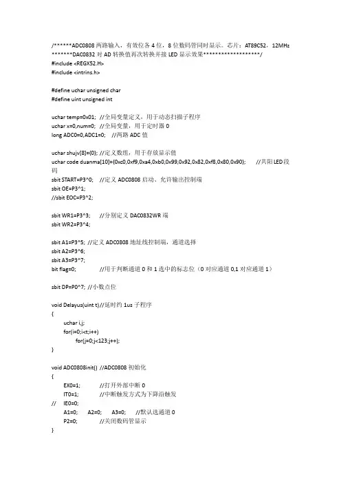
/******ADC0808两路输入,有效位各4位,8位数码管同时显示。
芯片:AT89C52,12MHz *******DAC0832对AD转换值再次转换并接LED显示效果*******************/#include <REGX52.H>#include <intrins.h>#define uchar unsigned char#define uint unsigned intuchar temp=0x01; //全局变量定义,用于动态扫描子程序uchar x=0,num=0; //全局变量,用于定时器0long ADC0=0,ADC1=0; //两路ADC值uchar shujv[8]={0}; //定义数组,用于存放显示值uchar code duanma[10]={0xc0,0xf9,0xa4,0xb0,0x99,0x92,0x82,0xf8,0x80,0x90}; //共阳LED段码sbit START=P3^0; //定义ADC0808启动、允许输出控制端sbit OE=P3^1;//sbit EOC=P3^2;sbit WR1=P3^3; //分别定义DAC0832WR端sbit WR2=P3^4;sbit A1=P3^5; //定义ADC0808地址线控制端,通道选择sbit A2=P3^6;sbit A3=P3^7;bit flag=0; //用于判断通道0和1选中的标志位(0对应通道0,1对应通道1)sbit DP=P0^7; //小数点位void Delayus(uint t) //延时约1us子程序{uchar i,j;for(i=0;i<t;i++)for(j=0;j<123;j++);}void ADC0808init() //ADC0808初始化{EX0=1; //打开外部中断0IT0=1; //中断触发方式为下降沿触发// IE0=0;A1=0; A2=0; A3=0; //默认选通道0P2=0; //关闭数码管显示}void timer0init() //定时器0初始化,用于LED动态扫描{TMOD=0X02; //定时器0工作于方式2TH0=0X38; //赋初值,12MHz,定时200微秒TL0=0X38;EA=1; //开总中断ET0=1; //开定时器0中断TR0=1; //启动定时器0}void display() //数码管显示函数{P2=0; //消隐P0=duanma[shujv[x]]; //将处理后段码值传给数码管if(x==0 || x==4) //若扫描到第0位和第4位则显示小数点位,由于段码表中均为不含小数点位的段码,顾不需写else=1语句DP=0;P2=temp; //打开位选使相应的数码管显示,其余数码管关闭if(++x>=8) //扫描一遍后重新归零x=0;temp=_crol_(temp,1); //循环左移}void ADCconver() //ADC0808转换子程序{OE=0; //禁止输出START=0; //START置低A1=~A1; //ALE为0,此时改变地址进行通道0和1切换if(A1==1) //判断是否为通道1flag=1;START=1; _nop_(); //START拉高产生上升沿从而使内部所有寄存器清零START=0; //再拉低产生下降沿,开始AD转换,转换完成后EOC会产生上升沿,加反相器后变成下降沿进而触发外部中断}void shujvchuli() //数据处理子函数{long temp1=((ADC0*1000)/51),temp2=((ADC1*1000)/51); //N*5/256,乘1000是为了变为4位整数,便于后续各位分离shujv[0]=temp1/1000; //通道0千位shujv[1]=temp1/100%10; //通道0百位shujv[2]=temp1%100/10; //通道0十位shujv[3]=temp1%10; //通道0个位shujv[4]=temp2/1000; //通道1千位shujv[5]=temp2/100%10; //通道1百位shujv[6]=temp2%100/10; //通道1十位shujv[7]=temp2%10; //通道1个位}void main(){timer0init(); //定时器0初始化ADC0808init(); //ADC0808初始化while(1){ADCconver(); //ADC开始转换shujvchuli(); //进行数据处理装换}}void timer0() interrupt 1 //定时器0中断服务程序,数码管定时扫描{if(++num>=10) //0.2*10=2ms,2ms进行一次显示{num=0; //清零,重新开始累加计时display(); //显示}}void inter() interrupt 0 //外部中断0中断服务程序(中断法检测EOC){/* EX0=0; //考虑到中断虽不由程序控制,但外部期间由程序控制,这样中断间接受程序控制,下次中断的触发在中断服务程序执行后才会发生*/OE=1; //收到转换结束信号则允许输出if(flag) //如果是通道1选通,将装换完成的值赋给变量ADD1,否则赋值给ADD0 {flag=0; //通道标志清零ADC1=P1;WR2=0; //写信号允许,打开第二个DAC0832输入缓存器WR2=1; //数据送入后关闭输入,防止数据变化Delayus(1); //延时使DA转换完成,防止未转换完成情况下再次送入数据}else{ADC0=P1;WR1=0; //写信号允许,打开第一个DAC0832输入缓存器WR1=1; //数据送入后关闭输入,防止数据变化Delayus(1); //延时使DA转换完成,防止未转换完成情况下再次送入数据}OE=0; //未收到转换完成信号则禁止ADC0808输出数据// EX0=1;}。

ADC0808是一款八位A/D转换器,可以将模拟信号转换成数字信号来计算机处理。
它可以将输入的模拟电压信号转换为相应的数字值,实现电压信号的转化。
ADC0808的工作原理是基于逐次逼近法的。
在逐次逼近法中,首先将输入电压与参考电压进行比较,然后根据比较结果来调整数字值,直到得到最终的数字值。
ADC0808内部包含一个多位比较器、一个数据暂存器、一个内部时钟、一个参考电压源和一个缓冲放大器等部件。
当ADC0808接收到模拟电压信号时,首先通过缓冲放大器将信号进行放大和缓冲,然后通过定时器进行时间分解,将模拟信号转换成位值。
接下来,通过放大器将位值变成比较电压,多位比较器比较这些比较电压与模拟信号之间的差值,并把结果存储在数据暂存器中。
最终,通过逐次逼近法得到转换后的数字值。
需要注意的是,ADC0808的转换精度和速度会受到多种因素的影响,如输入信号的幅度、频率、噪声等。
因此,在使用ADC0808进行电压信号转化时,需要根据实际情况进行选择和调整。

11.2.4 典型的集成ADC芯片为了满足多种需要,目前国内外各半导体器件生产厂家设计并生产出了多种多样的ADC芯片。
仅美国AD公司的ADC产品就有几十个系列、近百种型号之多。
从性能上讲,它们有的精度高、速度快,有的则价格低廉。
从功能上讲,有的不仅具有A/D转换的基本功能,还包括内部放大器和三态输出锁存器;有的甚至还包括多路开关、采样保持器等,已发展为一个单片的小型数据采集系统。
尽管ADC芯片的品种、型号很多,其内部功能强弱、转换速度快慢、转换精度高低有很大差别,但从用户最关心的外特性看,无论哪种芯片,都必不可少地要包括以下四种基本信号引脚端:模拟信号输入端(单极性或双极性);数字量输出端(并行或串行);转换启动信号输入端;转换结束信号输出端.除此之外,各种不同型号的芯片可能还会有一些其他各不相同的控制信号端。
选用ADC芯片时,除了必须考虑各种技术要求外,通常还需了解芯片以下两方面的特性。
(1)数字输出的方式是否有可控三态输出。
有可控三态输出的ADC芯片允许输出线与微机系统的数据总线直接相连,并在转换结束后利用读数信号RD选通三态门,将转换结果送上总线。
没有可控三态输出(包括内部根本没有输出三态门和虽有三态门、但外部不可控两种情况)的ADC芯片则不允许数据输出线与系统的数据总线直接相连,而必须通过I/O接口与MPU交换信息。
(2)启动转换的控制方式是脉冲控制式还是电平控制式。
对脉冲启动转换的ADC 芯片,只要在其启动转换引脚上施加一个宽度符合芯片要求的脉冲信号,就能启动转换并自动完成。
一般能和MPU配套使用的芯片,MPU的I/O写脉冲都能满足ADC芯片对启动脉冲的要求.对电平启动转换的ADC芯片,在转换过程中启动信号必须保持规定的电平不变,否则,如中途撤消规定的电平,就会停止转换而可能得到错误的结果。
为此,必须用D触发器或可编程并行I/O接口芯片的某一位来锁存这个电平,或用单稳等电路来对启动信号进行定时变换.具有上述两种数字输出方式和两种启动转换控制方式的ADC芯片都不少,在实际使用芯片时要特别注意看清芯片说明。