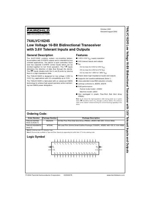
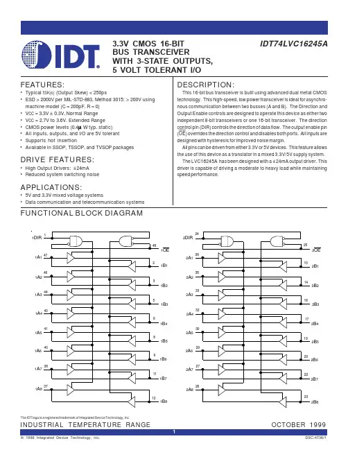
MC74LCX16245Low−Voltage CMOS16−Bit TransceiverWith 5 V−Tolerant Inputs and Outputs(3−State, Non−Inverting)The MC74LCX16245 is a high performance, non−inverting 16−bittransceiver operating from a 2.3 to 3.6 V supply. The device is byte controlled. Each byte has separate Output Enable inputs which can be tied together for full 16−bit operation. High impedance TTL compatible inputs significantly reduce current loading to input drivers while TTL compatible outputs offer improved switching noise performance. A V I specification of 5.5 V allows MC74LCX16245 inputs to be safely driven from 5.0 V devices. The MC74LCX16245 is suitable for memory address driving and all TTL level bus oriented transceiver applications.The 4.5 ns maximum propagation delays support high performance applications. Current drive capability is 24 mA at both A and B ports. The Transmit/Receive (T/Rn) inputs determine the direction of data flow through the bidirectional transceiver. Transmit (active−HIGH) enables data from A ports to B ports; Receive (active−LOW) enables data from B to A ports. The Output Enable inputs (OEn), when HIGH, disable both A and B ports by placing them in a HIGH Z condition. Features•Designed for 2.3 to 3.6 V V CC Operation•4.5 ns Maximum t pd•5.0 V Tolerant − Interface Capability With 5.0 V TTL Logic •Supports Live Insertion and Withdrawal•I OFF Specification Guarantees High Impedance When V CC = 0 V •LVTTL Compatible•LVCMOS Compatible•24 mA Balanced Output Sink and Source Capability•Near Zero Static Supply Current in All Three Logic States (20 m A) Substantially Reduces System Power Requirements •Latchup Performance Exceeds 500 mA•ESD Performance:Human Body Model >2000 V;Machine Model >200 V•These are Pb−Free Devices**For additional information on our Pb−Free strategy and soldering details, please download the ON Semiconductor Soldering and Mounting Techniques Reference Manual, SOLDERRM/D.See detailed ordering and shipping information in the package dimensions section on page 3 of this data sheet.ORDERING INFORMATIONFigure 1. Pinout: 48−Lead (Top View)481OE1T/R1472A0B0463A1B1454GND GND 445A2B2436A3B3427V CC V CC 418A4B4409A5B53910GND GND 3811A6B63712A7B73613A8B83514A9B93415GND GND 3316A10B103217A11B113118V CC V CC 3019A12B122920A13B132821GND GND 2722A14B142623A15B152524OE2T/R2Table 1. PIN NAMESPinsFunctionOEn T/Rn A0 − A15B0 − B15Output Enable Inputs Transmit/Receive InputsSide A Inputs or 3−State Outputs Side B Inputs or 3−State OutputsT/R1Figure 2. Logic DiagramTRUTH TABLEInputs OutputsInputsOutputsOE1T/R1OE2T/R2L L Bus B0:7 Data to Bus A0:7L L Bus B8:15 Data to Bus A8:15L H Bus A0:7 Data to Bus B0:7L H Bus A8:15 Data to Bus B8:15H XHigh Z State on A0:7, B0:7HXHigh Z State on A8:15, B8:15H =High Voltage Level L =Low Voltage Level Z =High Impedance StateX=High or Low Voltage Level and Transitions Are Acceptable; for I CC reasons, DO NOT FLOAT InputsORDERING INFORMATIONDevice Package Shipping†MC74LCX16245DT TSSOP−48*39 Units / RailMC74LCX16245DTG TSSOP−48*39 Units / RailMC74LCX16245DTR2TSSOP−48*2500 / Tape & ReelM74LCX16245DTR2G TSSOP−48*2500 / Tape & Reel†For information on tape and reel specifications, including part orientation and tape sizes, please refer to our Tape and Reel Packaging Specifications Brochure, BRD8011/D.*This package is inherently Pb−Free.MAXIMUM RATINGSSymbol Parameter Value Condition Unit V CC DC Supply Voltage−0.5 to +7.0V V I DC Input Voltage−0.5 ≤ V I≤ +7.0V V O DC Output Voltage−0.5 ≤ V O≤ +7.0Output in 3−State V−0.5 ≤ V O≤ V CC + 0.5Output in HIGH or LOW State. (Note 1)VI IK DC Input Diode Current−50V I < GND mAI OK DC Output Diode Current−50V O < GND mA+50V O > V CC mAI O DC Output Source/Sink Current±50mAI CC DC Supply Current Per Supply Pin±100mAI GND DC Ground Current Per Ground Pin±100mAT STG Storage Temperature Range−65 to +150°C Maximum ratings are those values beyond which device damage can occur. Maximum ratings applied to the device are individual stress limit values (not normal operating conditions) and are not valid simultaneously. If these limits are exceeded, device functional operation is not implied, damage may occur and reliability may be affected.1.I O absolute maximum rating must be observed.RECOMMENDED OPERATING CONDITIONSSymbol Parameter Min Typ Max UnitV CC Supply Voltage OperatingData Retention Only 2.01.52.5,3.32.5,3.33.63.6VV I Input Voltage0 5.5VV O Output Voltage(HIGH or LOW State)(3−State)0V CC5.5VI OH HIGH Level Output Current V CC = 3.0 V − 3.6 VV CC = 2.7 V − 3.0 VV CC = 2.3 V − 2.7 V − 24− 12− 8mAI OL LOW Level Output Current V CC = 3.0 V − 3.6 VV CC = 2.7 V − 3.0 VV CC = 2.3 V − 2.7 V + 24+ 12+ 8mAT A Operating Free−Air Temperature−40+85°C D t/D V Input Transition Rise or Fall Rate, V IN from 0.8 V to 2.0 V, V CC = 3.0 V010ns/VDC ELECTRICAL CHARACTERISTICSSymbol Characteristic Condition T A = −40°C to +85°CUnit Min MaxV IH HIGH Level Input Voltage (Note 2) 2.3 V ≤ V CC≤ 2.7 V 1.7V2.7 V ≤ V CC≤3.6 V 2.0V IL LOW Level Input Voltage (Note 2) 2.3 V ≤ V CC≤ 2.7 V0.7V2.7 V ≤ V CC≤3.6 V0.8V OH HIGH Level Output Voltage 2.3 V ≤ V CC≤ 3.6 V; I OL = 100 m A V CC−0.2VV CC = 2.3 V; I OH = −8 mA 1.8V CC = 2.7 V; I OH = −12 mA 2.2V CC = 3.0 V; I OH = −18 mA 2.4V CC = 3.0 V; I OH = −24 mA 2.2 V OL LOW Level Output Voltage 2.3 V ≤ V CC≤ 3.6 V; I OL = 100 m A0.2VV CC = 2.3 V; I OL= 8 mA0.6V CC = 2.7 V; I OL= 12 mA0.4V CC = 3.0 V; I OL = 16 mA0.4V CC = 3.0 V; I OL = 24 mA0.55I I Input Leakage Current 2.3 V ≤ V CC≤ 3.6 V; 0 V ≤ V I≤ 5.5 V±5.0m AI OZ3−State Output Current 2.3 ≤ V CC≤ 3.6 V; 0V ≤ V O≤ 5.5 V;V I = V IH or V IL±5.0m AI OFF Power−Off Leakage Current V CC = 0 V; V I or V O = 5.5 V10m AI CC Quiescent Supply Current 2.3 ≤ V CC≤ 3.6 V; V I = GND or V CC20m A2.3 ≤ V CC≤3.6 V; 3.6 ≤ V I or V O≤ 5.5 V±20m AD I CC Increase in I CC per Input 2.3 ≤ V CC≤ 3.6 V; V IH = V CC − 0.6 V500m A2.These values of V I are used to test DC electrical characteristics only.AC CHARACTERISTICS t R = t F = 2.5 ns; R L = 500 WSymbol Parameter WaveformT A = −40°C to +85°CUnit V CC = 3.3 V ± 0.3 VC L = 50 pFV CC = 2.7 VC L = 50 pFV CC = 2.5 V ± 0.2 VC L = 30 pFMin Max Min Max Min Maxt PLH t PHL Propagation DelayInput to Output1 1.51.54.54.51.51.55.25.21.51.55.45.4nst PZH t PZL Output Enable Time toHigh and Low Level2 1.51.56.56.51.51.57.27.21.51.58.58.5nst PHZ t PLZ Output Disable Time FromHigh and Low Level2 1.51.56.46.41.51.56.96.91.51.57.77.7nst OSHL t OSLH Output−to−Output Skew(Note 3)1.01.0ns3.Skew is defined as the absolute value of the difference between the actual propagation delay for any two separate outputs of the same device.The specification applies to any outputs switching in the same direction, either HIGH−to−LOW (t OSHL) or LOW−to−HIGH (t OSLH); parameter guaranteed by design.DYNAMIC SWITCHING CHARACTERISTICSSymbol Characteristic ConditionT A = +25°CUnit Min Typ MaxV OLP Dynamic LOW Peak Voltage(Note 4)V CC = 3.3 V, C L = 50 pF, V IH = 3.3 V, V IL = 0 VV CC = 2.5 V, C L = 30 pF, V IH = 2.5 V, V IL = 0 V0.80.6VVV OLV Dynamic LOW Valley Voltage (Note 4)V CC = 3.3 V, C L = 50 pF, V IH = 3.3 V, V IL = 0 VV CC = 2.5 V, C L = 30 pF, V IH = 2.5 V, V IL = 0 V−0.8−0.6VV4.Number of outputs defined as “n”. Measured with “n−1” outputs switching from HIGH−to−LOW or LOW−to−HIGH. The remaining output ismeasured in the LOW state.CAPACITIVE CHARACTERISTICSSymbol Parameter Condition Typical UnitC IN Input Capacitance V CC = 3.3 V, V I = 0 V or V CC7pFC I/O Input/Output Capacitance V CC = 3.3 V, V I = 0 V or V CC8pFC PD Power Dissipation Capacitance10 MHz, V CC = 3.3 V, V I = 0 V or V CC20pFAn, Bn WAVEFORM 1 − PROPAGATION DELAYS t R = t F = 2.5 ns, 10% to 90%; f = 1 MHz; t W = 500 ns V CC0 VV OHV OLAn, BnBn, AnWAVEFORM 2 − OUTPUT ENABLE AND DISABLE TIMESt R = t F = 2.5 ns, 10% to 90%; f = 1 MHz; t W = 500 ns0 VOEn,T/RnAn, BnFigure 3. AC WaveformsV OH V HZ V OLV CCV LZ Table 2. AC WAVEFORMSSymbol V CC3.3 V ±0.3 V2.7 V 2.5 V +0.2 V Vmi 1.5 V 1.5 V V CC / 2Vmo 1.5 V 1.5 V V CC / 2V HZ V OL + 0.3 V V OL+ 0.3 V V OL + 0.15 V V LZV OH − 0.3 VV OH − 0.3 VV OH − 0.15 VOPEN V 6 V or V CC x 2GNDFigure 4. Test CircuitTable 3. TEST CIRCUITTESTSWITCH t PLH , t PHL Opent PZL , t PLZ6 V at V CC = 3.3 0.3 V 6 V at V CC = 2.5 0.2 VOpen Collector/Drain t PLH and t PHL 6 V t PZH , t PHZGNDC L = 50 pF at V CC = 3.3 0.3 V or equivalent (includes jig and probe capacitance)C L = 30 pF at V CC = 2.5 0.2 V or equivalent (includes jig and probe capacitance)R L = R 1 = 500 W or equivalentR T = Z OUT of pulse generator (typically 50 W )PACKAGE DIMENSIONSTSSOP−48DT SUFFIX CASE 1201−01ISSUE ADIM MIN MAX MIN MAX INCHESMILLIMETERS A 12.4012.600.4880.496B 6.00 6.200.2360.244C −−− 1.10−−−0.043D 0.050.150.0020.006F 0.500.750.0200.030G 0.50 BSC 0.0197 BSC H 0.37−−−0.015−−−J 0.090.200.0040.008J10.090.160.0040.006K 0.170.270.0070.011K10.170.230.0070.009L 7.958.250.3130.325M0 8 0 8 ____NOTES:1.DIMENSIONING AND TOLERANCING PER ANSI Y14.5M, 1982.2.CONTROLLING DIMENSION: MILLIMETER.3.DIMENSIONS A AND B DO NOT INCLUDE MOLD FLASH, PROTRUSIONS OR GATE BURRS. MOLD FLASH OR GATE BURRS SHALL NOT EXCEED 0.15 (0.006) PER SIDE.4.DIMENSION K DOES NOT INCLUDE DAMBAR PROTRUSION. ALLOWABLE DAMBARPROTRUSION SHALL BE 0.08 (0.003) TOTAL IN EXCESS OF THE K DIMENSION AT MAXIMUM MATERIAL CONDITION.5.TERMINAL NUMBERS ARE SHOWN FOR REFERENCE ONLY.6.DIMENSIONS A AND B ARE TO BE DETERMINED AT DATUM PLANE −W−.ON Semiconductor and are registered trademarks of Semiconductor Components Industries, LLC (SCILLC). SCILLC reserves the right to make changes without further notice to any products herein. SCILLC makes no warranty, representation or guarantee regarding the suitability of its products for any particular purpose, nor does SCILLC assume any liability arising out of the application or use of any product or circuit, and specifically disclaims any and all liability, including without limitation special, consequential or incidental damages.“Typical” parameters which may be provided in SCILLC data sheets and/or specifications can and do vary in different applications and actual performance may vary over time. All operating parameters, including “Typicals” must be validated for each customer application by customer’s technical experts. SCILLC does not convey any license under its patent rights nor the rights of others. SCILLC products are not designed, intended, or authorized for use as components in systems intended for surgical implant into the body, or other applications intended to support or sustain life, or for any other application in which the failure of the SCILLC product could create a situation where personal injury or death may occur. Should Buyer purchase or use SCILLC products for any such unintended or unauthorized application, Buyer shall indemnify and hold SCILLC and its officers, employees, subsidiaries, affiliates, and distributors harmless against all claims, costs, damages, and expenses, and reasonable attorney fees arising out of, directly or indirectly, any claim of personal injury or death associated with such unintended or unauthorized use, even if such claim alleges that SCILLC was negligent regarding the design or manufacture of the part. SCILLC is an Equal Opportunity/Affirmative Action Employer. This literature is subject to all applicable copyright laws and is not for resale in any manner.PUBLICATION ORDERING INFORMATION。