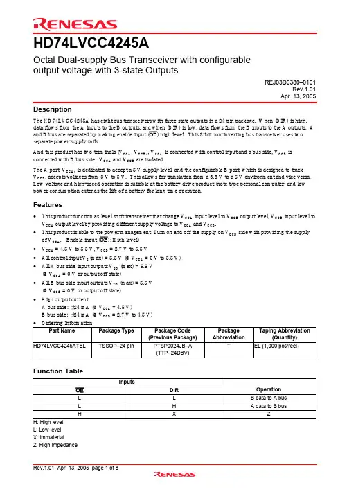
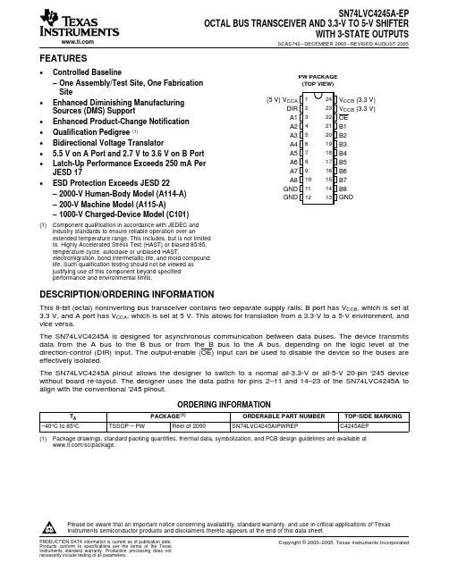
sn74lvc4245a具有三态输出的八路总线收发器和 3.3V 至 5V 移位器
- 格式:pdf
- 大小:398.90 KB
- 文档页数:15
1 引言近年来,随着便携式数字电子产品笔记本计算机、数字式移动电话、手持式测试仪表等的迅速发展,要求使用体积小、功耗低、电池耗电小的器件,数字系统的工作电压已经从5V降至3V甚至更低(例如2.5V 和1.8V标准的引进)。
但是目前仍有许多5V电源的逻辑器件和数字器件可用,因此在许多设计中3V(含3. 3V)逻辑系统和5V逻辑系统共存,而且不同的电源电压在同一电路板中混用。
随着更低电压标准的引进,不同电源电压逻辑器件问的接口问题会在很长一段时间内存在。
本文讨论的是使用TTL和CMOS的3V和5V系统中逻辑器件间接口的基本概念和电路实例。
理解了这些概念可避免不同电压的逻辑器件接口时出现的问题和保证所设计的电路数据传输的可靠性。
2 逻辑电平不同,接口时出现的问题在混合电压系统中,不同电源电压的逻辑器件相互接口时会存在以下3个主要问题:∙加到输入和输出引脚上允许的最大电压的限制问题;∙两个电源间电流的互串问题;∙必须满足的输入转换门限电平问题。
器件对加到输入脚或输出脚的电压通常是有限制的。
这些引脚有二极管或分离元件接到Vcc。
如果接入的电压过高,则电流将会通过二极管或分离元件流向电源。
例如3V器件的输入端接上5V信号,则5V电源将会向3V电源充电。
持续的电流将会损坏二极管和电路元件。
在等待或掉电方式时,3V电源降落到0V,大电流将流通到地,这使总线上的高电压被下拉到地,这些情况将引起数据丢失和元件损坏。
必须注意的是:不管是在3V的工作状态或是0V的等待状态部不允许电流流向Vcc。
另外用5V的器件来驱动3V的器件有很多不同情况,同样TTL和CMOS间的转换电平也存在不同情况。
驱动器必须满足接收器的输入转换电平,并要有足够的容限和保证不损坏电路元件。
以上问题在详细地分析一些具体电路后便会很清楚。
3 可用5V容限输入的3V逻辑器件3V的逻辑器件可以有5V输入容限的器件是LVC、LVT、ALVT、LCX、LVX、等系列。

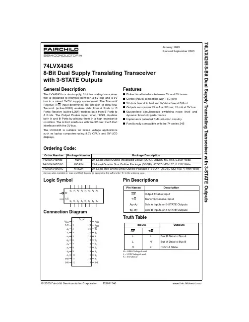
MC74LVX4245Dual Supply OctalTranslating Transceiverwith 3−State OutputsThe 74LVX4245 is a 24−pin dual−supply, octal translating transceiver that is designed to interface between a 5.0 V bus and a 3.0 V bus in a mixed 3.0 V / 5.0 V supply environment such as laptop computers using a 3.3 V CPU and 5.0 V LCD display. The A port interfaces with the 5V bus; the B port interfaces with the 3.0 V bus.The Transmit/Receive (T/R) input determines the direction of data flow. Transmit (active−High) enables data from the A port to the B port. Receive (active−Low) enables data from the B port to the A port.The Output Enable (OE) input, when High, disables both A and B ports by placing them in 3−State.Features•Bi−directional Interface Between 5.0 V and 3.0 V Buses •Control Inputs Compatible with TTL Level•5.0 V Data Flow at A Port and 3.0 V Data Flow at B Port•Outputs Source/Sink 24 mA at 5.0 V Bus and 12 mA at 3.0 V Bus •Guaranteed Simultaneous Switching Noise Level and Dynamic Threshold Performance•Available in SOIC and TSSOP Packages•Functionally Compatible with the 74 Series 245•Pb−Free Packages are Available*Figure 1. 24−Lead Pinout(Top View)232422212019182134567V CCB 1781691510V CCB OE B0B1B2B3B4B5B6V CCA T/RA0A1A2A3A4A5A6A714111312B7GND GND GND*For additional information on our Pb−Free strategy and soldering details, please download the ON Semiconductor Soldering and Mounting Techniques Reference Manual, SOLDERRM/D.MARKING DIAGRAMSSOIC−24See detailed ordering and shipping information in the package dimensions section on page 5 of this data sheet.ORDERING INFORMATION124LVXC4245AWLYYWW A =Assembly Location WL =Wafer Lot YY =YearWW =Work WeekLVX 4245AWLYYWW124TSSOP−24DT SUFFIX CASE 948HB0OE 22T/R 2A0B1A1B2A2B3A3B4A4B5A5B6A6B7A7Figure 2. Logic DiagramH = High Voltage Level; L = Low Voltage Level; Z = High Impedance State; X = High or Low Voltage Level and Transitions are Acceptable; For I CC reasons, Do Not Float InputsABSOLUTE MAXIMUM RATINGSvalues (not normal operating conditions) and are not valid simultaneously. If these limits are exceeded, device functional operation is not implied, damage may occur and reliability may be affected.RECOMMENDED OPERATING CONDITIONSDC ELECTRICAL CHARACTERISTICSDC ELECTRICAL CHARACTERISTICS2.Max number of outputs defined as (n). Data inputs are driven 0V to V CC level; one output at GND.3.Max number of data inputs (n) switching. (n−1) inputs switching 0V to V CC level. Input under test switching: V CC level to threshold (V IHD),0V to threshold (V ILD), f = 1MHz.CAPACITIVE CHARACTERISTICSAC ELECTRICAL CHARACTERISTICSCCA CCB5.Skew is defined as the absolute value of the difference between the actual propagation delay for any two separate outputs of the same device.The specification applies to any outputs switching in the same direction, either HIGH−to−LOW (t OSHL) or LOW−to−HIGH (t OSLH); parameter guaranteed by design.ORDERING INFORMATIONSpecifications Brochure, BRD8011/D.*This package is inherently Pb−Free.Dual Supply Octal Translating TransceiverThe 74LVX4245 is a is a dual−supply device well capable of bidirectional signal voltage translation. This level shifting ability provides an excellent interface between low voltage CPU local bus and a standard 5.0 V I/O bus. The device control inputs can be controlled by either the low voltage CPU and core logic or a bus arbitrator with 5.0 V I/O levels. The L VX4245 is ideal for mixed voltage applications such as notebook computers using a 3.3 V CPU and 5.0 V peripheral devices.Applications:Mixed Mode Dual Supply Interface SolutionsThe L VX4245 is designed to solve 3.0 V / 5.0 V interfaceswhen CMOS devices cannot tolerate I/O levels above their applied V CC. If an I/O pin of a 3.0 V device is driven by a 5.0 V device, the P−Channel transistor in the 3.0 V device will conduct − causing current flow from the I/O bus to the 3.0 V power supply. The result may be destruction of the 3.0 V device through latchup effects. A current limiting resistor may be used to prevent destruction, but it causes speed degradation and needless power dissipation.A better solution is provided in the LVX4245. It provides two different output levels that easily handle the dual voltage interface. The A port is a dedicated 5.0 V port; theB port is a dedicated 3.0 V port.Since the LVX4245 is a ‘245 transceiver, the user may either use it for bidirectional or unidirectional applications. The center 20 pins are configured to match a ‘245 pinout. This enables the user to easily replace this level shifter with a 3.0 V ‘245 device without additional layout work or re−manufacture of the circuit board (when both buses are 3.0 V).Figure 3. 3.3V/5V Interface Block DiagramLVX4245V CCBV CCALVX4245V CCBV CCAEISA − ISA − MCA(5V I/O LEVELS)LOW VOLTAGE CPU LOCAL BUSPowering Up the LVX4245When powering up the LVX4245, please note that if the V CCB pin is powered−up well in advance of the V CCA pin, several milliamps of either I CCA or I CCB current will result. If the V CCA pin is powered−up in advance of the V CCB pin then only nanoamps of Icc current will result. In actuality the V CCB can be powered “slightly” before the V CCA without the current penalty, but this “setup time” is dependent on the power−up ramp rate of the V CC pins. With a ramp rate of approximately 50 mV/ns (50V/m s) a 25 ns setup time was observed (V CCB before V CCA). With a 7.0 V/m s rate, the setup time was about 140ns. When all is said and done, the safest powerup strategy is to simply power V CCA before V CCB. One more note: if the V CCB ramp rate is faster than the V CCA ramp rate then power problems might still occur, even if the V CCA powerup began prior to the V CCB powerup.Figure 4. MC74LVX4245 Fits Into a System with 3V Subsystem and 5V SubsystemV CCA (T/R) DIRA0A1A2A3A4A5A6A7GNDGND V CCB V CCB OE B0 B1 B2 B3 B4 B5 B6 B7 GNDFigure 5. MC74LVX4245 Pin Arrangement Is Compatible to 20−Pin 74 Series ‘245sWAVEFORM 1 − PROPAGATION DELAYS t R = t F = 2.5ns, 10% to 90%; f = 1MHz; t W = 500nsV CC0VV OHV OLAn, BnBn, AnWAVEFORM 2 − OUTPUT ENABLE AND DISABLE TIMESt R = t F = 2.5ns, 10% to 90%; f = 1MHz; t W = 500nsV CCA0V ≈ 0VOE, T/RAn, Bn≈ V CC An, BnFigure 6. AC WaveformsV CCV OH − 0.3V V OL + 0.3V GNDOPEN2 × V CC C L = 50pF or equivalent (Includes jig and probe capacitance)R L = R 1 = 500W or equivalentR T = Z OUT of pulse generator (typically 50W )Figure 7. Test CircuitPACKAGE DIMENSIONSSOIC−24DW SUFFIX CASE 751E−04ISSUE ENOTES:1.DIMENSIONING AND TOLERANCING PER ANSI Y14.5M, 1982.2.CONTROLLING DIMENSION: MILLIMETER.3.DIMENSIONS A AND B DO NOT INCLUDE MOLD PROTRUSION.4.MAXIMUM MOLD PROTRUSION 0.15 (0.006)PER SIDE.5.DIMENSION D DOES NOT INCLUDE DAMBAR PROTRUSION. ALLOWABLE DAMBARPROTRUSION SHALL BE 0.13 (0.005) TOTAL IN EXCESS OF D DIMENSION AT MAXIMUM MATERIAL CONDITION.DIM MIN MAX MIN MAX INCHESMILLIMETERS A 15.2515.540.6010.612B 7.407.600.2920.299C 2.35 2.650.0930.104D 0.350.490.0140.019F 0.410.900.0160.035G 1.27 BSC 0.050 BSC J 0.230.320.0090.013K 0.130.290.0050.011M 0 8 0 8 P 10.0510.550.3950.415R0.250.750.0100.029____PACKAGE DIMENSIONSTSSOP−24DT SUFFIXCASE 948H−01ISSUE ANOTES:24X REF ArrayON Semiconductor and are registered trademarks of Semiconductor Components Industries, LLC (SCILLC). SCILLC reserves the right to make changes without further notice to any products herein. SCILLC makes no warranty, representation or guarantee regarding the suitability of its products for any particular purpose, nor does SCILLC assume any liability arising out of the application or use of any product or circuit, and specifically disclaims any and all liability, including without limitation special, consequential or incidental damages.“Typical” parameters which may be provided in SCILLC data sheets and/or specifications can and do vary in different applications and actual performance may vary over time. All operating parameters, including “Typicals” must be validated for each customer application by customer’s technical experts. SCILLC does not convey any license under its patent rights nor the rights of others. SCILLC products are not designed, intended, or authorized for use as components in systems intended for surgical implant into the body, or other applications intended to support or sustain life, or for any other application in which the failure of the SCILLC product could create a situation where personal injury or death may occur. Should Buyer purchase or use SCILLC products for any such unintended or unauthorized application, Buyer shall indemnify and hold SCILLC and its officers, employees, subsidiaries, affiliates, and distributors harmless against all claims, costs, damages, and expenses, and reasonable attorney fees arising out of, directly or indirectly, any claim of personal injury or death associated with such unintended or unauthorized use, even if such claim alleges that SCILLC was negligent regarding the design or manufacture of the part. SCILLC is an Equal Opportunity/Affirmative Action Employer. This literature is subject to all applicable copyright laws and is not for resale in any manner.PUBLICATION ORDERING INFORMATION。
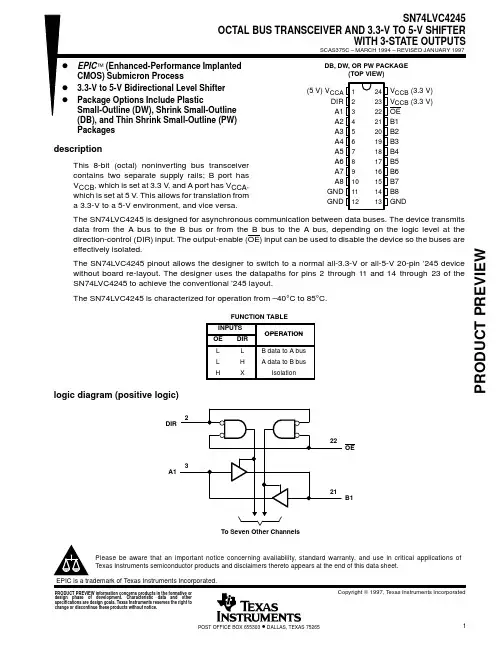
74LVC245A; 74LVCH245AOctal bus transceiver; 3-stateRev. 9 — 11 September 2018Product data sheet1. General descriptionThe 74LVC245A; 74LVCH245A are 8-bit transceivers featuring non-inverting 3-state buscompatible outputs in both send and receive directions. The device features an output enable(OE) input for easy cascading and a send/receive (DIR) input for direction control. OE controls theoutputs so that the buses are effectively isolated.Inputs can be driven from either 3.3 V or 5 V devices. When disabled, up to 5.5 V can be applied tothe outputs. These features allow the use of these devices in mixed 3.3 V and 5 V applications.The 74LVCH245A bus hold on data inputs eliminates the need for external pull-up resistors to holdunused inputs.2. Features and benefits• 5 V tolerant inputs/outputs for interfacing with 5 V logic•Wide supply voltage range from 1.2 V to 3.6 V•CMOS low-power consumption•Direct interface with TTL levels•Inputs accept voltages up to 5.5 V•High-impedance when V CC = 0 V•Bus hold on all data inputs (74LVCH245A only)•Complies with JEDEC standard:•JESD8-7A (1.65 V to 1.95 V)•JESD8-5A (2.3 V to 2.7 V)•JESD8-C/JESD36 (2.7 V to 3.6 V)•ESD protection:•HBM JESD22-A114F exceeds 2000 V•MM JESD22-A115B exceeds 200 V•CDM JESD22-C101E exceeds 1000 V•Specified from -40 °C to +85 °C and -40 °C to +125 °C3. Ordering information4. Functional diagram5. Pinning information5.1. Pinning74LVC245A 74LVCH245ADIR V CC A0OE A1B0A2B1A3B2A4B3A5B4A6B5A7B6GND B7001aak2921234567891012111413161518172019Fig. 3.Pin configuration SOT163-1 (SO20),SOT339-1 (SSOP20) and SOT360-1 (TSSOP20)001aak29374LVC245A 74LVCH245AT ransparent top viewB6A6A7B5A5B4A4B3A3B2A2B1A1B0A0OE G N D B 7D I R V C C9128137146155164173182191011120terminal 1 index areaGND (1)(1) This is not a supply pin. The substrate is attached to this pad using conductive die attach material. There is no electrical or mechanical requirement to solder this pad. However, if it is soldered, the solder land should remain floating or be connected to GND.Fig. 4.Pin configuration SOT764-1 (DHVQFN20)5.2. Pin description6. Functional descriptionTable 3. Function selectionH = HIGH voltage level; L = LOW voltage level; X = don’t care; Z = high impedance OFF-state.7. Limiting valuesTable 4. Limiting valuesIn accordance with the Absolute Maximum Rating System (IEC 60134). Voltages are referenced to GND (ground = 0 V).[1]The minimum input voltage ratings may be exceeded if the input current ratings are observed.[2]The output voltage ratings may be exceeded if the output current ratings are observed.[3]For SO20 packages: above 70 °C derate linearly with 8 mW/K.For (T)SSOP20 packages: above 60 °C derate linearly with 5.5 mW/K.For DHVQFN20 packages: above 60 °C derate linearly with 4.5 mW/K.8. Recommended operating conditions9. Static characteristicsTable 6. Static characteristicsAt recommended operating conditions. Voltages are referenced to GND (ground = 0 V).[1]All typical values are measured at V CC = 3.3 V (unless stated otherwise) and T amb = 25 °C.[2]The bus hold circuit is switched off when V I ˃ V CC allowing 5.5 V on the input terminal.[3]For I/O ports the parameter I OZ includes the input leakage current.[4]Valid for data inputs of bus hold parts only (74LVCH245A). Note that control inputs do not have a bus hold circuit.[5]The specified sustaining current at the data input holds the input below the specified V I level.[6]The specified overdrive current at the data input forces the data input to the opposite input state.10. Dynamic characteristicsTable 7. Dynamic characteristicsVoltages are referenced to GND (ground = 0 V). For test circuit see Fig. 7.[1]Typical values are measured at T amb = 25 °C and V CC = 1.2 V, 1.8 V, 2.5 V, 2.7 V and 3.3 V respectively.[2]t pd is the same as t PLH and t PHL.t en is the same as t PZL and t PZH.t dis is the same as t PLZ and t PHZ.[3]Skew between any two outputs of the same package switching in the same direction. This parameter is guaranteed by design.[4]C PD is used to determine the dynamic power dissipation (P D in μW).P D = C PD × V CC2 × f i × N + Σ(C L × V CC2 × f o) where:f i = input frequency in MHz; f o = output frequency in MHzC L = output load capacitance in pFV CC = supply voltage in VoltsN = number of inputs switchingΣ(C L × V CC2 × f o) = sum of the outputs.10.1. Waveforms and test circuit11. Package outlineSO20: plastic small outline package; 20 leads; body width 7.5 mm SOT163-1Fig. 8.Package outline SOT163-1 (SO20)SSOP20: plastic shrink small outline package; 20 leads; body width 5.3 mm SOT339-1Fig. 9.Package outline SOT339-1 (SSOP20)TSSOP20: plastic thin shrink small outline package; 20 leads; body width 4.4 mm SOT360-1Fig. 10.Package outline SOT360-1 (TSSOP20)DHVQFN20: plastic dual in-line compatible thermal enhanced very thin quad flat package; no leads;Fig. 11.Package outline SOT764-1 (DHVQFN20)12. Abbreviations13. Revision history14. Legal informationData sheet status[1]Please consult the most recently issued document before initiating orcompleting a design.[2]The term 'short data sheet' is explained in section "Definitions".[3]The product status of device(s) described in this document may havechanged since this document was published and may differ in case ofmultiple devices. The latest product status information is available onthe internet at https://.DefinitionsDraft — The document is a draft version only. The content is still under internal review and subject to formal approval, which may result in modifications or additions. Nexperia does not give any representations or warranties as to the accuracy or completeness of information included herein and shall have no liability for the consequences of use of such information. Short data sheet — A short data sheet is an extract from a full data sheet with the same product type number(s) and title. A short data sheet is intended for quick reference only and should not be relied upon to contain detailed and full information. For detailed and full information see the relevant full data sheet, which is available on request via the local Nexperia sales office. In case of any inconsistency or conflict with the short data sheet, the full data sheet shall prevail.Product specification — The information and data provided in a Product data sheet shall define the specification of the product as agreed between Nexperia and its customer, unless Nexperia and customer have explicitly agreed otherwise in writing. In no event however, shall an agreement be valid in which the Nexperia product is deemed to offer functions and qualities beyond those described in the Product data sheet.DisclaimersLimited warranty and liability — Information in this document is believedto be accurate and reliable. However, Nexperia does not give any representations or warranties, expressed or implied, as to the accuracyor completeness of such information and shall have no liability for the consequences of use of such information. Nexperia takes no responsibility for the content in this document if provided by an information source outside of Nexperia.In no event shall Nexperia be liable for any indirect, incidental, punitive, special or consequential damages (including - without limitation - lost profits, lost savings, business interruption, costs related to the removalor replacement of any products or rework charges) whether or not such damages are based on tort (including negligence), warranty, breach of contract or any other legal theory.Notwithstanding any damages that customer might incur for any reason whatsoever, Nexperia’s aggregate and cumulative liability towards customer for the products described herein shall be limited in accordance with the Terms and conditions of commercial sale of Nexperia.Right to make changes — Nexperia reserves the right to make changesto information published in this document, including without limitation specifications and product descriptions, at any time and without notice. This document supersedes and replaces all information supplied prior to the publication hereof.Suitability for use — Nexperia products are not designed, authorized or warranted to be suitable for use in life support, life-critical or safety-critical systems or equipment, nor in applications where failure or malfunctionof an Nexperia product can reasonably be expected to result in personal injury, death or severe property or environmental damage. Nexperia and its suppliers accept no liability for inclusion and/or use of Nexperia products in such equipment or applications and therefore such inclusion and/or use is at the customer’s own risk.Quick reference data — The Quick reference data is an extract of the product data given in the Limiting values and Characteristics sections of this document, and as such is not complete, exhaustive or legally binding. Applications — Applications that are described herein for any of these products are for illustrative purposes only. Nexperia makes no representation or warranty that such applications will be suitable for the specified use without further testing or modification.Customers are responsible for the design and operation of their applications and products using Nexperia products, and Nexperia accepts no liability for any assistance with applications or customer product design. It is customer’s sole responsibility to determine whether the Nexperia product is suitableand fit for the customer’s applications and products planned, as well asfor the planned application and use of customer’s third party customer(s). Customers should provide appropriate design and operating safeguards to minimize the risks associated with their applications and products. Nexperia does not accept any liability related to any default, damage, costs or problem which is based on any weakness or default in the customer’s applications or products, or the application or use by customer’s third party customer(s). Customer is responsible for doing all necessary testing for the customer’s applications and products using Nexperia products in order to avoid a default of the applications and the products or of the application or use by customer’s third party customer(s). Nexperia does not accept any liability in this respect.Limiting values — Stress above one or more limiting values (as defined in the Absolute Maximum Ratings System of IEC 60134) will cause permanent damage to the device. Limiting values are stress ratings only and (proper) operation of the device at these or any other conditions above thosegiven in the Recommended operating conditions section (if present) or the Characteristics sections of this document is not warranted. Constant or repeated exposure to limiting values will permanently and irreversibly affect the quality and reliability of the device.Terms and conditions of commercial sale — Nexperia products aresold subject to the general terms and conditions of commercial sale, as published at /profile/terms, unless otherwise agreed in a valid written individual agreement. In case an individual agreement is concluded only the terms and conditions of the respective agreement shall apply. Nexperia hereby expressly objects to applying the customer’s general terms and conditions with regard to the purchase of Nexperia products by customer.No offer to sell or license — Nothing in this document may be interpreted or construed as an offer to sell products that is open for acceptance or the grant, conveyance or implication of any license under any copyrights, patents or other industrial or intellectual property rights.Export control — This document as well as the item(s) described herein may be subject to export control regulations. Export might require a prior authorization from competent authorities.Non-automotive qualified products — Unless this data sheet expressly states that this specific Nexperia product is automotive qualified, the product is not suitable for automotive use. It is neither qualified nor tested in accordance with automotive testing or application requirements. Nexperia accepts no liability for inclusion and/or use of non-automotive qualified products in automotive equipment or applications.In the event that customer uses the product for design-in and use in automotive applications to automotive specifications and standards, customer (a) shall use the product without Nexperia’s warranty of the product for such automotive applications, use and specifications, and (b) whenever customer uses the product for automotive applications beyond Nexperia’s specifications such use shall be solely at customer’s own risk, and (c) customer fully indemnifies Nexperia for any liability, damages or failed product claims resulting from customer design and use of the product for automotive applications beyond Nexperia’s standard warranty and Nexperia’s product specifications.Translations — A non-English (translated) version of a document is for reference only. The English version shall prevail in case of any discrepancy between the translated and English versions.TrademarksNotice: All referenced brands, product names, service names and trademarks are the property of their respective owners.Contents1. General description (1)2. Features and benefits (1)3. Ordering information (2)4. Functional diagram (2)5. Pinning information (3)5.1. Pinning (3)5.2. Pin description (3)6. Functional description (3)7. Limiting values (4)8. Recommended operating conditions (4)9. Static characteristics (5)10. Dynamic characteristics (7)10.1. Waveforms and test circuit (8)11. Package outline (10)12. Abbreviations (14)13. Revision history (14)14. Legal information (15)© Nexperia B.V. 2018. All rights reservedFor more information, please visit: Forsalesofficeaddresses,pleasesendanemailto:*************************** Date of release: 11 September 2018Mouser ElectronicsAuthorized DistributorClick to View Pricing, Inventory, Delivery & Lifecycle Information:N experia:74LVC245AD74LVCH245AD74LVCH245ADB74LVCH245APW74LVC245APW74LVC245ABQ,115 74LVC245AD,11274LVC245ADB,11274LVC245ADB,11874LVC245AD,11874LVC245APW,11274LVC245APW,11874LVCH245ABQ,11574LVCH245AD,11274LVCH245ADB,11274LVCH245ADB,118 74LVCH245AD,11874LVCH245APW,11274LVCH245APW,11874LVC245ABX,11574LVCH245ABX,115 74LVCH245APW/AUJ74LVC245APW/AUJ。
关于驱动芯片国产化替代方案研究发布时间:2022-01-12T02:58:04.070Z 来源:《现代电信科技》2021年第13期作者:邹宇[导读] 随着电子元器件的要求不断提高,但进口元器件存在国外禁运,停产断档的问题,还存在多种安全风险、质量与可靠性隐患及自主保障问题,为提升自主可控能力,必须寻求国产化替代。
(航天风华精密设备有限公司)摘要:面对芯片短缺给智能产业带来的影响,芯片国产化替代步伐也在不断加快。
本文从军用电子元器件国产化需求出发,并对 2 种驱动芯片为具体案例,给出国产化替代的方案,对该国产化驱动芯片进行分析,可确定为该国产化驱动芯片可功能替代进口驱动芯片。
1 引言随着电子元器件的要求不断提高,但进口元器件存在国外禁运,停产断档的问题,还存在多种安全风险、质量与可靠性隐患及自主保障问题,为提升自主可控能力,必须寻求国产化替代。
2 芯片简介本文对 SN74LVC4245APWR、SN74LVC573ADB 两种驱动芯片进行具体分析,该芯片为美国德州仪器生产,本文拟采用北京华芯微生产的 HRLVC4245M、HRALS573M 进行替代,并从电气参数、外形封装、管脚定义、质量等级、环境使用能力等方面进行分析比较。
2.1 驱动芯片 SN74LVC4245APWR 国产化替代方案SN74LVC4245APWR 是三态电平转换驱动器芯片,具有三态输出功能,实现双向的 8 位数据传输及电平转换功能,并可 3.3V 和5.0V 信号的转换。
该芯片主要用于连接串口控制器和光耦以及驱动芯片 174 之间进行电压转换,其具体电路见图 1。
图 1 SN74LVC4245APWR 的电路应用拟采用北京华芯微生产的 HRLVC4245M 进行替换。
该器件质量保证等级为 B 级,封装形式为 CSOP24 陶瓷封装。
原进口器件与拟替代的国产器件主要参数对比见表 1 所示。
表 1 SN74LVC4245APWR 和 HRLVC4245M 参数对比表对表 1 中各项参数对比可知,二者电特性参数相同,HRLVC4245M 工作温度范围大于原进口器件,二者封装形式不同,不能直接实现拔插替换,需更改原电路原理及印制板封装。
FEATURESDESCRIPTION/ORDERING INFORMATIONDB, DW, OR PW PACKAGE(TOP VIEW)123456789101112242322212019181716151413(5 V) V CCADIRA1A2A3A4A5A6A7A8GNDGNDV CCB (3.3 V)V CCB (3.3 V)OEB1B2B3B4B5B6B7B8GNDSN74LVC4245AOCTAL BUS TRANSCEIVER AND3.3-V TO5-V SHIFTERWITH3-STATE OUTPUTSSCAS375H–MARCH1994–REVISED MARCH2005•Bidirectional Voltage Translator• 5.5V on A Port and2.7V to3.6V on B Port•Control Inputs V IH/V IL Levels Are Referencedto V CCA Voltage•Latch-Up Performance Exceeds250mA PerJESD17•ESD Protection Exceeds JESD22–2000-V Human-Body Model(A114-A)–200-V Machine Model(A115-A)–1000-V Charged-Device Model(C101)This8-bit(octal)noninverting bus transceivercontains two separate supply rails;B port has V CCB,which is set at3.3V,and A port has V CCA,which isset at5V.This allows for translation from a3.3-V toa5-V environment,and vice versa.The SN74LVC4245A is designed for asynchronous communication between data buses.The device transmits data from the A bus to the B bus or from the B bus to the A bus,depending on the logic level at the direction-control(DIR)input.The output-enable(OE)input can be used to disable the device so the buses are effectively isolated.The control circuitry(DIR,OE)is powered by V CCA.The SN74LVC4245A pinout allows the designer to switch to a normal all-3.3-V or all-5-V20-pin'245device without board re-layout.The designer uses the data paths for pins2–11and14–23of the SN74LVC4245A to align with the conventional'245pinout.ORDERING INFORMATIONT A PACKAGE(1)ORDERABLE PART NUMBER TOP-SIDE MARKINGTube of25SN74LVC4245ADWSOIC–DW LVC4245AReel of2000SN74LVC4245ADWRSSOP–DB Reel of2000SN74LVC4245ADBR LJ245A–40°C to85°CTube of60SN74LVC4245APWTSSOP–PW Reel of2000SN74LVC4245APWR LJ245AReel of250SN74LVC4245APWT(1)Package drawings,standard packing quantities,thermal data,symbolization,and PCB design guidelines are available at/sc/package.FUNCTION TABLEINPUTSOPERATIONOE DIRL L B data to A busL H A data to B busH X IsolationPlease be aware that an important notice concerning availability,standard warranty,and use in critical applications of TexasInstruments semiconductor products and disclaimers thereto appears at the end of this data sheet.PRODUCTION DATA information is current as of publication date.Copyright©1994–2005,Texas Instruments Incorporated Products conform to specifications per the terms of the TexasInstruments standard warranty.Production processing does notnecessarily include testing of all parameters.DIROEA1B1To Seven Other ChannelsAbsolute Maximum Ratings (1)SN74LVC4245AOCTAL BUS TRANSCEIVER AND 3.3-V TO 5-V SHIFTER WITH 3-STATE OUTPUTSSCAS375H–MARCH 1994–REVISED MARCH 2005LOGIC DIAGRAM (POSITIVE LOGIC)over operating free-air temperature range for V CCA =4.5V to 5.5V (unless otherwise noted)MINMAX UNIT V CCA Supply voltage range –0.5 6.5V A port (2)–0.5V CCA +0.5V I Input voltage range V Control inputs –0.56V O Output voltage range A port (2)–0.5V CCA +0.5V I IK Input clamp current V I <0–50mA I OK Output clamp current V O <0–50mA I OContinuous output current±50mA Continuous current through each V CCA or GND±100mADB package63θJA Package thermal impedance (3)DW package 46°C/W PW package88T stg Storage temperature range–65150°C (1)Stresses beyond those listed under "absolute maximum ratings"may cause permanent damage to the device.These are stress ratings only,and functional operation of the device at these or any other conditions beyond those indicated under "recommended operating conditions"is not implied.Exposure to absolute-maximum-rated conditions for extended periods may affect device reliability.(2)This value is limited to 6V maximum.(3)The package thermal impedance is calculated in accordance with JESD 51-7.2Absolute Maximum Ratings(1) Recommended Operating Conditions(1) Recommended Operating Conditions(1)SN74LVC4245A OCTAL BUS TRANSCEIVER AND3.3-V TO5-V SHIFTERWITH3-STATE OUTPUTSSCAS375H–MARCH1994–REVISED MARCH2005over operating free-air temperature range for VCCB=2.7V to3.6V(unless otherwise noted)MIN MAX UNITV CCB Supply voltage range–0.5 4.6VV I Input voltage range B port(2)–0.5V CCB+0.5VV O Output voltage range B port(2)–0.5V CCB+0.5VI IK Input clamp current V I<0–50mAI OK Output clamp current V O<0–50mAI O Continuous output current±50mAContinuous current through V CCB or GND±100mADB package63θJA Package thermal impedance(3)DW package46°C/WPW package88T stg Storage temperature range–65150°C (1)Stresses beyond those listed under"absolute maximum ratings"may cause permanent damage to the device.These are stress ratingsonly,and functional operation of the device at these or any other conditions beyond those indicated under"recommended operating conditions"is not implied.Exposure to absolute-maximum-rated conditions for extended periods may affect device reliability.(2)This value is limited to4.6V maximum.(3)The package thermal impedance is calculated in accordance with JESD51-7.for VCCA=4.5V to5.5VMIN MAX UNITV CCA Supply voltage 4.5 5.5VV IH High-level input voltage2VV IL Low-level input voltage0.8VV IA Input voltage0V CCA VV OA Output voltage0V CCA VI OH High-level output current–24mAI OL Low-level output current24mAT A Operating free-air temperature–4085°C (1)All unused inputs of the device must be held at the associated V CC or GND to ensure proper device operation.Refer to the TIapplication report,Implications of Slow or Floating CMOS Inputs,literature number SCBA004.for VCCB=2.7V to3.6VMIN MAX UNITV CCB Supply voltage 2.7 3.6VV IH High-level input voltage V CCB=2.7V to3.6V2VV IL Low-level input voltage V CCB=2.7V to3.6V0.8VV IB Input voltage0V CCB VV OB Output voltage0V CCB VV CCB=2.7V–12I OH High-level output current mAV CCB=3V–24V CCB=2.7V12I OL Low-level output current mAV CCB=3V24T A Operating free-air temperature–4085°C (1)All unused inputs of the device must be held at the associated V CC or GND to ensure proper device operation.Refer to the TIapplication report,Implications of Slow or Floating CMOS Inputs,literature number SCBA004.3Electrical Characteristics (1)Electrical Characteristics (1)SN74LVC4245AOCTAL BUS TRANSCEIVER AND 3.3-V TO 5-V SHIFTER WITH 3-STATE OUTPUTSSCAS375H–MARCH 1994–REVISED MARCH 2005over recommended operating free-air temperature range for V CCA =4.5V to 5.5V (unless otherwise noted)PARAMETERTEST CONDITIONSV CCA MIN TYP (2)MAXUNIT4.5V 4.3I OH =–100µA5.5V 5.3V OHV4.5V 3.7I OH =–24mA5.5V 4.74.5V 0.2I OL =100µA5.5V 0.2V OLV 4.5V 0.55I OL =24mA5.5V 0.55I I Control inputs V I =V CCA or GND 5.5V ±1µA I OZ (3)A portV O =V CCA or GND 5.5V ±5µA I CCA V I =V CCA or GND,I O =05.5V 80µA ∆I CCA (4)One input at 3.4V,Other inputs at V CCA or GND5.5V 1.5mA C i Control inputs V I =V CCA or GND Open 5pF C io A port V O =V CCA or GND5V11pF (1)V CCB =2.7V to 3.6V(2)All typical values are measured at V CC =5V,T A =25°C.(3)For I/O ports,the parameter I OZ includes the input leakage current.(4)This is the increase in supply current for each input that is at one of the specified TTL voltage levels,rather than 0V or the associated V CC .over recommended operating free-air temperature range for V CCB =2.7V to 3.6V (unless otherwise noted)PARAMETERTEST CONDITIONSV CCB MIN TYP (2)MAXUNITI OH =–100µA2.7V to3.6V V CC –0.22.7V 2.2V OHI OH =–12mA V3V 2.4I OH =–24mA 3V 2I OL =100µA2.7V to3.6V0.2V OL I OL =12mA 2.7V 0.4VI OL =24mA 3V 0.55I OZ (3)B portV O =V CCB or GND 3.6V ±5µA I CCB V I =V CCB or GND,I O =03.6V 50µA ∆I CCB (4)One input at V CCB –0.6V,Other inputs at V CCB or GND2.7V to3.6V0.5mA C io B port V O =V CCB or GND3.3V11pF (1)V CCA =5V ±0.5V(2)All typical values are measured at V CC =3.3V,T A =25°C.(3)For I/O ports,the parameter I OZ includes the input leakage current.(4)This is the increase in supply current for each input that is at one of the specified TTL voltage levels,rather than 0V or the associated V CC .4Switching CharacteristicsOperating Characteristics Power-Up Considerations(1)SN74LVC4245A OCTAL BUS TRANSCEIVER AND3.3-V TO5-V SHIFTERWITH3-STATE OUTPUTSSCAS375H–MARCH1994–REVISED MARCH2005over recommended operating free-air temperature range,CL=50pF(unless otherwise noted)(see Figure1and Figure2)V CCA=5V±0.5V,FROM TO VCCB =2.7V to3.6VPARAMETER UNIT(INPUT)(OUTPUT)MIN MAXt PHL1 6.3A B nst PLH1 6.7t PHL1 6.1B A nst PLH15t PZL19OE A ns t PZH18.1t PZL18.8OE B ns t PZH19.8t PLZ17OE A ns t PHZ1 5.8t PLZ17.7OE B ns t PHZ17.8V CCA =4.5V to5.5V,VCCB=2.7V to3.6V,TA=25°CPARAMETER TEST CONDITIONS TYP UNITOutputs enabled39.5C pd Power dissipation capacitance per transceiver C L=0,f=10MHz pFOutputs disabled5TI level-translation devices offer an opportunity for successful mixed-voltage signal design.A proper power-up sequence always should be followed to avoid excessive supply current,bus contention,oscillations,or other anomalies caused by improperly biased device pins.Take these precautions to guard against such power-up problems:1.Connect ground before any supply voltage is applied.2.Power up the control side of the device(V CCA for all four of these devices).3.Tie OE to V CCA with a pullup resistor so that it ramps with V CCA.4.Depending on the direction of the data path,DIR can be high or low.If DIR high is needed(A data to B bus),ramp it with V CCA.Otherwise,keep DIR low.(1)Refer to the TI application report,Texas Instruments Voltage-Level-Translation Devices,literature number SCEA021.5PARAMETER MEASUREMENT INFORMATIONFrom Output Under TestC LLOAD CIRCUIT × V CCOpen VOLTAGE WAVEFORMS PROPAGATION DELAY TIMES NONINVERTING OUTPUTSV OHVOLOutput ControlOutput Waveform 1S1 at 2 × V CC(see Note B)Output Waveform 2S1 at GND (see Note B)V OLV OH V CC0 V≈0 V3 VVOLTAGE WAVEFORMS ENABLE AND DISABLE TIMES LOW- AND HIGH-LEVEL ENABLINGOutputt PLH /t PHL t PLZ /t PZL t PHZ /t PZHOpen 2 × V CC GNDTEST S1NOTES: A.C L includes probe and jig capacitance.B.Waveform 1 is for an output with internal conditions such that the output is low, except when disabled by the output control.Waveform 2 is for an output with internal conditions such that the output is high, except when disabled by the output control.C.All input pulses are supplied by generators having the following characteristics: PRR ≤ 10 MHz, Z O = 50 Ω, t r ≤ 2.5 ns, t f ≤ 2.5 ns.D.The outputs are measured one at a time, with one transition per measurement.E.All parameters and waveforms are not applicable to all devices.V CC0 V InputV CC0 VInputVOLTAGE WAVEFORMS PULSE DURATIONSN74LVC4245AOCTAL BUS TRANSCEIVER AND 3.3-V TO 5-V SHIFTER WITH 3-STATE OUTPUTSSCAS375H–MARCH 1994–REVISED MARCH 2005A PORTFigure 1.Load Circuit and Voltage Waveforms6PARAMETER MEASUREMENT INFORMATIONFrom Output Under TestC LLOAD CIRCUIT Open VOLTAGE WAVEFORMS PROPAGATION DELAY TIMES NONINVERTING OUTPUTSV OHV OLOutput ControlOutput Waveform 1S1 at 7 V (see Note B)Output Waveform 2S1 at GND (see Note B)V OLV OH 3.5 V0 V≈0 V3 VVOLTAGE WAVEFORMS ENABLE AND DISABLE TIMES LOW- AND HIGH-LEVEL ENABLINGOutputt PLH /t PHL t PLZ /t PZL t PHZ /t PZHOpen 7 V GNDTEST S1NOTES: A.C L includes probe and jig capacitance.B.Waveform 1 is for an output with internal conditions such that the output is low, except when disabled by the output control.Waveform 2 is for an output with internal conditions such that the output is high, except when disabled by the output control.C.All input pulses are supplied by generators having the following characteristics: PRR ≤ 10 MHz, Z O = 50 Ω, t r ≤ 2.5 ns, t f ≤ 2.5 ns.D.The outputs are measured one at a time, with one transition per measurement.E.All parameters and waveforms are not applicable to all devices.3 V0 V Input3 V0 VInputVOLTAGE WAVEFORMS PULSE DURATIONSN74LVC4245AOCTAL BUS TRANSCEIVER AND 3.3-V TO 5-V SHIFTERWITH 3-STATE OUTPUTSSCAS375H–MARCH 1994–REVISED MARCH 2005B PORTFigure 2.Load Circuit and Voltage Waveforms7PACKAGING INFORMATIONOrderable Device Status (1)Package Type PackageDrawing Pins Package Qty Eco Plan (2)Lead/Ball FinishMSL Peak Temp (3)Samples(Requires Login)SN74LVC4245ADBR ACTIVE SSOP DB242000Green (RoHS& no Sb/Br)CU NIPDAU Level-1-260C-UNLIMSN74LVC4245ADBRE4ACTIVE SSOP DB242000Green (RoHS& no Sb/Br)CU NIPDAU Level-1-260C-UNLIMSN74LVC4245ADBRG4ACTIVE SSOP DB242000Green (RoHS& no Sb/Br)CU NIPDAU Level-1-260C-UNLIMSN74LVC4245ADW ACTIVE SOIC DW2425Green (RoHS& no Sb/Br)CU NIPDAU Level-1-260C-UNLIM SN74LVC4245ADWE4ACTIVE SOIC DW2425TBD Call TI Call TISN74LVC4245ADWG4ACTIVE SOIC DW2425TBD Call TI Call TISN74LVC4245ADWR ACTIVE SOIC DW242000Green (RoHS& no Sb/Br)CU NIPDAU Level-1-260C-UNLIMSN74LVC4245ADWRE4ACTIVE SOIC DW242000Green (RoHS& no Sb/Br)CU NIPDAU Level-1-260C-UNLIMSN74LVC4245ADWRG4ACTIVE SOIC DW242000Green (RoHS& no Sb/Br)CU NIPDAU Level-1-260C-UNLIMSN74LVC4245APW ACTIVE TSSOP PW2460Green (RoHS& no Sb/Br)CU NIPDAU Level-1-260C-UNLIMSN74LVC4245APWE4ACTIVE TSSOP PW2460Green (RoHS& no Sb/Br)CU NIPDAU Level-1-260C-UNLIMSN74LVC4245APWG4ACTIVE TSSOP PW2460Green (RoHS& no Sb/Br)CU NIPDAU Level-1-260C-UNLIMSN74LVC4245APWR ACTIVE TSSOP PW242000Green (RoHS& no Sb/Br)CU NIPDAU Level-1-260C-UNLIMSN74LVC4245APWRE4ACTIVE TSSOP PW242000Green (RoHS& no Sb/Br)CU NIPDAU Level-1-260C-UNLIMSN74LVC4245APWRG4ACTIVE TSSOP PW242000Green (RoHS& no Sb/Br)CU NIPDAU Level-1-260C-UNLIMSN74LVC4245APWT ACTIVE TSSOP PW24250Green (RoHS& no Sb/Br)CU NIPDAU Level-1-260C-UNLIMSN74LVC4245APWTE4ACTIVE TSSOP PW24250Green (RoHS& no Sb/Br)CU NIPDAU Level-1-260C-UNLIMSN74LVC4245APWTG4ACTIVE TSSOP PW24250Green (RoHS& no Sb/Br)CU NIPDAU Level-1-260C-UNLIMAddendum-Page 1(1) The marketing status values are defined as follows:ACTIVE: Product device recommended for new designs.LIFEBUY: TI has announced that the device will be discontinued, and a lifetime-buy period is in effect.NRND: Not recommended for new designs. Device is in production to support existing customers, but TI does not recommend using this part in a new design.PREVIEW: Device has been announced but is not in production. Samples may or may not be available.OBSOLETE: TI has discontinued the production of the device.(2) Eco Plan - The planned eco-friendly classification: Pb-Free (RoHS), Pb-Free (RoHS Exempt), or Green (RoHS & no Sb/Br) - please check /productcontent for the latest availability information and additional product content details.TBD: The Pb-Free/Green conversion plan has not been defined.Pb-Free (RoHS): TI's terms "Lead-Free" or "Pb-Free" mean semiconductor products that are compatible with the current RoHS requirements for all 6 substances, including the requirement that lead not exceed 0.1% by weight in homogeneous materials. Where designed to be soldered at high temperatures, TI Pb-Free products are suitable for use in specified lead-free processes.Pb-Free (RoHS Exempt): This component has a RoHS exemption for either 1) lead-based flip-chip solder bumps used between the die and package, or 2) lead-based die adhesive used between the die and leadframe. The component is otherwise considered Pb-Free (RoHS compatible) as defined above.Green (RoHS & no Sb/Br): TI defines "Green" to mean Pb-Free (RoHS compatible), and free of Bromine (Br) and Antimony (Sb) based flame retardants (Br or Sb do not exceed 0.1% by weight in homogeneous material)(3) MSL, Peak Temp. -- The Moisture Sensitivity Level rating according to the JEDEC industry standard classifications, and peak solder temperature.Important Information and Disclaimer:The information provided on this page represents TI's knowledge and belief as of the date that it is provided. TI bases its knowledge and belief on information provided by third parties, and makes no representation or warranty as to the accuracy of such information. Efforts are underway to better integrate information from third parties. TI has taken and continues to take reasonable steps to provide representative and accurate information but may not have conducted destructive testing or chemical analysis on incoming materials and chemicals. TI and TI suppliers consider certain information to be proprietary, and thus CAS numbers and other limited information may not be available for release.In no event shall TI's liability arising out of such information exceed the total purchase price of the TI part(s) at issue in this document sold by TI to Customer on an annual basis.OTHER QUALIFIED VERSIONS OF SN74LVC4245A :•Enhanced Product: SN74LVC4245A-EPNOTE: Qualified Version Definitions:•Enhanced Product - Supports Defense, Aerospace and Medical ApplicationsAddendum-Page 2TAPE AND REELINFORMATION*All dimensionsare nominalDevicePackage Type Package Drawing Pins SPQReel Diameter (mm)Reel Width W1(mm)A0(mm)B0(mm)K0(mm)P1(mm)W (mm)Pin1Quadrant SN74LVC4245ADBR SSOP DB 242000330.016.48.28.8 2.512.016.0Q1SN74LVC4245ADWR SOIC DW 242000330.024.410.7515.7 2.712.024.0Q1SN74LVC4245APWR TSSOP PW 242000330.016.4 6.958.3 1.68.016.0Q1SN74LVC4245APWTTSSOPPW24250330.016.46.958.31.68.016.0Q1PACKAGE MATERIALS INFORMATION28-Jan-2012Pack Materials-Page 1*All dimensionsare nominal DevicePackage Type Package Drawing Pins SPQ Length (mm)Width (mm)Height (mm)SN74LVC4245ADBRSSOP DB 242000346.0346.033.0SN74LVC4245ADWRSOIC DW 242000346.0346.041.0SN74LVC4245APWRTSSOP PW 242000346.0346.033.0SN74LVC4245APWT TSSOP PW 24250346.0346.033.0PACKAGE MATERIALS INFORMATION 28-Jan-2012Pack Materials-Page 2IMPORTANT NOTICETexas Instruments Incorporated and its subsidiaries(TI)reserve the right to make corrections,modifications,enhancements,improvements, and other changes to its products and services at any time and to discontinue any product or service without notice.Customers should obtain the latest relevant information before placing orders and should verify that such information is current and complete.All products are sold subject to TI’s terms and conditions of sale supplied at the time of order acknowledgment.TI warrants performance of its hardware products to the specifications applicable at the time of sale in accordance with TI’s standard warranty.Testing and other quality control techniques are used to the extent TI deems necessary to support this warranty.Except where mandated by government requirements,testing of all parameters of each product is not necessarily performed.TI assumes no liability for applications assistance or customer product design.Customers are responsible for their products and applications using TI components.To minimize the risks associated with customer products and applications,customers should provide adequate design and operating safeguards.TI does not warrant or represent that any license,either express or implied,is granted under any TI patent right,copyright,mask work right, or other TI intellectual property right relating to any combination,machine,or process in which TI products or services are rmation published by TI regarding third-party products or services does not constitute a license from TI to use such products or services or a warranty or endorsement e of such information may require a license from a third party under the patents or other intellectual property of the third party,or a license from TI under the patents or other intellectual property of TI.Reproduction of TI information in TI data books or data sheets is permissible only if reproduction is without alteration and is accompanied by all associated warranties,conditions,limitations,and notices.Reproduction of this information with alteration is an unfair and deceptive business practice.TI is not responsible or liable for such altered rmation of third parties may be subject to additional restrictions.Resale of TI products or services with statements different from or beyond the parameters stated by TI for that product or service voids all express and any implied warranties for the associated TI product or service and is an unfair and deceptive business practice.TI is not responsible or liable for any such statements.TI products are not authorized for use in safety-critical applications(such as life support)where a failure of the TI product would reasonably be expected to cause severe personal injury or death,unless officers of the parties have executed an agreement specifically governing such use.Buyers represent that they have all necessary expertise in the safety and regulatory ramifications of their applications,and acknowledge and agree that they are solely responsible for all legal,regulatory and safety-related requirements concerning their products and any use of TI products in such safety-critical applications,notwithstanding any applications-related information or support that may be provided by TI.Further,Buyers must fully indemnify TI and its representatives against any damages arising out of the use of TI products in such safety-critical applications.TI products are neither designed nor intended for use in military/aerospace applications or environments unless the TI products are specifically designated by TI as military-grade or"enhanced plastic."Only products designated by TI as military-grade meet military specifications.Buyers acknowledge and agree that any such use of TI products which TI has not designated as military-grade is solely at the Buyer's risk,and that they are solely responsible for compliance with all legal and regulatory requirements in connection with such use. TI products are neither designed nor intended for use in automotive applications or environments unless the specific TI products are designated by TI as compliant with ISO/TS16949requirements.Buyers acknowledge and agree that,if they use any non-designated products in automotive applications,TI will not be responsible for any failure to meet such requirements.Following are URLs where you can obtain information on other Texas Instruments products and application solutions:Products ApplicationsAudio /audio Automotive and Transportation /automotiveAmplifiers Communications and Telecom /communicationsData Converters Computers and Peripherals /computersDLP®Products Consumer Electronics /consumer-appsDSP Energy and Lighting /energyClocks and Timers /clocks Industrial /industrialInterface Medical /medicalLogic Security /securityPower Mgmt Space,Avionics and Defense /space-avionics-defense Microcontrollers Video and Imaging /videoRFID OMAP Mobile Processors /omapWireless Connectivity /wirelessconnectivityTI E2E Community Home Page Mailing Address:Texas Instruments,Post Office Box655303,Dallas,Texas75265Copyright©2012,Texas Instruments Incorporated。
元器件交易网IMPORTANT NOTICETexas Instruments (TI) reserves the right to make changes to its products or to discontinue any semiconductorproduct or service without notice, and advises its customers to obtain the latest version of relevant informationto verify, before placing orders, that the information being relied on is current.TI warrants performance of its semiconductor products and related software to the specifications applicable atthe time of sale in accordance with TI’s standard warranty. Testing and other quality control techniques areutilized to the extent TI deems necessary to support this warranty. Specific testing of all parameters of eachdevice is not necessarily performed, except those mandated by government requirements.Certain applications using semiconductor products may involve potential risks of death, personal injury, orsevere property or environmental damage (“Critical Applications”).TI SEMICONDUCTOR PRODUCTS ARE NOT DESIGNED, INTENDED, AUTHORIZED, OR WARRANTEDTO BE SUITABLE FOR USE IN LIFE-SUPPORT APPLICATIONS, DEVICES OR SYSTEMS OR OTHERCRITICAL APPLICATIONS.Inclusion of TI products in such applications is understood to be fully at the risk of the customer. Use of TIproducts in such applications requires the written approval of an appropriate TI officer. Questions concerningpotential risk applications should be directed to TI through a local SC sales office.In order to minimize risks associated with the customer’s applications, adequate design and operatingsafeguards should be provided by the customer to minimize inherent or procedural hazards.TI assumes no liability for applications assistance, customer product design, software performance, orinfringement of patents or services described herein. Nor does TI warrant or represent that any license, eitherexpress or implied, is granted under any patent right, copyright, mask work right, or other intellectual propertyright of TI covering or relating to any combination, machine, or process in which such semiconductor productsor services might be or are used.Copyright © 1996, Texas Instruments Incorporated。
FEATURESPW PACKAGE(TOP VIEW)123456789101112242322212019181716151413(5 V) V CCADIRA1A2A3A4A5A6A7A8GNDGNDV CCB (3.3 V)V CCB (3.3 V)OEB1B2B3B4B5B6B7B8GND DESCRIPTION/ORDERING INFORMATIONSN74LVC4245A-EPOCTAL BUS TRANSCEIVER AND3.3-V TO5-V SHIFTERWITH3-STATE OUTPUTSSCAS742–DECEMBER2003–REVISED AUGUST2005•Controlled Baseline–One Assembly/Test Site,One FabricationSite•Enhanced Diminishing ManufacturingSources(DMS)Support•Enhanced Product-Change Notification•Qualification Pedigree(1)•Bidirectional Voltage Translator• 5.5V on A Port and2.7V to3.6V on B Port•Latch-Up Performance Exceeds250mA PerJESD17•ESD Protection Exceeds JESD22–2000-V Human-Body Model(A114-A)–200-V Machine Model(A115-A)–1000-V Charged-Device Model(C101)(1)Component qualification in accordance with JEDEC andindustry standards to ensure reliable operation over anextended temperature range.This includes,but is not limitedto,Highly Accelerated Stress Test(HAST)or biased85/85,temperature cycle,autoclave or unbiased HAST,electromigration,bond intermetallic life,and mold compoundlife.Such qualification testing should not be viewed asjustifying use of this component beyond specifiedperformance and environmental limits.This8-bit(octal)noninverting bus transceiver contains two separate supply rails;B port has V CCB,which is set at 3.3V,and A port has V CCA,which is set at5V.This allows for translation from a3.3-V to a5-V environment,and vice versa.The SN74LVC4245A is designed for asynchronous communication between data buses.The device transmits data from the A bus to the B bus or from the B bus to the A bus,depending on the logic level at the direction-control(DIR)input.The output-enable(OE)input can be used to disable the device so the buses are effectively isolated.The SN74LVC4245A pinout allows the designer to switch to a normal all-3.3-V or all-5-V20-pin'245device without board re-layout.The designer uses the data paths for pins2–11and14–23of the SN74LVC4245A to align with the conventional'245pinout.ORDERING INFORMATIONT A PACKAGE(1)ORDERABLE PART NUMBER TOP-SIDE MARKING –40°C to85°C TSSOP–PW Reel of2000SN74LVC4245AIPWREP C4245AEP(1)Package drawings,standard packing quantities,thermal data,symbolization,and PCB design guidelines are available at/sc/package.Please be aware that an important notice concerning availability,standard warranty,and use in critical applications of TexasInstruments semiconductor products and disclaimers thereto appears at the end of this data sheet.PRODUCTION DATA information is current as of publication date.Copyright©2003–2005,Texas Instruments Incorporated Products conform to specifications per the terms of the TexasInstruments standard warranty.Production processing does notnecessarily include testing of all parameters.DIROEA1B1To Seven Other ChannelsSN74LVC4245A-EPOCTAL BUS TRANSCEIVER AND 3.3-V TO 5-V SHIFTER WITH 3-STATE OUTPUTSSCAS742–DECEMBER 2003–REVISED AUGUST 2005FUNCTION TABLEINPUTS OPERATION OE DIR L L B data to A bus L H A data to B busHXIsolationLOGIC DIAGRAM (POSITIVE LOGIC)2Absolute Maximum Ratings(1) Absolute Maximum Ratings(1)SN74LVC4245A-EP OCTAL BUS TRANSCEIVER AND3.3-V TO5-V SHIFTERWITH3-STATE OUTPUTSSCAS742–DECEMBER2003–REVISED AUGUST2005over operating free-air temperature range for VCCA=4.5V to5.5V(unless otherwise noted)MIN MAX UNITV CCA Supply voltage range–0.5 6.5VA port(2)–0.5V CCA+0.5V I Input voltage range VControl inputs–0.56V O Output voltage range A port(2)–0.5V CCA+0.5VI IK Input clamp current V I<0–50mAI OK Output clamp current V O<0–50mAI O Continuous output current±50mAContinuous current through V CCA or GND±100mAθJA Package thermal impedance(3)88°C/WT stg Storage temperature range–65150°C (1)Stresses beyond those listed under"absolute maximum ratings"may cause permanent damage to the device.These are stress ratingsonly,and functional operation of the device at these or any other conditions beyond those indicated under"recommended operating conditions"is not implied.Exposure to absolute-maximum-rated conditions for extended periods may affect device reliability.(2)This value is limited to6V maximum.(3)The package thermal impedance is calculated in accordance with JESD51-7.over operating free-air temperature range for VCCB=2.7V to3.6V(unless otherwise noted)MIN MAX UNITV CCB Supply voltage range–0.5 4.6VV I Input voltage range B port(2)–0.5V CCB+0.5VV O Output voltage range B port(2)–0.5V CCB+0.5VI IK Input clamp current V I<0–50mAI OK Output clamp current V O<0–50mAI O Continuous output current±50mAContinuous current through V CCB or GND±100mAθJA Package thermal impedance(3)88°C/WT stg Storage temperature range–65150°C (1)Stresses beyond those listed under"absolute maximum ratings"may cause permanent damage to the device.These are stress ratingsonly,and functional operation of the device at these or any other conditions beyond those indicated under"recommended operating conditions"is not implied.Exposure to absolute-maximum-rated conditions for extended periods may affect device reliability.(2)This value is limited to4.6V maximum.(3)The package thermal impedance is calculated in accordance with JESD51-7.3Recommended Operating Conditions (1)Recommended Operating Conditions (1)SN74LVC4245A-EPOCTAL BUS TRANSCEIVER AND 3.3-V TO 5-V SHIFTER WITH 3-STATE OUTPUTSSCAS742–DECEMBER 2003–REVISED AUGUST 2005for V CCA =4.5V to 5.5VMINMAX UNIT V CCA Supply voltage 4.5 5.5V V IH High-level input voltage 2V V IL Low-level input voltage 0.8V V I Input voltage 0V CCA V V O Output voltage0V CCA V I OH High-level output current –24mA I OL Low-level output current 24mA T A Operating free-air temperature–4085°C(1)All unused inputs of the device must be held at the associated V CC or GND to ensure proper device operation.Refer to the TI application report,Implications of Slow or Floating CMOS Inputs ,literature number SCBA004.for V CCB =2.7V to 3.6VMINMAX UNIT V CCB Supply voltage 2.7 3.6V V IH High-level input voltage V CCB =2.7V to 3.6V 2V V IL Low-level input voltage V CCB =2.7V to 3.6V0.8V V I Input voltage 0V CCB V V O Output voltage0V CCB V V CCB =2.7V –12I OH High-level output current mA V CCB =3V –24V CCB =2.7V 12I OL Low-level output current mA V CCB =3V24T A Operating free-air temperature–4085°C(1)All unused inputs of the device must be held at the associated V CC or GND to ensure proper device operation.Refer to the TI application report,Implications of Slow or Floating CMOS Inputs ,literature number SCBA004.4Electrical Characteristics(1) Electrical Characteristics(1)SN74LVC4245A-EP OCTAL BUS TRANSCEIVER AND3.3-V TO5-V SHIFTERWITH3-STATE OUTPUTSSCAS742–DECEMBER2003–REVISED AUGUST2005over recommended operating free-air temperature range for VCCA=4.5V to5.5V(unless otherwise noted) PARAMETER TEST CONDITIONS V CCA MIN TYP(2)MAX UNIT4.5V 4.3I OH=–100µA5.5V 5.3V OH V4.5V 3.7I OH=–24mA5.5V 4.74.5V0.2I OL=100µA5.5V0.2V OL V4.5V0.55I OL=24mA5.5V0.55I I Control inputs V I=V CCA or GND 5.5V±1µAI OZ(3)A port V O=V CCA or GND 5.5V±5µAI CCA V I=V CCA or GND,I O=0 5.5V80µA∆I CCA(4)One input at3.4V,Other inputs at V CCA or GND 5.5V 1.5mAC i Control inputs V I=V CCA or GND Open5pFC io A port V O=V CCA or GND5V11pF(1)V CCB=2.7V to3.6V(2)All typical values are measured at V CC=5V,T A=25°C.(3)For I/O ports,the parameter I OZ includes the input leakage current.(4)This is the increase in supply current for each input that is at one of the specified TTL voltage levels,rather than0V or the associatedV CC.over recommended operating free-air temperature range for VCCB=2.7V to3.6V(unless otherwise noted) PARAMETER TEST CONDITIONS V CCB MIN TYP(2)MAX UNITI OH=–100µA 2.7V to3.6V V CC–0.22.7V 2.2V OH I OH=–12mA V3V 2.4I OH=–24mA3V2I OL=100µA 2.7V to3.6V0.2V OL I OL=12mA 2.7V0.4VI OL=24mA3V0.55I OZ(3)B port V O=V CCB or GND 3.6V±5µAI CCB V I=V CCB or GND,I O=0 3.6V50µA∆I CCB(4)One input at V CCB–0.6V,Other inputs at V CCB or GND 2.7V to3.6V0.5mAC io B port V O=V CCB or GND 3.3V11pF(1)V CCA=5V±0.5V(2)All typical values are measured at V CC=3.3V,T A=25°C.(3)For I/O ports,the parameter I OZ includes the input leakage current.(4)This is the increase in supply current for each input that is at one of the specified TTL voltage levels,rather than0V or the associatedV CC.5Switching CharacteristicsOperating CharacteristicsPower-up Considerations (1)SN74LVC4245A-EPOCTAL BUS TRANSCEIVER AND 3.3-V TO 5-V SHIFTER WITH 3-STATE OUTPUTSSCAS742–DECEMBER 2003–REVISED AUGUST 2005over recommended operating free-air temperature range,C L =50pF (unless otherwise noted)(see Figure 1and Figure 2)V CCA =5V ±0.5V,FROM TO V CCB =2.7V to 3.6VPARAMETERUNIT(INPUT)(OUTPUT)MIN MAX t PHL 1 6.3A B ns t PLH 1 6.7t PHL 1 6.1B A ns t PLH 15t PZL 19OE A ns t PZH 18.1t PZL 18.8OE B ns t PZH 19.8t PLZ 17OE A ns t PHZ 1 5.8t PLZ 17.7OEBns t PHZ17.8V CCA =4.5V to 5.5V,V CCB =2.7V to 3.6V,T A =25°CPARAMETERTEST CONDITIONS TYP UNIT Outputs enabled 39.5C pdPower dissipation capacitance per transceiverC L =0,f =10MHzpFOutputs disabled5TI level-translation devices offer an opportunity for successful mixed-voltage signal design.A proper power-up sequence always should be followed to avoid excessive supply current,bus contention,oscillations,or other anomalies caused by improperly biased device pins.Take these precautions to guard against such power-up problems.1.Connect ground before any supply voltage is applied.2.Power up the control side of the device (V CCA for all four of these devices).3.Tie OE to V CCA with a pullup resistor so that it ramps with V CCA .4.Depending on the direction of the data path,DIR can be high or low.If DIR high is needed (A data to B bus),ramp it with V CCA .Otherwise,keep DIR low.(1)Refer to the TI application report,Texas Instruments Voltage-Level-Translation Devices ,literature number SCEA021.6PARAMETER MEASUREMENT INFORMATIONFrom Output Under TestC LLOAD CIRCUIT × V CCOpen VOLTAGE WAVEFORMS PROPAGATION DELAY TIMES NONINVERTING OUTPUTSV OHVOLOutput ControlOutput Waveform 1S1 at 2 × V CC(see Note B)Output Waveform 2S1 at GND (see Note B)V OLV OH V CC0 V≈0 V3 VVOLTAGE WAVEFORMS ENABLE AND DISABLE TIMES LOW- AND HIGH-LEVEL ENABLINGOutputt PLH /t PHL t PLZ /t PZL t PHZ /t PZHOpen 2 × V CC GNDTEST S1NOTES: A.C L includes probe and jig capacitance.B.Waveform 1 is for an output with internal conditions such that the output is low, except when disabled by the output control.Waveform 2 is for an output with internal conditions such that the output is high, except when disabled by the output control.C.All input pulses are supplied by generators having the following characteristics: PRR ≤ 10 MHz, Z O = 50 Ω, t r ≤ 2.5 ns, t f ≤ 2.5 ns.D.The outputs are measured one at a time, with one transition per measurement.E.All parameters and waveforms are not applicable to all devices.V CC0 V InputV CC0 VInputVOLTAGE WAVEFORMS PULSE DURATIONSN74LVC4245A-EPOCTAL BUS TRANSCEIVER AND 3.3-V TO 5-V SHIFTERWITH 3-STATE OUTPUTSSCAS742–DECEMBER 2003–REVISED AUGUST 2005A PORTFigure 1.Load Circuit and Voltage Waveforms7PARAMETER MEASUREMENT INFORMATIONFrom Output Under TestC LLOAD CIRCUIT Open VOLTAGE WAVEFORMS PROPAGATION DELAY TIMES NONINVERTING OUTPUTSV OHV OLOutput ControlOutput Waveform 1S1 at 7 V (see Note B)Output Waveform 2S1 at GND (see Note B)V OLV OH 3.5 V0 V≈0 V3 VVOLTAGE WAVEFORMS ENABLE AND DISABLE TIMES LOW- AND HIGH-LEVEL ENABLINGOutputt PLH /t PHL t PLZ /t PZL t PHZ /t PZHOpen 7 V GNDTEST S1NOTES: A.C L includes probe and jig capacitance.B.Waveform 1 is for an output with internal conditions such that the output is low, except when disabled by the output control.Waveform 2 is for an output with internal conditions such that the output is high, except when disabled by the output control.C.All input pulses are supplied by generators having the following characteristics: PRR ≤ 10 MHz, Z O = 50 Ω, t r ≤ 2.5 ns, t f ≤ 2.5 ns.D.The outputs are measured one at a time, with one transition per measurement.E.All parameters and waveforms are not applicable to all devices.3 V0 V Input3 V0 VInputVOLTAGE WAVEFORMS PULSE DURATIONSN74LVC4245A-EPOCTAL BUS TRANSCEIVER AND 3.3-V TO 5-V SHIFTER WITH 3-STATE OUTPUTSSCAS742–DECEMBER 2003–REVISED AUGUST 2005B PORTFigure 2.Load Circuit and Voltage Waveforms8PACKAGING INFORMATION(1) The marketing status values are defined as follows:ACTIVE: Product device recommended for new designs.LIFEBUY: TI has announced that the device will be discontinued, and a lifetime-buy period is in effect.NRND: Not recommended for new designs. Device is in production to support existing customers, but TI does not recommend using this part in a new design.PREVIEW: Device has been announced but is not in production. Samples may or may not be available.OBSOLETE: TI has discontinued the production of the device.(2) RoHS: TI defines "RoHS" to mean semiconductor products that are compliant with the current EU RoHS requirements for all 10 RoHS substances, including the requirement that RoHS substance do not exceed 0.1% by weight in homogeneous materials. Where designed to be soldered at high temperatures, "RoHS" products are suitable for use in specified lead-free processes. TI may reference these types of products as "Pb-Free".RoHS Exempt: TI defines "RoHS Exempt" to mean products that contain lead but are compliant with EU RoHS pursuant to a specific EU RoHS exemption.Green: TI defines "Green" to mean the content of Chlorine (Cl) and Bromine (Br) based flame retardants meet JS709B low halogen requirements of <=1000ppm threshold. Antimony trioxide based flame retardants must also meet the <=1000ppm threshold requirement.(3) MSL, Peak Temp. - The Moisture Sensitivity Level rating according to the JEDEC industry standard classifications, and peak solder temperature.(4) There may be additional marking, which relates to the logo, the lot trace code information, or the environmental category on the device.(5) Multiple Device Markings will be inside parentheses. Only one Device Marking contained in parentheses and separated by a "~" will appear on a device. If a line is indented then it is a continuation of the previous line and the two combined represent the entire Device Marking for that device.(6) Lead finish/Ball material - Orderable Devices may have multiple material finish options. Finish options are separated by a vertical ruled line. Lead finish/Ball material values may wrap to two lines if the finish value exceeds the maximum column width.Important Information and Disclaimer:The information provided on this page represents TI's knowledge and belief as of the date that it is provided. TI bases its knowledge and belief on information provided by third parties, and makes no representation or warranty as to the accuracy of such information. Efforts are underway to better integrate information from third parties. TI has taken and continues to take reasonable steps to provide representative and accurate information but may not have conducted destructive testing or chemical analysis on incoming materials and chemicals. TI and TI suppliers consider certain information to be proprietary, and thus CAS numbers and other limited information may not be available for release.In no event shall TI's liability arising out of such information exceed the total purchase price of the TI part(s) at issue in this document sold by TI to Customer on an annual basis.Addendum-Page 1OTHER QUALIFIED VERSIONS OF SN74LVC4245A-EP :•Catalog: SN74LVC4245ANOTE: Qualified Version Definitions:•Catalog - TI's standard catalog productAddendum-Page 2TAPE AND REEL INFORMATIONA0B0K0W Dimension designed to accommodate the component length Dimension designed to accommodate the component thickness Overall width of the carrier tapePitch between successive cavity centersDimension designed to accommodate the component width TAPE DIMENSIONSSprocket HolesP1*All dimensions are nominalDevicePackage Type Package DrawingPins SPQReel Diameter (mm)Reel Width W1 (mm)A0(mm)B0(mm)K0(mm)P1(mm)W (mm)Pin1Quadrant SN74LVC4245AIPWREP TSSOP PW242000330.016.46.958.31.68.016.0Q1*All dimensions are nominalDevice Package Type Package Drawing Pins SPQ Length (mm)Width (mm)Height (mm) SN74LVC4245AIPWREP TSSOP PW242000356.0356.035.0PACKAGE OUTLINETSSOP - 1.2 mm max heightPW0024ASMALL OUTLINE PACKAGENOTES:1. All linear dimensions are in millimeters. Any dimensions in parenthesis are for reference only. Dimensioning and tolerancing per ASME Y14.5M.2. This drawing is subject to change without notice.3. This dimension does not include mold flash, protrusions, or gate burrs. Mold flash, protrusions, or gate burrs shall not exceed 0.15 mm per side.4. This dimension does not include interlead flash. Interlead flash shall not exceed 0.25 mm per side.5. Reference JEDEC registration MO-153.EXAMPLE BOARD LAYOUTTSSOP - 1.2 mm max heightPW0024ASMALL OUTLINE PACKAGENOTES: (continued)6. Publication IPC-7351 may have alternate designs.7. Solder mask tolerances between and around signal pads can vary based on board fabrication site.EXAMPLE STENCIL DESIGNTSSOP - 1.2 mm max heightPW0024ASMALL OUTLINE PACKAGENOTES: (continued)8. Laser cutting apertures with trapezoidal walls and rounded corners may offer better paste release. IPC-7525 may have alternate design recommendations.9. Board assembly site may have different recommendations for stencil design.IMPORTANT NOTICE AND DISCLAIMERTI PROVIDES TECHNICAL AND RELIABILITY DATA (INCLUDING DATA SHEETS), DESIGN RESOURCES (INCLUDING REFERENCE DESIGNS), APPLICATION OR OTHER DESIGN ADVICE, WEB TOOLS, SAFETY INFORMATION, AND OTHER RESOURCES “AS IS” AND WITH ALL FAULTS, AND DISCLAIMS ALL WARRANTIES, EXPRESS AND IMPLIED, INCLUDING WITHOUT LIMITATION ANY IMPLIED WARRANTIES OF MERCHANTABILITY, FITNESS FOR A PARTICULAR PURPOSE OR NON-INFRINGEMENT OF THIRD PARTY INTELLECTUAL PROPERTY RIGHTS.These resources are intended for skilled developers designing with TI products. You are solely responsible for (1) selecting the appropriate TI products for your application, (2) designing, validating and testing your application, and (3) ensuring your application meets applicable standards, and any other safety, security, regulatory or other requirements.These resources are subject to change without notice. TI grants you permission to use these resources only for development of an application that uses the TI products described in the resource. Other reproduction and display of these resources is prohibited. No license is granted to any other TI intellectual property right or to any third party intellectual property right. TI disclaims responsibility for, and you will fully indemnify TI and its representatives against, any claims, damages, costs, losses, and liabilities arising out of your use of these resources.TI’s products are provided subject to TI’s Terms of Sale or other applicable terms available either on or provided in conjunction with such TI products. TI’s provision of these resources does not expand or otherwise alter TI’s applicable warranties or warranty disclaimers for TI products.TI objects to and rejects any additional or different terms you may have proposed.Mailing Address: Texas Instruments, Post Office Box 655303, Dallas, Texas 75265Copyright © 2022, Texas Instruments Incorporated。

3.3v和5v双向电平转换芯片74LVC4245,8位电平转换74LVC4245A,8位双向NLSX4373,2位电平转换NLSX4014,4位电平转换NLSX4378,4位电平转换NLSX3018,8位电平转换max3002,8路双向TXB0104?(她好像有一个系列?0102?0104?0106?0108),ADG330874HCT245:三态输出的八路总线收发器SN74AVCH2T45SN74AVC16T245:具有可配置电压转换和 3 态输出的 16 位双电源总线收发器SN74LVC2T45DCT:双位双电源总线收发器可配置电压转换和三态输出SN74LVC4245A:8位德州仪器宣布推出SN74LVC1T45、SN74LVC2T45、SN74AVC8T245及SN74AVC20T245四款新型双电源电平转换收发器。
该新品能够在 1.5V、1。
8V、2。
5V、3。
3V 与 5V 电压节点之间进行灵活的双向电平转换,而且可提供全面的可配置性。
如果采用AVC 技术,则每条轨可从1.4V 配置为 3.6V;而采用 LVC 技术时则可从 1。
65V 配置为 5.5V。
适用于便携式消费类电子产品、网络、数据通信以及计算应用领域。
日前,德州仪器(TI)宣布推出四款新型的双电源电平转换器—-AVC1T45、AVC2T45、AVC16T245及AVC32T245,从而进一步扩展其电平转换产品系列。
这些转换器能够在互不兼容的I/O之间进行通信.这四款器件均支持1。
2V、1.5V、1。
8V、2.5V 与3.3V节点之间的双向电平转换。
在混合信号环境中,可以使用这些电压电平的任意组合,从而提高这些器件的灵活性。
1位AVC1T45与2位AVC2T45可根据需要在电路板上集成单或双转换器功能,而不是通过较高位宽的器件进行路由,这有助于简化电路板布线作业(board routing),可适用于便携式手持应用的转换要求。
IMPORTANT NOTICETexas Instruments Incorporated and its subsidiaries (TI) reserve the right to make corrections, modifications, enhancements, improvements, and other changes to its products and services at any time and to discontinue any product or service without notice. Customers should obtain the latest relevant information before placing orders and should verify that such information is current and complete. All products are sold subject to TI’s terms and conditions of sale supplied at the time of order acknowledgment.TI warrants performance of its hardware products to the specifications applicable at the time of sale in accordance with TI’s standard warranty. Testing and other quality control techniques are used to the extent TI deems necessary to support this warranty. Except where mandated by government requirements, testing of all parameters of each product is not necessarily performed.TI assumes no liability for applications assistance or customer product design. Customers are responsible for their products and applications using TI components. To minimize the risks associated with customer products and applications, customers should provide adequate design and operating safeguards.TI does not warrant or represent that any license, either express or implied, is granted under any TI patent right, copyright, mask work right, or other TI intellectual property right relating to any combination, machine, or process in which TI products or services are used. Information published by TI regarding third–party products or services does not constitute a license from TI to use such products or services or a warranty or endorsement thereof. Use of such information may require a license from a third party under the patents or other intellectual property of the third party, or a license from TI under the patents or other intellectual property of TI.Reproduction of information in TI data books or data sheets is permissible only if reproduction is without alteration and is accompanied by all associated warranties, conditions, limitations, and notices. Reproduction of this information with alteration is an unfair and deceptive business practice. TI is not responsible or liable for such altered documentation.Resale of TI products or services with statements different from or beyond the parameters stated by TI for that product or service voids all express and any implied warranties for the associated TI product or service and is an unfair and deceptive business practice. TI is not responsible or liable for any such statements.Mailing Address:Texas InstrumentsPost Office Box 655303Dallas, Texas 75265Copyright 2002, Texas Instruments Incorporated。
RFID技术介绍及其应用举例摘要:RFID(无线射频识别)技术,又称为电子标签或者无线标签,是一种利用无线射频通信实现的非接触式自动识别技术,被列为21世纪最有前途的重要产业和应用技术之一。
本文从几个方面来介绍RFID的相关知识,首先,介绍RFID的技术、国内外的研究现状、以及其优缺点、工作原理。
然后,例举实例说明了RFID的应用。
最后,总结了RFIDD的应用现状和今后的发展前景。
关键词:RFID技术;无线技术;标签1. 概述由于自动化与信息化的普及水平还不高,近几年来矿难、交通等事故以及自然灾害的频频发生,给我们敲响了警钟。
让我们思考如何使灾害给人们所带来的伤痛降到最低,有时候面对错综复杂的环境,地面人员只有依靠先进的监控设备才能及时了解人员、车辆的位置,及一些指标的变化,对人员和车辆进行实时的监控、管理和调度,以免因人员疏忽、通道堵塞、车辆碰撞等造成的损失。
一旦事故发生,监控设备还可以帮助地面入员实时地掌握被困人员的分布信息,及时有效地制定出抢救方案,以避免灾难的进一步扩大,将损失降到最低。
RFID(无线射频识别)[1]技术,是一种电子标签或者无线标签,利用无线射频通信实现的非接触式自动识别技术。
RFID标签具有体积小、容量大、寿命长、可重复使用等特点,可支持快速读写、非可视识别、移动识别、多目标识别、定位及长期跟踪管理。
成本的节约和效率的提升,促使RFID技术成为各个行业实现信息化的重要切入点。
近年来,随着在物流[2]、制造、公共信息服[3]务等行业的广泛应用,RFID技术自身的产业化也在稳步发展之中,在行业中的应用也日益广泛和深入。
同时,RFID技术开始与通信技术以及互联网技术融合,朝着构建一个实现全球物品、人员信息实时共享的物联网目标迈进,而这也正是RFID产业长远发展的动力所在。
与此同时,电信业凭借着在无线通信技术领域的优势以及对于社会信息化的基础设置——公众通信网的运营,成为信息化最重要的推动力量,提升社会信息化水平。
5V3.3V电平转换问题5V 3.3V电平转换问题总结在5V和3.3V芯⽚与模块之间经常要使⽤到电平之间的转换,现总结如下。
1、问题来源常⽤电平类型包括5V-CMOS、5V-TTL、3.3V-LVCMOS、3.3V-LVTTL,这四种电平允许输⼊和输出的最⼤、最⼩⾼低电平阈值有所差异,因此,在连接时,有时需要进⾏相应的电平转换以使输⼊和输出之间的电平匹配。
如下表所列是常⽤的上述四种电平⾼低电平阈值,需要注意的是,不同的芯⽚⼚商在制造时,上述值有所差异,具体以芯⽚的数据⼿册为准,以下表格中数值参照Texas InstrumentO=OUTPUT,I=INPUT,VOH(min)表⽰:输出在此值~VCC之间,均为⾼电平,其他依次类似。
假如,有⼀个3.3V-LVTTL器件,输出的⾼电平,且⾼电平值为2.4V,送到⼀个5V-CMOS 器件,对5V-CMOS,仅3.5V以上才能识别为⾼电平,⽽2.4V电平属于⾼低中间未知的⼀个电平范围之内,因此,不能保证其能够被准确的识别为⾼电平,在这种情况下,需要进⾏电平转换。
同时,对于3.3V器件,由于其引脚⼤多数情况下⽆法耐受5V的电压,因此,也需要进⾏相应的电平转换。
2、5V器件——>3.3V器件这种情况⼤部分情况下是由于3.3V器件⽆法耐受5V电平,导致需要增加相应的转换电路。
在此部分中,5V器件统称为前级,3.3V器件统称为后级。
(1)电阻分压法:前级输出通过两个电阻(常取kΩ级别的)进⾏分压,分压后输出给后级。
操作较为简单,但需要注意某些应⽤:a)若分压电阻过⼤,会导致后级流⼊电流过⼩,不适合某些需要⼀定驱动能⼒要求的器件;b)若分压电阻过⼩,会导致功耗过⼤,不适合低功耗的应⽤,且前级引脚输出会等效存在⼀定的⼩阻值电阻,影响分压;c)不适合⾼速应⽤场合,后级输⼊引脚⼤多存在对地的分布电容,通过RC⽹络构成充电电路,会造成信号传输的延时,低速信号链中可不考虑。
FEATURESDESCRIPTION/ORDERING INFORMATIONDB, DW, OR PW PACKAGE(TOP VIEW)123456789101112242322212019181716151413(5 V) V CCADIRA1A2A3A4A5A6A7A8GNDGNDV CCB (3.3 V)V CCB (3.3 V)OEB1B2B3B4B5B6B7B8GNDSN74LVC4245AOCTAL BUS TRANSCEIVER AND3.3-V TO5-V SHIFTERWITH3-STATE OUTPUTSSCAS375H–MARCH1994–REVISED MARCH2005•Bidirectional Voltage Translator• 5.5V on A Port and2.7V to3.6V on B Port•Control Inputs V IH/V IL Levels Are Referencedto V CCA Voltage•Latch-Up Performance Exceeds250mA PerJESD17•ESD Protection Exceeds JESD22–2000-V Human-Body Model(A114-A)–200-V Machine Model(A115-A)–1000-V Charged-Device Model(C101)This8-bit(octal)noninverting bus transceivercontains two separate supply rails;B port has V CCB,which is set at3.3V,and A port has V CCA,which isset at5V.This allows for translation from a3.3-V toa5-V environment,and vice versa.The SN74LVC4245A is designed for asynchronous communication between data buses.The device transmits data from the A bus to the B bus or from the B bus to the A bus,depending on the logic level at the direction-control(DIR)input.The output-enable(OE)input can be used to disable the device so the buses are effectively isolated.The control circuitry(DIR,OE)is powered by V CCA.The SN74LVC4245A pinout allows the designer to switch to a normal all-3.3-V or all-5-V20-pin'245device without board re-layout.The designer uses the data paths for pins2–11and14–23of the SN74LVC4245A to align with the conventional'245pinout.ORDERING INFORMATIONT A PACKAGE(1)ORDERABLE PART NUMBER TOP-SIDE MARKINGTube of25SN74LVC4245ADWSOIC–DW LVC4245AReel of2000SN74LVC4245ADWRSSOP–DB Reel of2000SN74LVC4245ADBR LJ245A–40°C to85°CTube of60SN74LVC4245APWTSSOP–PW Reel of2000SN74LVC4245APWR LJ245AReel of250SN74LVC4245APWT(1)Package drawings,standard packing quantities,thermal data,symbolization,and PCB design guidelines are available at/sc/package.FUNCTION TABLEINPUTSOPERATIONOE DIRL L B data to A busL H A data to B busH X IsolationPlease be aware that an important notice concerning availability,standard warranty,and use in critical applications of TexasInstruments semiconductor products and disclaimers thereto appears at the end of this data sheet.DIROEA1B1To Seven Other ChannelsAbsolute Maximum Ratings (1)SN74LVC4245AOCTAL BUS TRANSCEIVER AND 3.3-V TO 5-V SHIFTER WITH 3-STATE OUTPUTSSCAS375H–MARCH 1994–REVISED MARCH 2005LOGIC DIAGRAM (POSITIVE LOGIC)over operating free-air temperature range for V CCA =4.5V to 5.5V (unless otherwise noted)MINMAX UNIT V CCA Supply voltage range –0.5 6.5V A port (2)–0.5V CCA +0.5V I Input voltage range V Control inputs –0.56V O Output voltage range A port (2)–0.5V CCA +0.5V I IK Input clamp current V I <0–50mA I OK Output clamp current V O <0–50mA I OContinuous output current±50mA Continuous current through each V CCA or GND±100mADB package63θJA Package thermal impedance (3)DW package 46°C/W PW package88T stg Storage temperature range–65150°C (1)Stresses beyond those listed under "absolute maximum ratings"may cause permanent damage to the device.These are stress ratings only,and functional operation of the device at these or any other conditions beyond those indicated under "recommended operating conditions"is not implied.Exposure to absolute-maximum-rated conditions for extended periods may affect device reliability.(2)This value is limited to 6V maximum.(3)The package thermal impedance is calculated in accordance with JESD 51-7.Absolute Maximum Ratings(1) Recommended Operating Conditions(1) Recommended Operating Conditions(1)SN74LVC4245A OCTAL BUS TRANSCEIVER AND3.3-V TO5-V SHIFTERWITH3-STATE OUTPUTSSCAS375H–MARCH1994–REVISED MARCH2005over operating free-air temperature range for VCCB=2.7V to3.6V(unless otherwise noted)MIN MAX UNIT V CCB Supply voltage range–0.5 4.6VV I Input voltage range B port(2)–0.5V CCB+0.5VV O Output voltage range B port(2)–0.5V CCB+0.5VI IK Input clamp current V I<0–50mA I OK Output clamp current V O<0–50mA I O Continuous output current±50mAContinuous current through V CCB or GND±100mADB package63θJA Package thermal impedance(3)DW package46°C/WPW package88T stg Storage temperature range–65150°C (1)Stresses beyond those listed under"absolute maximum ratings"may cause permanent damage to the device.These are stress ratingsonly,and functional operation of the device at these or any other conditions beyond those indicated under"recommended operating conditions"is not implied.Exposure to absolute-maximum-rated conditions for extended periods may affect device reliability.(2)This value is limited to4.6V maximum.(3)The package thermal impedance is calculated in accordance with JESD51-7.for VCCA=4.5V to5.5VMIN MAX UNIT V CCA Supply voltage 4.5 5.5VV IH High-level input voltage2VV IL Low-level input voltage0.8VV IA Input voltage0V CCA VV OA Output voltage0V CCA VI OH High-level output current–24mA I OL Low-level output current24mA T A Operating free-air temperature–4085°C (1)All unused inputs of the device must be held at the associated V CC or GND to ensure proper device operation.Refer to the TIapplication report,Implications of Slow or Floating CMOS Inputs,literature number SCBA004.for VCCB=2.7V to3.6VMIN MAX UNIT V CCB Supply voltage 2.7 3.6VV IH High-level input voltage V CCB=2.7V to3.6V2VV IL Low-level input voltage V CCB=2.7V to3.6V0.8VV IB Input voltage0V CCB VV OB Output voltage0V CCB VV CCB=2.7V–12I OH High-level output current mAV CCB=3V–24V CCB=2.7V12I OL Low-level output current mAV CCB=3V24T A Operating free-air temperature–4085°C (1)All unused inputs of the device must be held at the associated V CC or GND to ensure proper device operation.Refer to the TIapplication report,Implications of Slow or Floating CMOS Inputs,literature number SCBA004.Electrical Characteristics (1)Electrical Characteristics (1)SN74LVC4245AOCTAL BUS TRANSCEIVER AND 3.3-V TO 5-V SHIFTER WITH 3-STATE OUTPUTSSCAS375H–MARCH 1994–REVISED MARCH 2005over recommended operating free-air temperature range for V CCA =4.5V to 5.5V (unless otherwise noted)PARAMETERTEST CONDITIONSV CCA MIN TYP (2)MAXUNIT4.5V 4.3I OH =–100µA5.5V 5.3V OHV4.5V 3.7I OH =–24mA5.5V 4.74.5V 0.2I OL =100µA5.5V 0.2V OLV 4.5V 0.55I OL =24mA5.5V 0.55I I Control inputs V I =V CCA or GND 5.5V ±1µA I OZ (3)A portV O =V CCA or GND 5.5V ±5µA I CCA V I =V CCA or GND,I O =05.5V 80µA ∆I CCA (4)One input at 3.4V,Other inputs at V CCA or GND5.5V 1.5mA C i Control inputs V I =V CCA or GND Open 5pF C io A port V O =V CCA or GND5V11pF (1)V CCB =2.7V to 3.6V(2)All typical values are measured at V CC =5V,T A =25°C.(3)For I/O ports,the parameter I OZ includes the input leakage current.(4)This is the increase in supply current for each input that is at one of the specified TTL voltage levels,rather than 0V or the associated V CC .over recommended operating free-air temperature range for V CCB =2.7V to 3.6V (unless otherwise noted)PARAMETERTEST CONDITIONSV CCB MIN TYP (2)MAXUNITI OH =–100µA2.7V to3.6V V CC –0.22.7V 2.2V OHI OH =–12mA V3V 2.4I OH =–24mA 3V 2I OL =100µA2.7V to3.6V0.2V OL I OL =12mA 2.7V 0.4VI OL =24mA 3V 0.55I OZ (3)B portV O =V CCB or GND 3.6V ±5µA I CCB V I =V CCB or GND,I O =03.6V 50µA ∆I CCB (4)One input at V CCB –0.6V,Other inputs at V CCB or GND2.7V to3.6V0.5mA C io B port V O =V CCB or GND3.3V11pF (1)V CCA =5V ±0.5V(2)All typical values are measured at V CC =3.3V,T A =25°C.(3)For I/O ports,the parameter I OZ includes the input leakage current.(4)This is the increase in supply current for each input that is at one of the specified TTL voltage levels,rather than 0V or the associated V CC .Switching CharacteristicsOperating Characteristics Power-Up Considerations(1)SN74LVC4245A OCTAL BUS TRANSCEIVER AND3.3-V TO5-V SHIFTERWITH3-STATE OUTPUTSSCAS375H–MARCH1994–REVISED MARCH2005over recommended operating free-air temperature range,CL=50pF(unless otherwise noted)(see Figure1and Figure2)V CCA=5V±0.5V,FROM TO VCCB =2.7V to3.6VPARAMETER UNIT(INPUT)(OUTPUT)MIN MAXt PHL1 6.3A B nst PLH1 6.7t PHL1 6.1B A nst PLH15t PZL19OE A ns t PZH18.1t PZL18.8OE B ns t PZH19.8t PLZ17OE A ns t PHZ1 5.8t PLZ17.7OE B ns t PHZ17.8V CCA =4.5V to5.5V,VCCB=2.7V to3.6V,TA=25°CPARAMETER TEST CONDITIONS TYP UNITOutputs enabled39.5C pd Power dissipation capacitance per transceiver C L=0,f=10MHz pFOutputs disabled5TI level-translation devices offer an opportunity for successful mixed-voltage signal design.A proper power-up sequence always should be followed to avoid excessive supply current,bus contention,oscillations,or other anomalies caused by improperly biased device pins.Take these precautions to guard against such power-up problems:1.Connect ground before any supply voltage is applied.2.Power up the control side of the device(V CCA for all four of these devices).3.Tie OE to V CCA with a pullup resistor so that it ramps with V CCA.4.Depending on the direction of the data path,DIR can be high or low.If DIR high is needed(A data to B bus),ramp it with V CCA.Otherwise,keep DIR low.(1)Refer to the TI application report,Texas Instruments Voltage-Level-Translation Devices,literature number SCEA021.PARAMETER MEASUREMENT INFORMATIONFrom Output Under TestC LLOAD CIRCUIT × V CCOpen VOLTAGE WAVEFORMS PROPAGATION DELAY TIMES NONINVERTING OUTPUTSV OHVOLOutput ControlOutput Waveform 1S1 at 2 × VCC (see Note B)Output Waveform 2S1 at GND (see Note B)V OLV OH V CC0 V≈0 V3 VVOLTAGE WAVEFORMS ENABLE AND DISABLE TIMES LOW- AND HIGH-LEVEL ENABLINGOutputt PLH /t PHL t PLZ /t PZL t PHZ /t PZHOpen 2 × V CC GNDTEST S1NOTES: A.C L includes probe and jig capacitance.B.Waveform 1 is for an output with internal conditions such that the output is low, except when disabled by the output control.Waveform 2 is for an output with internal conditions such that the output is high, except when disabled by the output control.C.All input pulses are supplied by generators having the following characteristics: PRR ≤ 10 MHz, Z O = 50 Ω, t r ≤ 2.5 ns, t f ≤ 2.5 ns.D.The outputs are measured one at a time, with one transition per measurement.E.All parameters and waveforms are not applicable to all devices.V CC0 V InputV CC0 VInputVOLTAGE WAVEFORMS PULSE DURATIONSN74LVC4245AOCTAL BUS TRANSCEIVER AND 3.3-V TO 5-V SHIFTER WITH 3-STATE OUTPUTSSCAS375H–MARCH 1994–REVISED MARCH 2005A PORTFigure 1.Load Circuit and Voltage WaveformsPARAMETER MEASUREMENT INFORMATIONFrom Output Under TestC LLOAD CIRCUIT Open VOLTAGE WAVEFORMS PROPAGATION DELAY TIMES NONINVERTING OUTPUTSV OHV OLOutputControlOutput Waveform 1S1 at 7 V (see Note B)Output Waveform 2S1 at GND (see Note B)V OLV OH 3.5 V0 V≈0 V3 VVOLTAGE WAVEFORMS ENABLE AND DISABLE TIMES LOW- AND HIGH-LEVEL ENABLINGOutputt PLH /t PHL t PLZ /t PZL t PHZ /t PZHOpen 7 V GNDTEST S1NOTES: A.C L includes probe and jig capacitance.B.Waveform 1 is for an output with internal conditions such that the output is low, except when disabled by the output control.Waveform 2 is for an output with internal conditions such that the output is high, except when disabled by the output control.C.All input pulses are supplied by generators having the following characteristics: PRR ≤ 10 MHz, Z O = 50 Ω, t r ≤ 2.5 ns, t f ≤ 2.5 ns.D.The outputs are measured one at a time, with one transition per measurement.E.All parameters and waveforms are not applicable to all devices.3 V0 V Input3 V0 VInputVOLTAGE WAVEFORMS PULSE DURATIONSN74LVC4245AOCTAL BUS TRANSCEIVER AND 3.3-V TO 5-V SHIFTERWITH 3-STATE OUTPUTSSCAS375H–MARCH 1994–REVISED MARCH 2005B PORTFigure 2.Load Circuit and Voltage WaveformsPACKAGING INFORMATIONOrderable Device Status(1)PackageType PackageDrawingPins PackageQtyEco Plan(2)Lead/Ball Finish MSL Peak Temp(3)SN74LVC4245ADBR ACTIVE SSOP DB242000Green(RoHS&no Sb/Br)CU NIPDAU Level-1-260C-UNLIMSN74LVC4245ADBRE4ACTIVE SSOP DB242000Green(RoHS&no Sb/Br)CU NIPDAU Level-1-260C-UNLIMSN74LVC4245ADBRG4ACTIVE SSOP DB242000Green(RoHS&no Sb/Br)CU NIPDAU Level-1-260C-UNLIMSN74LVC4245ADW ACTIVE SOIC DW2425Green(RoHS&no Sb/Br)CU NIPDAU Level-1-260C-UNLIMSN74LVC4245ADWE4ACTIVE SOIC DW2425Green(RoHS&no Sb/Br)CU NIPDAU Level-1-260C-UNLIMSN74LVC4245ADWG4ACTIVE SOIC DW2425Green(RoHS&no Sb/Br)CU NIPDAU Level-1-260C-UNLIMSN74LVC4245ADWR ACTIVE SOIC DW242000Green(RoHS&no Sb/Br)CU NIPDAU Level-1-260C-UNLIMSN74LVC4245ADWRE4ACTIVE SOIC DW242000Green(RoHS&no Sb/Br)CU NIPDAU Level-1-260C-UNLIMSN74LVC4245ADWRG4ACTIVE SOIC DW242000Green(RoHS&no Sb/Br)CU NIPDAU Level-1-260C-UNLIMSN74LVC4245APW ACTIVE TSSOP PW2460Green(RoHS&no Sb/Br)CU NIPDAU Level-1-260C-UNLIMSN74LVC4245APWE4ACTIVE TSSOP PW2460Green(RoHS&no Sb/Br)CU NIPDAU Level-1-260C-UNLIMSN74LVC4245APWG4ACTIVE TSSOP PW2460Green(RoHS&no Sb/Br)CU NIPDAU Level-1-260C-UNLIMSN74LVC4245APWR ACTIVE TSSOP PW242000Green(RoHS&no Sb/Br)CU NIPDAU Level-1-260C-UNLIMSN74LVC4245APWRE4ACTIVE TSSOP PW242000Green(RoHS&no Sb/Br)CU NIPDAU Level-1-260C-UNLIMSN74LVC4245APWRG4ACTIVE TSSOP PW242000Green(RoHS&no Sb/Br)CU NIPDAU Level-1-260C-UNLIMSN74LVC4245APWT ACTIVE TSSOP PW24250Green(RoHS&no Sb/Br)CU NIPDAU Level-1-260C-UNLIMSN74LVC4245APWTE4ACTIVE TSSOP PW24250Green(RoHS&no Sb/Br)CU NIPDAU Level-1-260C-UNLIMSN74LVC4245APWTG4ACTIVE TSSOP PW24250Green(RoHS&no Sb/Br)CU NIPDAU Level-1-260C-UNLIM(1)The marketing status values are defined as follows:ACTIVE:Product device recommended for new designs.LIFEBUY:TI has announced that the device will be discontinued,and a lifetime-buy period is in effect.NRND:Not recommended for new designs.Device is in production to support existing customers,but TI does not recommend using this part in a new design.PREVIEW:Device has been announced but is not in production.Samples may or may not be available.OBSOLETE:TI has discontinued the production of the device.(2)Eco Plan-The planned eco-friendly classification:Pb-Free(RoHS),Pb-Free(RoHS Exempt),or Green(RoHS&no Sb/Br)-please check /productcontent for the latest availability information and additional product content details.TBD:The Pb-Free/Green conversion plan has not been defined.Pb-Free(RoHS):TI's terms"Lead-Free"or"Pb-Free"mean semiconductor products that are compatible with the current RoHS requirements for all6substances,including the requirement that lead not exceed0.1%by weight in homogeneous materials.Where designed to be soldered at high temperatures,TI Pb-Free products are suitable for use in specified lead-free processes.Pb-Free(RoHS Exempt):This component has a RoHS exemption for either1)lead-based flip-chip solder bumps used between the die andpackage,or2)lead-based die adhesive used between the die and leadframe.The component is otherwise considered Pb-Free(RoHS compatible)as defined above.Green(RoHS&no Sb/Br):TI defines"Green"to mean Pb-Free(RoHS compatible),and free of Bromine(Br)and Antimony(Sb)based flame retardants(Br or Sb do not exceed0.1%by weight in homogeneous material)(3)MSL,Peak Temp.--The Moisture Sensitivity Level rating according to the JEDEC industry standard classifications,and peak solder temperature.Important Information and Disclaimer:The information provided on this page represents TI's knowledge and belief as of the date that it is provided.TI bases its knowledge and belief on information provided by third parties,and makes no representation or warranty as to the accuracy of such information.Efforts are underway to better integrate information from third parties.TI has taken and continues to take reasonable steps to provide representative and accurate information but may not have conducted destructive testing or chemical analysis on incoming materials and chemicals.TI and TI suppliers consider certain information to be proprietary,and thus CAS numbers and other limited information may not be available for release.In no event shall TI's liability arising out of such information exceed the total purchase price of the TI part(s)at issue in this document sold by TI to Customer on an annual basis.OTHER QUALIFIED VERSIONS OF SN74LVC4245A:•Enhanced Product:SN74LVC4245A-EPNOTE:Qualified Version Definitions:•Enhanced Product-Supports Defense,Aerospace and Medical ApplicationsTAPE AND REELINFORMATION*All dimensionsare nominalDevicePackage Type Package Drawing Pins SPQReel Diameter (mm)Reel Width W1(mm)A0(mm)B0(mm)K0(mm)P1(mm)W (mm)Pin1Quadrant SN74LVC4245ADBR SSOP DB 242000330.016.48.28.8 2.512.016.0Q1SN74LVC4245ADWR SOIC DW 242000330.024.410.7515.7 2.712.024.0Q1SN74LVC4245APWRTSSOPPW242000330.016.46.958.31.68.016.0Q1PACKAGE MATERIALS INFORMATION11-Mar-2008*All dimensionsare nominal DevicePackage Type Package Drawing Pins SPQ Length (mm)Width (mm)Height (mm)SN74LVC4245ADBRSSOP DB 242000346.0346.033.0SN74LVC4245ADWRSOIC DW 242000346.0346.041.0SN74LVC4245APWR TSSOP PW 242000346.0346.033.0PACKAGE MATERIALS INFORMATION 11-Mar-2008Pack Materials-Page 2IMPORTANT NOTICETexas Instruments Incorporated and its subsidiaries(TI)reserve the right to make corrections,modifications,enhancements,improvements, and other changes to its products and services at any time and to discontinue any product or service without notice.Customers should obtain the latest relevant information before placing orders and should verify that such information is current and complete.All products are sold subject to TI’s terms and conditions of sale supplied at the time of order acknowledgment.TI warrants performance of its hardware products to the specifications applicable at the time of sale in accordance with TI’s standard warranty.Testing and other quality control techniques are used to the extent TI deems necessary to support this warranty.Except where mandated by government requirements,testing of all parameters of each product is not necessarily performed.TI assumes no liability for applications assistance or customer product design.Customers are responsible for their products and applications using TI components.To minimize the risks associated with customer products and applications,customers should provide adequate design and operating safeguards.TI does not warrant or represent that any license,either express or implied,is granted under any TI patent right,copyright,mask work right, or other TI intellectual property right relating to any combination,machine,or process in which TI products or services are rmation published by TI regarding third-party products or services does not constitute a license from TI to use such products or services or a warranty or endorsement e of such information may require a license from a third party under the patents or other intellectual property of the third party,or a license from TI under the patents or other intellectual property of TI.Reproduction of TI information in TI data books or data sheets is permissible only if reproduction is without alteration and is accompanied by all associated warranties,conditions,limitations,and notices.Reproduction of this information with alteration is an unfair and deceptive business practice.TI is not responsible or liable for such altered rmation of third parties may be subject to additional restrictions.Resale of TI products or services with statements different from or beyond the parameters stated by TI for that product or service voids all express and any implied warranties for the associated TI product or service and is an unfair and deceptive business practice.TI is not responsible or liable for any such statements.TI products are not authorized for use in safety-critical applications(such as life support)where a failure of the TI product would reasonably be expected to cause severe personal injury or death,unless officers of the parties have executed an agreement specifically governing such use.Buyers represent that they have all necessary expertise in the safety and regulatory ramifications of their applications,and acknowledge and agree that they are solely responsible for all legal,regulatory and safety-related requirements concerning their products and any use of TI products in such safety-critical applications,notwithstanding any applications-related information or support that may be provided by TI.Further,Buyers must fully indemnify TI and its representatives against any damages arising out of the use of TI products in such safety-critical applications.TI products are neither designed nor intended for use in military/aerospace applications or environments unless the TI products are specifically designated by TI as military-grade or"enhanced plastic."Only products designated by TI as military-grade meet military specifications.Buyers acknowledge and agree that any such use of TI products which TI has not designated as military-grade is solely at the Buyer's risk,and that they are solely responsible for compliance with all legal and regulatory requirements in connection with such use. TI products are neither designed nor intended for use in automotive applications or environments unless the specific TI products are designated by TI as compliant with ISO/TS16949requirements.Buyers acknowledge and agree that,if they use any non-designated products in automotive applications,TI will not be responsible for any failure to meet such requirements.Following are URLs where you can obtain information on other Texas Instruments products and application solutions:Products ApplicationsAmplifiers AudioData Converters AutomotiveDSP BroadbandClocks and Timers Digital ControlInterface MedicalLogic MilitaryPower Mgmt Optical NetworkingMicrocontrollers SecurityRFID TelephonyRF/IF and ZigBee®Solutions Video&ImagingWirelessMailing Address:Texas Instruments,Post Office Box655303,Dallas,Texas75265Copyright©2008,Texas Instruments Incorporated。