LTC2440
- 格式:pdf
- 大小:859.93 KB
- 文档页数:24
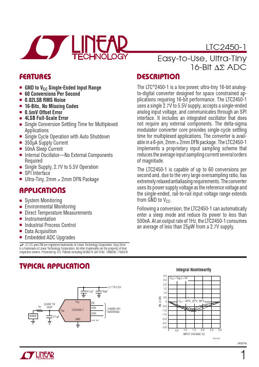
124501fbFEATURESAPPLICATIONSDESCRIPTION16-Bit ΔΣ ADCThe L TC ®2450-1 is a low power , ultra-tiny 16-bit analog-to-digital converter designed for space constrained ap-plications requiring 16-bit performance. The L TC2450-1 uses a single 2.7V to 5.5V supply, accepts a single-ended analog input voltage, and communicates through an SPI interface. It includes an integrated oscillator that does not require any external components. The delta-sigma modulator converter core provides single-cycle settling time for multiplexed applications. The converter is avail-able in a 6-pin, 2mm × 2mm DFN package. The L TC2450-1 implements a proprietary input sampling scheme that reduces the average input sampling current several orders of magnitude.The L TC2450-1 is capable of up to 60 conversions per second and, due to the very large oversampling ratio, has extremely relaxed antialiasing requirements. The converter uses its power supply voltage as the reference voltage and the single-ended, rail-to-rail input voltage range extends from GND to V CC .Following a conversion, the L TC2450-1 can automatically enter a sleep mode and reduce its power to less than 500nA. At an output rate of 1Hz, the L TC2450-1 consumes an average of less than 25μW from a 2.7V supply.nGND to V CC Single-Ended Input Range n 60 Conversions Per Second n 0.02LSB RMS Noisen 16-Bits, No Missing Codes n 0.5mV Offset Error n 4LSB Full-Scale ErrornSingle Conversion Settling Time for Multiplexed Applicationsn Single Cycle Operation with Auto Shutdown n 350μA Supply Current n 50nA Sleep Currentn Internal Oscillator—No External Components Requiredn Single Supply, 2.7V to 5.5V Operation n SPI Interface n Ultra-Tiny, 2mm × 2mm DFN PackagenSystem Monitoring n E nvironmental Monitoringn Direct Temperature Measurements n Instrumentationn Industrial Process Control n Data Acquisitionn Embedded ADC UpgradesIntegral NonlinearityL , L T , L TC and L TM are registered trademarks of Linear Technology Corporation. Easy Drive is a trademark of Linear Technology Corporation. All other trademarks are the property of their respective owners. Protected by U.S. Patents including 6208279, 6411242, 7088280, 7164378.INPUT VOL TAGE (V)–3.0I N L (L S B )–2.0–1.001.03.00.51.0 1.52.024501 G022.53.02.0–2.5–1.5–0.50.52.51.5V CC = V REF = 3VT A = –45°C, 25°C, 90°CT YPICAL APPLICATIONLTC2450-1224501fbPIN CONFIGURATIONABSOLUTE MAXIMUM RATINGSSupply Voltage (V CC ) ...................................–0.3V to 6V Analog Input Voltage (V IN ) ............–0.3V to (V CC + 0.3V)Digital Input Voltage ......................–0.3V to (V CC + 0.3V)Digital Output Voltage ...................–0.3V to (V CC + 0.3V)Operating Temperature RangeL TC2450C-1 .............................................0°C to 70°C L TC2450I-1 ..........................................–40°C to 85°C Storage Temperature Range ...................–65°C to 150°C(Notes 1, 2)PARAMETERCONDITIONSMIN TYP MAX UNITS Resolution (No missing codes)(Note 3)l 16Bits Integral Nonlinearity (Note 4)l 210LSB Offset Error l0.52mV Offset Error Drift 0.02LSB/°C Gain Error l0.010.02% of FS Gain Error Drift 0.02LSB/°C T ransition Noise1.4μV RMSThe l denotes the specifi cations which apply over the full operating temperature range, otherwise specifi cations are at T A = 25°C. (Note 2)SYMBOL PARAMETER CONDITIONSMIN TYP MAX UNITSV IN Input Voltage Range lV CCC ININ Sampling Capacitance 0.35pFI DC_LEAK (V IN )IN DC Leakage Current V IN = GND (Note 5)V IN = V CC (Note 5)l l–10–10111010nA nA I CONVInput Sampling Current (Note 9)50nAThe l denotes the specifi cations which apply over the full operating temperature range,otherwise specifi cations are at T A = 25°C.Lead Free FinishTAPE AND REEL (MINI)TAPE AND REELPART MARKING*PACKAGE DESCRIPTIONTEMPERATURE RANGE L TC2450CDC-1#TRMPBF L TC2450CDC-1#TRPBF LCTR 6-Lead (2mm × 2mm) Plastic DFN 0°C to 70°C L TC2450IDC-1#TRMPBF L TC2450IDC-1#TRPBF LCTR 6-Lead (2mm × 2mm) Plastic DFN –40°C to 85°CTRM = 500 pieces. *Temperature grades are identifi ed by a label on the shipping container .Consult L TC Marketing for parts specifi ed with wider operating temperature ranges.Consult L TC Marketing for information on lead based fi nish parts.For more information on lead free part marking, go to: http://www.linear .com/leadfree/For more information on tape and reel specifi cations, go to: http://www.linear .com/tapeandreel/TOP VIEWDC PACKAGE6-LEAD (2mm × 2mm) PLASTIC DFNV CC V IN GND 4576321SDO SCK CST JMAX = 125°C, θJA = 102°C/WEXPOSED PAD (PIN 17) IS GND, MUST BE SOLDERED TO PCBORDER INFORMATIONELECTRICAL CHARACTERISTICSANALOG INPUTLTC2450-1324501fbNote 1: Stresses beyond those listed under Absolute Maximum Ratings may cause permanent damage to the device. Exposure to any Absolute Maximum Rating condition for extended periods may affect device reliability and lifetime.Note 2: All voltage values are with respect to GND. V CC = 2.7V to 5.5V unless otherwise specifi ed.Note 3: Guaranteed by design, not subject to test.Note 4: Integral nonlinearity is defi ned as the deviation of a code from a straight line passing through the actual endpoints of the transfer curve. The deviation is measured from the center of the quantization band. Guaranteed by design, test correlation and 3 point transfer curve measurement.SYMBOL PARAMETER CONDITIONSMIN TYP MAX UNITSV CC Supply Voltage l 2.75.5V I CCSupply Current Conversion SleepCS = GND (Note 6)CS = V CC (Note 6)ll3500.056000.5μA μAThe l denotes the specifi cations which apply over the full operating temperature range,otherwise specifi cations are at T A = 25°C. (Note 2)POWER REQUIREMENTSSYMBOL PARAMETERCONDITIONSMINTYP MAX UNITSV IH High Level Input Voltage l V CC – 0.3V V IL Low Level Input Voltage l 0.3V I IN Digital Input Current l–1010μA C IN Digital Input Capacitance 10pF V OH High Level Output Voltage I O = –800μA l V CC – 0.5VV OL Low Level Output Voltage I O = –1.6mAl 0.4V I OZHi-Z Output Leakage Currentl–1010μAThe l denotes the specifi cations which apply over the full operating temperature range,otherwise specifi cations are at T A = 25°C.The l denotes the specifi cations which apply over the full operating temperature range,otherwise specifi cations are at T A = 25°C.SYMBOL PARAMETER CONDITIONSMIN TYP MAX UNITS t CONV Conversion Time l 1416.621ms f SCK SCK Frequency Range l 2MHz t lSCK SCK Low Period l 250ns t hSCK SCK High Periodl250nst 1CS Falling Edge to SDO Low Z (Notes 7, 8)l 0100ns t 2CS Rising Edge to SDO High Z(Notes 7, 8)l 0100ns t 3CS Falling Edge to SCK Falling Edge l 100ns t KQSCK Falling Edge to SDO Valid(Note 7)l100nsNote 5: CS = V CC . A positive current is fl owing into the DUT pin.Note 6: SCK = V CC or GND. SDO is high impedance.Note 7: See Figure 3.Note 8: See Figure 4.Note 9: Input sampling current is the average input current drawn from the input sampling network while the L TC2450-1 is actively sampling the input.DIGITAL INPUTS AND DIGITAL OUTPUTSTIMING CHARACTERISTICSLTC2450-1424501fbTYPICAL PERFORMANCE CHARACTERISTICSIntegral NonlinearityIntegral NonlinearityMaximum INL vs TemperatureOffset Error vs TemperatureGain Error vs TemperatureT ransition Noise vs TemperatureT ransition Noise vs Output CodeConversion Mode Power Supply Current vs TemperatureINPUT VOL TAGE (V)0–3.0I N L (L S B )–2.0–1.001.03.0 1.5 2.5 3.524501 G014.50.5 1.0 2.0 3.0 4.05.02.0–2.5–1.5–0.50.52.5 1.5V CC = V REF = 5VT A = –45°C, 25°C, 90°CINPUT VOL TAGE (V)–3.0I N L (L S B )–2.0–1.001.03.00.51.0 1.52.024501 G022.53.02.0–2.5–1.5–0.50.52.51.5V CC = V REF = 3VT A = –45°C, 25°C, 90°CTEMPERATURE (°C)–5076543210257524501 G04–2550100O F F S E T (L S B )TEMPERATURE (°C)–50–1G A I N E R R O R (L S B )1235–25025******* G05751004V CC = 4.1VV CC = 2.7VV CC = 5.5VTEMPERATURE (°C)–50 T R A N S I T I O N N O I S ER M S (μV )1.503.0010709024501 G061.000.250.500.752.502.001.252.7502.251.75–30–103050OUTPUT CODE (NORMALIZED TO FULL SCALE)0 T R A N S I T I O NN O I S E R M S (μV )1.503.000.80 1.0024501 G071.000.250.500.752.502.001.252.7502.251.750.200.400.60TEMPERATURE (°C)–45–250C O N V E R S I O N C U R R E N T (μA )200500–5355524501 G08100400300157595LTC2450-1524501fbSleep Mode Power Supply Current vs TemperatureTYPICAL PERFORMANCE CHARACTERISTICSConversion Period vs TemperatureAverage Supply Power vs Temperature, V CC = 3VTEMPERATURE (°C)–45–250S L E E P M O D E C U R R E N T (n A )100250–5355524501 G0950200150157595TEMPERATURE (°C)–45192022155524501 G111817–25–5357595161521C O N V E R S I O N T I M E(m s )TEMPERATURE (°C)–5010A V E R A G E S U P P L Y P O W E R (μW )100100010000–250255024501 G1075100LTC2450-1624501fbPIN FUNCTIONSV CC (Pin 1): Positive Supply Voltage and Converter Refer-ence Voltage. Bypass to GND (Pin 3) with a 10μF capacitor in parallel with a low series inductance 0.1μF capacitor located as close to the part as possible.V IN (Pin 2): Analog Input Voltage.GND (Pin 3): Ground. Connect to a ground plane through a low impedance connection.CS (Pin 4): Chip Select (Active LOW) Digital Input. A LOW on this pin enables the SDO digital output. A HIGH on this pin places the SDO output pin in a high imped-ance state.SDO (Pin 5): Three-State Serial Data Output. SDO is used for serial data output during the DATA OUTPUT state and can be used to monitor the conversion status.SCK (Pin 6): Serial Clock Input. SCK synchronizes the serial data output. While digital data is available (the ADC is not in CONVERT state) and CS is LOW (ADC is not in SLEEP state) a new data bit is produced at the SDO output pin following every falling edge applied to the SCK pin.Exposed Pad (Pin 7): Ground. The Exposed Pad must be soldered to the same point as Pin 3.Figure 1. Functional Block DiagramV V 24501 BDFUNCTIONAL BLOCK DIAGRAMLTC2450-1724501fbCONVERTER OPERATIONConverter Operation Cycle The L TC2450-1 is a low power , delta-sigma analog-to-digital converter with a simple 3-wire interface (see Figure 1). Its operation is composed of three successive states: CONVERT , SLEEP and DATA OUTPUT . The operat-ing cycle begins with the CONVE RT state, is followed by the SLE E P state, and ends with the DATA OUTPUT state (see Figure 2). The 3-wire interface consists of serial data output (SDO), serial clock input (SCK), and the active low chip select input (CS ). The CONVE RT state duration is determined by the L TC2450-1 conversion time (nominally 16.6 milliseconds). Once started, this operation can not be aborted except by a low power supply condition (V CC < 2.1V) which generates an internal power-on reset signal.After the completion of a conversion, the L TC2450-1enters the SLEEP state and remains there until both the chip select and clock inputs are low (CS = SCK = LOW). Following this condition the ADC transitions into the DATA OUTPUT state.Figure 2. L TC2450-1 State T ransition DiagramAPPLICATIONS INFORMATIONWhile in the SLEEP state, whenever the chip select in-put is pulled high (CS = HIGH), the L TC2450-1’s powersupply current is reduced to less than 500nA. When the chip select input is pulled low (CS = LOW), and SCK is maintained at a HIGH logic level, the L TC2450-1 will return to a normal power consumption level. During the SLEEPstate, the result of the last conversion is held indefinitely in a static register .Upon entering the DATA OUTPUT state, SDO outputs the most signifi cant bit (D15) of the conversion result. During this state, the ADC shifts the conversion result serially through the SDO output pin under the control of the SCK input pin. There is no latency in generating this data and the result corresponds to the last completed conversion. A new bit of data appears at the SDO pin following each falling edge detected at the SCK input pin. The user canreliably latch this data on every rising edge of the external serial clock signal driving the SCK pin (see Figure 3).The DATA OUTPUT state concludes in one of two different ways. First, the DATA OUTPUT state operation is completed once all 16 data bits have been shifted out and the clockthen goes low. This corresponds to the 16th falling edge of SCK. Second, the DATA OUTPUT state can be abortedat any time by a LOW-to-HIGH transition on the CS input. Following either one of these two actions, the L TC2450-1will enter the CONVERT state and initiate a new conver-sion cycle.Power-Up SequenceWhen the power supply voltage V CC applied to the con-verter is below approximately 2.1V , the ADC performs apower-on reset. This feature guarantees the integrity of the conversion result.When V CC rises above this critical threshold, the converter generates an internal power-on reset (POR) signal for approximately 0.5ms. The POR signal clears all internal registers. Following the POR signal, the L TC2450-1 starts a conversion cycle and follows the succession of states described in Figure 2. The fi rst conversion result fol-lowing POR is accurate within the specifi cations of the device if the power supply voltage V CC is restored within the operating range (2.7V to 5.5V) before the end of the POR time interval.LTC2450-1824501fbAPPLICATIONS INFORMATIONInput Voltage RangeThe ADC is capable of digitizing true rail-to-rail input sig-nals. Ignoring offset and full-scale errors, the converter will theoretically output an “all zero” digital result when the input is at ground (a zero scale input) and an “all one” digital result when the input is at V CC (a full-scale input). In an under-range condition, for all input voltages less than the voltage corresponding to output code 0, the converter will generate the output code 0. In an over-range condition, for all input voltages greater than the voltage corresponding to output code 65535 the converter will generate the output code 65535.Output Data FormatThe L TC2450-1 generates a 16-bit direct binary encoded result. It is provided, MSB fi rst, as a 16-bit serial stream through the SDO output pin under the control of the SCK input pin (see Figure 3).During the data output operation the CS input pin must be pulled low (CS = LOW). The data output process starts with the most signifi cant bit of the result being present at the SDO output pin (SDO = D15) once CS goes low. A new data bit appears at the SDO output pin following every falling edge detected at the SCK input pin. The output data can be reliably latched by the user using the rising edge of SCK.Ease of UseThe L TC2450-1 data output has no latency, fi lter settling delay or redundant results associated with the conversion cycle. There is a one-to-one correspondence between the conversion and the output data. Therefore, multiplexing multiple analog input voltages requires no special ac-tions.The L TC2450-1 includes a proprietary input sampling scheme that reduces the average input current several orders of magnitude as compared to traditional delta sigma architectures. This allows external fi lter networks to interface directly to the L TC2450-1. Since the average input sampling current is 50nA, an external RC lowpass fi lter using a 1k Ω and 0.1μF results in <1LSB error .Reference Voltage RangeThe converter uses the power supply voltage (V CC ) as the positive reference voltage (see Figure 1). Thus, the refer-ence range is the same as the power supply range, which extends from 2.7V to 5.5V . The L TC2450-1’s internal noise level is extremely low so the output peak-to-peak noise remains well below 1LSB for any reference voltage within this range. Thus the converter resolution remains at 1LSB independent of the reference voltage. INL, offset, and full-scale errors vary with the reference voltage as indicated by the Typical Performance Characteristics graphs. These error terms will decrease with an increase in the reference voltage (as the LSB size in μV increases).Figure 3. Data Output TimingKQlSCKhSCKLTC2450-1924501fbConversion Status MonitorFor certain applications, the user may wish to monitor the L TC2450-1 conversion status. This can be achieved by holding SCK HIGH during the conversion cycle. In this condition, whenever the CS input pin is pulled low (CS = LOW), the SDO output pin will provide an indication of the conversion status. SDO = HIGH is an indication of a conversion cycle in progress while SDO = LOW is an indication of a completed conversion cycle. An example of such a sequence is shown in Figure 4.Conversion s tatus m onitoring, w hile p ossible, i s n ot r equired for L TC2450-1 as its conversion time is fi xed and equal at approximately 16.6ms (21ms maximum). Therefore, ex-ternal timing can be used to determine the completion of a conversion cycle. SERIAL INTERFACEThe L TC2450-1 transmits the conversion result and receives the start of conversion command through a synchronous 3-wire interface. This interface can be used during the CONVE RT and SLE E P states to assess the conversion status and during the DATA OUTPUT state to read the conversion result, and to trigger a new conversion.APPLICATIONS INFORMATIONSerial Interface Operation ModesThe following are a few of the more common interface operation examples. Many more valid control and serial data output operation sequences can be constructed based upon the above description of the function of the three digital interface pins.The modes of operation can be summarized as follows:1) The L TC2450-1 functions with SCK idle high (commonly known as CPOL = 1) or idle low (commonly known as CPOL = 0).2) After the 16th bit is read, the user can choose one of two ways to begin a new conversion. First, one can pull CS high (CS = ↑). Second, one can use a high-low transition on SCK (SCK = ↓).3) At any time during the Data Output state, pulling CS high (CS = ↑) causes the part to leave the I/O state, abort the output and begin a new conversion.4) When SCK = HIGH, it is possible to monitor the conver-sion status by pulling CS low and watching for SDO to go low. This feature is available only in the idle-high (CPOL = 1) mode.Figure 4. Conversion Status Monitoring ModeSDOSCK = HICSLTC2450-11024501fbAPPLICATIONS INFORMATIONSerial Clock Idle-High (CPOL = 1) ExamplesIn Figure 5, following a conversion cycle the L TC2450-1 automatically enters the low power sleep mode. The user can monitor the conversion status at convenient intervals using CS and SDO.CS is pulled LOW while SCK is HIGH to test whether or not the chip is in the CONVERT state. While in the CONVERT state, SDO is HIGH while CS is LOW . In the SLEEP state, SDO is LOW while CS is LOW . These tests are not required operational steps but may be useful for some applications.When the data is available, the user applies 16 clock cycles to transfer the result. The CS rising edge is then used to initiate a new conversion.The operation example of Figure 6 is identical to that of Figure 5, except the new conversion cycle is triggered bythe falling edge of the serial clock (SCK). A 17th clock pulse is used to trigger a new conversion cycle.Serial Clock Idle-Low (CPOL = 0) ExamplesIn Figure 7, following a conversion cycle the L TC2450-1 automatically enters the low power sleep state. The user determines data availability (and the end of conversion) based upon external timing. The user then pulls CS low (CS = ↓) and uses 16 clock cycles to transfer the result. Following the 16th rising edge of the clock, CS is pulled high (CS = ↑), which triggers a new conversion.The timing diagram in Figure 8 is identical to that of Figure 7, except in this case a new conversion is triggered by SCK. The 16th SCK falling edge triggers a new conversion cycle and the CS signal is subsequently pulled high.Figure 5. Idle-High (CPOL = 1) Serial Clock Operation Example.The Rising Edge of CS Starts a New ConversionFigure 6. Idle-High (CPOL = 1) Clock Operation Example.A 17th Clock Pulse is Used to Trigger a New Conversion CycleLTC2450-11124501fbExamples of Aborting Cycle using CSFor some applications the user may wish to abort the I/O cycle and begin a new conversion. If the L TC2450-1 is in the data output state, a CS rising edge clears the remaining data bits from memory, aborts the output cycle and triggers a new conversion. Figure 9 shows an example of aborting an I/O with idle-high (CPOL = 1) and Figure 10 shows an example of aborting an I/O with idle-low (CPOL = 0).A new conversion cycle can be triggered using the CS signal without having to generate any serial clock pulses as shown in Figure 11. If SCK is maintained at a LOW logic level, after the end of a conversion cycle, a newconversion operation can be triggered by pulling CS low and then high. When CS is pulled low (CS = LOW), SDO will output the most signifi cant bit (D15) of the result of the just completed conversion. While a low logic level is maintained at SCK pin and CS is subsequently pulled high (CS = HIGH) the remaining 15 bits of the result (D14:D0) are discarded and a new conversion cycle starts.Following the aborted I/O, additional clock pulses in the CONVERT state are acceptable, but excessive signal tran-sitions on SCK can potentially create noise on the ADC during the conversion, and thus may negatively infl uence the conversion accuracy.APPLICATIONS INFORMATIONFigure 8. Idle-Low (CPOL = 0) Clock. The 16th SCK Falling Edge T riggers a New ConversionFigure 7. Idle-Low (CPOL = 0) Clock. C S T riggers a New ConversionLTC2450-1APPLICATIONS INFORMATIONFigure 9. Idle-High (CPOL = 1) Clock and Aborted I/O ExampleFigure 10. Idle-Low (CPOL = 0) Clock and Aborted I/O ExampleFigure 11. Idle-Low (CPOL = 0) Clock and Minimum Data Output Length Example 1224501fbLTC2450-11324501fbAPPLICATIONS INFORMATIONFigure 12. 2-Wire, Idle-High (CPOL = 1) Serial Clock, Operation ExampleFigure 13. 2-Wire, Idle-Low (CPOL = 0) Serial Clock Operation Example2-Wire OperationThe 2-wire operation modes, while reducing the number of required control signals, should be used only if the L TC2450-1 low power sleep capability is not required. In addition the option to abort serial data transfers is no longer available. Hardwire CS to GND for 2-wire operation.Figure 12 shows a 2-wire operation sequence which uses an idle-high (CPOL = 1) serial clock signal. The conversion status can be monitored at the SDO output. Following a conversion cycle, the ADC enters SLEEP state and the SDO output transitions from HIGH to LOW . Subsequently 16 clock pulses are applied to the SCK input in order to serially shift the 16 bit result. Finally, the 17th clock pulse is applied to the SCK input in order to trigger a new conversion cycle.Figure 13 shows a 2-wire operation sequence which uses an idle-low (CPOL = 0) serial clock signal. The conversionstatus cannot be monitored at the SDO output. Following a conversion cycle, the L TC2450-1 bypasses the SLEEP state and immediately enters the DATA OUTPUT state. At this moment the SDO pin outputs the most signifi cant bit (D15) of the conversion result. The user must use external timing in order to determine the end of conversion and result availability. Subsequently 16 clock pulses are applied to SCK in order to serially shift the 16-bit result. The 16th clock falling edge triggers a new conversion cycle.PRESERVING THE CONVERTER ACCURACYThe L TC2450-1 is designed to reduce as much as possible the conversion result sensitivity to device decoupling, PCB layout, antialiasing circuits, line and frequency perturbations. Nevertheless, in order to preserve the very high accuracy capability of this part, some simple precautions are desirable.LTC2450-11424501fbAPPLICATIONS INFORMATIONDigital Signal LevelsThe L TC2450-1’s digital interface is easy to use. Its digital inputs (SCK and CS ) accept standard CMOS logic levels and the internal hysteresis receivers can tolerate edge rates as slow as 100μs. However , some considerations are required to take advantage of the exceptional accuracy and low supply current of this converter .The digital output signal SDO is less of a concern because it is not active during the conversion cycle.While a digital input signal is in the range 0.5V to V CC –0.5V , the CMOS input receiver may draw additional current from the power supply. Due to the nature of CMOS logic, a slow transition within this voltage range may cause an increase in the power supply current drawn by the converter , particularly in the low power operation mode within the SLEEP state. Thus, for low power consumption it is highly desirable to provide relatively fast edges for the two digital input pins SCK and CS , and to keep the digital input logic levels at V CC or GND.At the same time, during the CONVERT state, undershoot and/or overshoot of fast digital signals connected to the L TC2450-1 pins may affect the conversion result. Under-shoot and overshoot can occur because of an impedance mismatch at the converter pin combined with very fast transition times. This problem becomes particularly diffi cult when shared control lines are used and multiple refl ec-tions may occur . The solution is to carefully terminate all transmission lines close to their characteristic impedance. Parallel termination is seldom an acceptable option in low power systems so a series resistor between 27Ω and 56Ω placed near the driver may eliminate this problem. The actual resistor value depends upon the trace impedance and connection topology. An alternate solution is to reduce the edge rate of the control signals, keeping in mind the concerns regarding slow edges mentioned above.Particular attention should be given to confi gurations in which a continuous clock signal is applied to SCK pin dur-ing the CONVERT state. While L TC2450-1 will ignore this signal from a logic point of view the signal edges may create unexpected errors depending upon the relation between its frequency and the internal oscillator frequency. In such a situation it is benefi cial to use edge rates of about 10nsand to limit potential undershoot to less than 0.3V belowGND and overshoot to less than 0.3V above V CC .Noisy external circuitry can potentially impact the output under 2-wire operation. In particular , it is possible to get the L TC2450-1 into an unknown state if an SCK pulse is missed or noise triggers an extra SCK pulse. In this situ-ation, it is impossible to distinguish SDO = 1 (indicating conversion in progress) from valid “1” data bits. As such, CPOL = 1 is recommended for the 2-wire mode. The user should look for SDO = 0 before reading data, and look for SDO = 1 after reading data. If SDO does not return a “0” within the maximum conversion time (or return a “1” after a full data read), generate 16 SCK pulses to force a new conversion.Driving V CC and GNDThe V CC and GND pins of the L TC2450-1 converter are directly connected to the positive and negative reference voltages, respectively. A simplifi ed equivalent circuit is shown in Figure 14.The power supply current passing through the parasitic layout resistance associated with these common pins will modify the ADC reference voltage and thus negatively affect the converter accuracy. It is thus important to keep the V CC and GND lines quiet, and to connect these supplies through very low impedance traces.In relation to the V CC and GND pins, the L TC2450-1 com-bines internal high frequency decoupling with dampingFigure 14. L TC2450-1 Analog Pins Equivalent CircuitR SW (TYP)C EQ (TYP)0.35pFINTERNAL SWITCHING FREQUENCY = 4 MHz。

基于LTC4020的多功能充电器的研究与设计①董巧攀(新乡市太行电源设备有限公司,河南新乡 453000)摘要:本文是以LTC4020控制器为核心研究设计的多功能充电器,LTC4020采用高转换效率的同步降压-升压电源变换结构,输入电压高于或低于输出电压均可工作;内置多种电池充电模式可满足常规各种电池的充电需求;而且具有适合太阳能电池板充电的最大功功率点跟踪功能MPPT。
本文研究的多功能充电器适应多种输入电源类型,以及为多种类型电池充电,特别是在野外作战、紧急救援等特殊情况下可以满足多种装备的充电需求。
关键词:多功能充电器;LTC4020;降压-升压电源变换;MPPT中图分类号:TM 911.4 文献标识码:A 文章编号:1008-7923(2020)03-0126-04Research and Design of Multifunctional Charger Based on LTC4020DONG Qiao-pan(Xinxiang Taihang Power Source Equipment Co.,Ltd.,Xinxiang,Henan Province,453000,China.)Abstract:The text is a multifunctional charger designed with LTC4020controller as the coreresearch and design.LTC4020adopts a high conversion efficiency synchronous buck-boost powerconversion structure,which can work with input voltage higher or lower than output voltage;built-in multiple battery charging the mode can meet the charging requirements of various con-ventional batteries;and has the maximum power point tracking function MPPT suitable for solarpanel charging.The multi-function charger studied in this paper is suitable for a variety of inputpower types,as well as for charging a variety of types of batteries,especially in special situationssuch as field operations and emergency rescue,which can meet the charging needs of a variety ofequipment.Keywords:Multifunctional Charger;LTC4020;Buck-boost power conversion;MPPT1 引言随着科技进步电子产品迅速发展,无论是野外救援、户外勘探、军用通信等领域的电子设备或无人值守设备都离不开蓄电池组。
12LTC24403sn2440, 2440fasSYMBOL PARAMETERCONDITIONSMIN TYP MAX UNITSIN +Absolute/Common Mode IN + Voltage ●GND – 0.3V V CC + 0.3V V IN –Absolute/Common Mode IN – Voltage ●GND – 0.3V V CC + 0.3V V V IN Input Differential Voltage Range ●–V REF /2V REF /2V (IN + – IN –)REF +Absolute/Common Mode REF + Voltage ●0.1V CC V REF –Absolute/Common Mode REF – Voltage ●GND V CC – 0.1V V V REF Reference Differential Voltage Range ●0.1V CCV (REF + – REF –)C S(IN+)IN + Sampling Capacitance 3.5pF C S(IN–)IN – Sampling Capacitance 3.5pF C S(REF+)REF + Sampling Capacitance 3.5pF C S(REF–)REF – Sampling Capacitance3.5pFI DC_LEAK(IN+, IN–,Leakage Current, Inputs and Reference CS = V CC , IN + = GND, IN – = GND,●–10010100nAREF+, REF–)REF + = 5V, REF – = GNDI SAMPLE(IN+, IN–,Average Input/Reference Current Varies, See Applications SectionREF+, REF–)During SamplingThe ● denotes specifications which apply over the full operatingtemperature range, otherwise specifications are at T A = 25°C. (Note 3)A ALOG I PUT A U D REFERE CE U UUThe ● denotes specifications which apply over the fulloperating temperature range, otherwise specifications are at T A = 25°C. (Note 3)SYMBOL PARAMETERCONDITIONS MINTYP MAX UNITSV IH High Level Input Voltage 4.5V ≤ V CC ≤ 5.5V ● 2.5VCS, F OV IL Low Level Input Voltage 4.5V ≤ V CC ≤ 5.5V●0.8V CS, F OV IH High Level Input Voltage 4.5V ≤ V CC ≤ 5.5V (Note 8)● 2.5V SCKV IL Low Level Input Voltage 4.5V ≤ V CC ≤ 5.5V (Note 8)●0.8V SCKI IN Digital Input Current 0V ≤ V IN ≤ V CC●–1010µA CS, F OI IN Digital Input Current 0V ≤ V IN ≤ V CC (Note 8)●–1010µA SCKC IN Digital Input Capacitance 10pF CS, F OC IN Digital Input Capacitance (Note 8)10pF SCKV OH High Level Output Voltage I O = –800µA ●V CC – 0.5VVSDO, BUSYV OL Low Level Output Voltage I O = 1.6mA ●0.4VV SDO, BUSYV OH High Level Output Voltage I O = –800µA (Note 9)●V CC – 0.5VV SCKV OL Low Level Output Voltage I O = 1.6mA (Note 9)●0.4VV SCKI OZHi-Z Output Leakage ●–1010µASDODIGITAL I PUTS A D DIGITAL OUTPUTSU ULTC24404sn2440, 2440fasSYMBOL PARAMETER CONDITIONSMIN TYP MAX UNITSV CC Supply Voltage ● 4.55.5V I CCSupply CurrentConversion Mode CS = 0V (Note 7)●811mA Sleep ModeCS = V CC (Note 7)●830µAThe ● denotes specifications which apply over the full operating temperature range,otherwise specifications are at T A = 25°C. (Note 3)POWER REQUIRE E T SWU SYMBOL PARAMETERCONDITIONSMIN TYP MAX UNITS f EOSC External Oscillator Frequency Range ●0.120MHz t HEO External Oscillator High Period ●2510000ns t LEO External Oscillator Low Period ●2510000ns t CONVConversion TimeOSR = 256 (SDI = 0)●0.99 1.13 1.33ms OSR = 32768 (SDI = 1)●126145170ms External Oscillator (Note 10, 13)●40 • OSR + 170f EOSC (kHz)msf ISCK Internal SCK Frequency Internal Oscillator (Note 9)●0.80.91MHz External Oscillator (Notes 9, 10)f EOSC /10Hz D ISCK Internal SCK Duty Cycle (Note 9)●4555%f ESCK External SCK Frequency Range (Note 8)●20MHz t LESCK External SCK Low Period (Note 8)●25ns t HESCK External SCK High Period(Note 8)●25ns t DOUT_ISCK Internal SCK 32-Bit Data Output Time Internal Oscillator (Notes 9, 11)●41.635.330.9µs External Oscillator (Notes 9, 10)●320/f EOSC s t DOUT_ESCK External SCK 32-Bit Data Output Time (Note 8)●32/f ESCKs t 1CS ↓ to SDO Low Z (Note 12)●025ns t 2CS ↑ to SDO High Z (Note 12)●025ns t 3CS ↓ to SCK ↓(Note 9)5µs t 4CS ↓ to SCK ↑(Notes 8, 12)●25ns t KQMAX SCK ↓ to SDO Valid ●25ns t KQMIN SDO Hold After SCK ↓(Note 5)●15ns t 5SCK Set-Up Before CS ↓●50ns t 7SDI Setup Before SCK ↑●10Note 5ns t 8SDI Hold After SCK ↑●10Note 5nsThe ● denotes specifications which apply over the full operating temperaturerange, otherwise specifications are at T A = 25°C. (Note 3)TI I G CHARACTERISTICSWU Note 1: Absolute Maximum Ratings are those values beyond which the life of the device may be impaired.Note 2: All voltage values are with respect to GND.Note 3: V CC = 4.5 to 5.5V unless otherwise specified.V REF = REF + – REF –, V REFCM = (REF + + REF –)/2;V IN = IN + – IN –, V INCM = (IN + + IN –)/2.Note 4: F O pin tied to GND or to external conversion clock source with f EOSC = 10MHz unless otherwise specified.Note 5: Guaranteed by design, not subject to test.Note 6: Integral nonlinearity is defined as the deviation of a code from a straight line passing through the actual endpoints of the transfer curve.The deviation is measured from the center of the quantization band.Note 7: The converter uses the internal oscillator.Note 8: The converter is in external SCK mode of operation such that the SCK pin is used as a digital input. The frequency of the clock signal driving SCK during the data output is f ESCK and is expressed in Hz.Note 9: The converter is in internal SCK mode of operation such that the SCK pin is used as a digital output. In this mode of operation, the SCK pin has a total equivalent load capacitance of C LOAD = 20pF.Note 10: The external oscillator is connected to the F O pin. The external oscillator frequency, f EOSC , is expressed in kHz.Note 11: The converter uses the internal oscillator. F O = 0V.Note 12: Guaranteed by design and test correlation.Note 13: There is an internal reset that adds an additional 1µs (typical) to the conversion time.5sn2440, 2440fasV IN (V)–2.5 1.52440 G01–1.5–0.50 2.50.5–2–121V IN (V)–2.5 1.52440 G02–1.5–0.50 2.50.5–2–121V IN (V)–2.5 1.52440 G03–1.5–0.50 2.50.5–2–121V CC = 5V V REF = 5V V REF + = 5VV REF –= GNDV INCM = 2.5V F O = GND T A = 25°CV CC = 5V V REF = 5V V REF + = 5VV REF –= GNDV INCM = 2.5V F O = GND T A = 25°CV IN (V)–2.5 1.52440 G06–1.5–0.50 2.50.5–2–121V CC = 5V V REF = 5V V REF + = 5VV REF –= GNDV INCM = 2.5V F O = GND T A = 25°CV IN (V)–2.5 1.52440 G07–1.5–0.50 2.50.5–2–121V CC = 5V V REF = 5V V REF + = 5VV REF –= GNDV INCM = 2.5V F O = GND T A = 25°CV IN (V)–2.5 1.52440 G08 –1.5–0.50 2.50.5–2–121V CC = 5V V REF = 5V V REF + = 5VV REF –= GNDV INCM = 2.5V F O = GND T A = 25°CV IN (V)–2.5 1.52440 G09–1.5–0.50 2.50.5–2–121V CC = 5V V REF = 5V V REF + = 5VV REF –= GNDV INCM = 2.5V F O = GND T A = 25°CIntegral Nonlinearity f OUT = 440HzIntegral Nonlinearity f OUT = 220HzIntegral Nonlinearity f OUT = 110HzIntegral Nonlinearity f OUT = 55HzIntegral Nonlinearity f OUT = 27.5HzIntegral Nonlinearity f OUT = 13.75Hz6V IN (V)–2.5 1.52440 G10–1.5–0.50 2.50.5–2–121V IN (V)–1.250.752440 G12–0.75–0.25 1.250.25V CC = 5V V REF = 2.5VV REF + = 2.5V V REF – = GND OSR = 32768F O = GND T A = 25°C V INCM = 1.25VV INCM = 3.75VV INCM = 2.5VIntegral Nonlinearity vs TemperatureV IN (V)2440 G13V CC = 5V V REF = 2.5V V REF + = 2.5VV REF –= GNDV INCM = 1.25V OSR = 32768F O = GND2440 G14–Full-Scale Error vs V REF+Full-Scale Error vs V REF–Full-Scale Error vs V CCRMS Noise vs Output Rate(OSR = 128) External Clock Sweep 10MHz to 20MHz7LTC24408sn2440, 2440fasGND (Pins 1, 8, 9, 16): Ground. Multiple ground pins internally connected for optimum ground current flow and V CC decoupling. Connect each one of these pins to a ground plane through a low impedance connection. All four pins must be connected to ground for proper operation.V CC (Pin 2): Positive Supply Voltage. Bypass to GND (Pin 1) with a 10µF tantalum capacitor in parallel with 0.1µF ceramic capacitor as close to the part as possible.REF + (Pin 3), REF – (Pin 4): Differential Reference Input.The voltage on these pins can have any value between GND and V CC as long as the reference positive input, REF +, is maintained more positive than the reference negative input, REF –, by at least 0.1V.IN + (Pin 5), IN – (Pin 6): Differential Analog Input. The voltage on these pins can have any value between GND – 0.3V and V CC + 0.3V. Within these limits the con-verter bipolar input range (V IN = IN + – IN –) extends from –0.5 • (V REF ) to 0.5 • (V REF ). Outside this input range the converter produces unique overrange and underrange output codes.SDI (Pin 7): Serial Data Input. This pin is used to select the speed/resolution of the converter. If SDI is grounded (pin compatible with LTC2410) the device outputs data at 880Hz with 21 bits effective resolution. By tying SD I HIGH, the converter enters the ultralow noise mode (200nV RMS ) with simultaneous 50/60Hz rejection at 6.9Hz output rate. SD I may be driven logic HIGH or LOW anytime during the conversion or sleep state in order to change the speed/resolution. The conversion immedi-ately following the data output cycle will be valid and performed at the newly selected output rate/resolution.SD I may also be programmed by a serial input data stream under control of SCK during the data output cycle.One of ten speed/resolution ranges (from 6.9Hz/200nV RMS to 3.5kHz/21µV RMS ) may be selected. The first conver-sion following a new selection is valid and performed at the newly selected speed/resolution.EXT (Pin 10): Internal/External SCK Selection Pin. This pin is used to select internal or external SCK for outputting data. If EXT is tied low (pin compatible with the LTC2410),the device is in the external SCK mode and data is shifted out the device under the control of a user applied serial clock. If EXT is tied high, the internal serial clock mode isselected. The device generates its own SCK signal and outputs this on the SCK pin. A framing signal BUSY (Pin 15) goes low indicating data is being output.CS (Pin 11): Active LOW Digital Input. A LOW on this pin enables the SDO digital output and wakes up the ADC.Following each conversion the ADC automatically enters the Sleep mode and remains in this low power state as long as CS is HIGH. A LOW-to-HIGH transition on CS during the Data Output transfer aborts the data transfer and starts a new conversion.SDO (Pin 12): Three-State Digital Output. During the Data Output period, this pin is used as serial data output. When the chip select CS is HIGH (CS = V CC ) the SDO pin is in a high impedance state. During the Conversion and Sleep periods, this pin is used as the conversion status output.The conversion status can be observed by pulling CS LOW.SCK (Pin 13): Bidirectional Digital Clock Pin. In Internal Serial Clock Operation mode, SCK is used as digital output for the internal serial interface clock during the D ata Output period. In External Serial Clock Operation mode,SCK is used as digital input for the external serial interface clock during the D ata Output period. The Serial Clock Operation mode is determined by the logic level applied to the EXT pin.F O (Pin 14): Frequency Control Pin. Digital input that con-trols the internal conversion clock. When F O is connected to V CC or GND, the converter uses its internal oscillator running at 9MHz. The conversion rate is determined by the selected OSR such that t CONV (in ms) = (40 • OSR + 170)/9000 (t CONV = 1.137ms at OSR = 256, t CONV = 146ms at OSR = 32768). The first null is located at 8/t CONV , 7kHz at OSR = 256 and 55Hz (simultaneous 50/60Hz) at OSR = 32768.When F O is driven by an oscillator with frequency f EOSC (in kHz), the conversion time becomes t CONV = (40 • OSR +170)/f EOSC (in ms) and the first null remains 8/t CONV .BUSY (Pin 15): Conversion in Progress Indicator. For compatibility with the LTC2410, this pin should not be tied to ground. This pin is HIGH while the conversion is in progress and goes LOW indicating the conversion is complete and data is ready. It remains low during the sleep and data output states. At the conclusion of the data output state, it goes HIGH indicating a new conversion has begun.PI FU CTIO SU U U9LTC244010sn2440, 2440fasoperation cycle and data out format is compatible with the LTC2410.Initially, the LTC2440 performs a conversion. Once the conversion is complete, the device enters the sleep state.While in this sleep state, power consumption is reduced below 10µA. The part remains in the sleep state as long as CS is HIGH. The conversion result is held indefinitely in a static shift register while the converter is in the sleep state.Once CS is pulled LOW, the device begins outputting the conversion result. There is no latency in the conversion result. The data output corresponds to the conversion just performed. This result is shifted out on the serial data out pin (SDO) under the control of the serial clock (SCK). Data is updated on the falling edge of SCK allowing the user to reliably latch data on the rising edge of SCK (see Figure 3).The data output state is concluded once 32-bits are read out of the ADC or when CS is brought HIGH. The device au-tomatically initiates a new conversion and the cycle repeats.Through timing control of the CS, SCK and EXT pins, the LTC2440 offers several flexible modes of operation (internal or external SCK). These various modes do not require programming configuration registers; moreover,they do not disturb the cyclic operation described above.These modes of operation are described in detail in the Serial Interface Timing Modes section.Ease of UseThe LTC2440 data output has no latency, filter settling delay or redundant data associated with the conversion cycle. There is a one-to-one correspondence between the conversion and the output data. Therefore, multiplexing multiple analog voltages is easy. Speed/resolution ad-justments may be made seamlessly between two conver-sions without settling errors.The LTC2440 performs offset and full-scale calibrations every conversion cycle. This calibration is transparent to the user and has no effect on the cyclic operation de-scribed above. The advantage of continuous calibration is extreme stability of offset and full-scale readings with re-spect to time, supply voltage change and temperature drift.APPLICATIO S I FOR ATIOW UUU Power-Up SequenceThe LTC2440 automatically enters an internal reset state when the power supply voltage V CC drops below approximately 2.2V. This feature guarantees the integrity of the conversion result and of the serial interface mode selection.When the V CC voltage rises above this critical threshold,the converter creates an internal power-on-reset (POR)signal with a duration of approximately 0.5ms. The POR signal clears all internal registers. Following the POR signal, the LTC2440 starts a normal conversion cycle and follows the succession of states described above. The first conversion result following POR is accurate within the specifications of the device if the power supply voltage is restored within the operating range (4.5V to 5.5V) before the end of the POR time interval.Reference Voltage RangeThis converter accepts a truly differential external refer-ence voltage. The absolute/common mode voltage speci-fication for the REF + and REF – pins covers the entire range from GND to V CC . For correct converter operation, the REF + pin must always be more positive than the REF – pin.The LTC2440 can accept a differential reference voltage from 0.1V to V CC . The converter output noise is deter-mined by the thermal noise of the front-end circuits, and as such, its value in microvolts is nearly constant with reference voltage. A decrease in reference voltage will not significantly improve the converter’s effective resolution.On the other hand, a reduced reference voltage will im-prove the converter’s overall INL performance.Input Voltage RangeThe analog input is truly differential with an absolute/common mode range for the IN + and IN – input pins extending from GND – 0.3V to V CC + 0.3V. Outside these limits, the ESD protection devices begin to turn on and the errors due to input leakage current increase rapidly. Within these limits, the LTC2440 converts the bipolar differential input signal, V IN = IN + – IN –, from –FS = –0.5 • V REF to +FS = 0.5 • V REF where V REF =11LTC244012sn2440, 2440fassignal may be used as an interrupt for an externalmicrocontroller. Bit 31 (EOC) can be captured on the first rising edge of SCK. Bit 30 is shifted out of the device on the first falling edge of SCK. The final data bit (Bit 0) is shifted out on the falling edge of the 31st SCK and may be latched on the rising edge of the 32nd SCK pulse. On the falling edge of the 32nd SCK pulse, SDO goes HIGH indicating the initiation of a new conversion cycle. This bit serves as EOC (Bit 31) for the next conversion cycle. Table 2 summarizes the output data format.As long as the voltage on the IN + and IN – pins is maintained within the –0.3V to (V CC + 0.3V) absolute maximum operating range, a conversion result is generated for any differential input voltage V IN from –FS = –0.5 • V REF to +FS = 0.5 • V REF . For differential input voltages greater than +FS, the conversion result is clamped to the value corre-sponding to the +FS + 1LSB. For differential input voltages below –FS, the conversion result is clamped to the value corresponding to –FS – 1LSB.SERIAL INTERFACE PINSThe LTC2440 transmits the conversion results and re-ceives the start of conversion command through a synchronous 2-wire, 3-wire or 4-wire interface. During the conversion and sleep states, this interface can be used to assess the converter status and during the data output state it is used to read the conversion result and program the speed/resolution.Serial Clock Input/Output (SCK)The serial clock signal present on SCK (Pin 13) is used to synchronize the data transfer. Each bit of data is shifted out the SDO pin on the falling edge of the serial clock.In the Internal SCK mode of operation, the SCK pin is an output and the LTC2440 creates its own serial clock. In the External SCK mode of operation, the SCK pin is used as input. The internal or external SCK mode is selected by tying EXT (Pin 10) LOW for external SCK and HIGH for internal SCK.Serial Data Output (SDO)The serial data output pin, SDO (Pin 12), provides the result of the last conversion as a serial bit stream (MSB first) during the data output state. In addition, the SDO pin is used as an end of conversion indicator during the conversion and sleep states.When CS (Pin 11) is HIGH, the SDO driver is switched to a high impedance state. This allows sharing the serial interface with other devices. If CS is LOW during the convert or sleep state, SDO will output EOC. If CS is LOW during the conversion phase, the EOC bit appears HIGH on the SDO pin. Once the conversion is complete, EOC goes LOW. The device remains in the sleep state until the first rising edge of SCK occurs while CS = LOW.Table 2. LTC2440 Output Data FormatDifferential Input Voltage Bit 31Bit 30Bit 29Bit 28Bit 27Bit 26Bit 25…Bit 0V IN *EOC DMY SIG MSB V IN * ≥ 0.5 • V REF **0011000…00.5 • V REF ** –1LSB 0010111…10.25 • V REF **0010100…00.25 • V REF ** – 1LSB 0010011…100010000…0–1LSB 0001111…1–0.25 • V REF **0001100…0–0.25 • V REF ** –1LSB 0001011…1–0.5 • V REF **0001000…0V IN * < –0.5 • V REF **111…1*The differential input voltage V IN = IN + – IN –. **The differential reference voltage V REF = REF + – REF –.APPLICATIO S I FOR ATIOW UUULTC244013sn2440, 2440fasChip Select Input (CS)The active LOW chip select, CS (Pin 11), is used to test the conversion status and to enable the data output transfer as described in the previous sections.In addition, the CS signal can be used to trigger a new conversion cycle before the entire serial data transfer has been completed. The LTC2440 will abort any serial data transfer in progress and start a new conversion cycle anytime a LOW-to-HIGH transition is detected at the CS pin after the converter has entered the data output state (i.e., after the fifth falling edge of SCK occurs with CS =LOW).Serial Data Input (SDI)—Logic Level Speed Selection The serial data input (SDI, Pin 7) is used to select the speed/resolution of the LTC2440. A simple 2-speed con-trol is selectable by either driving SDI HIGH or LOW. If SDI is grounded (pin compatible with LTC2410) the device outputs data at 880Hz with 21 bits effective resolution. By tying SDI HIGH, the converter enters the ultralow noise mode (200nV RMS ) with simultaneous 50/60Hz rejection at 6.9Hz output rate. SDI may be driven logic HIGH or LOW anytime during the conversion or sleep state in order to change the speed/resolution. The conversion immediately following the data output cycle will be valid and performed at the newly selected output rate/resolution.Changing SD I logic state during the data output cycle should be avoided as speed resolution other than 6.9Hz or 880Hz may be selected. For example, if SDI is changed from logic 0 to logic 1 after the second rising edge of SCK,the conversion rate will change from 880Hz to 55Hz (the following values are listed in Table 3: OSR4 = 0, OSR3 = 0,OSR2 = 1, OSR1 = 1 and OSR0 = 1). If SDI remains HIGH,the conversion rate will switch to the desired 6.9Hz speed immediately following the conversion at 55Hz. The 55Hz rate conversion cycle will be a valid result as well as the first 6.9Hz result. On the other hand, if SDI is changed to a 1 anytime before the first rising edge of SCK, the following conversion rate will become 6.9Hz. If SD I is changed to a 1 after the 5th rising edge of SCK, the next conversion will remain 880Hz while all subsequent con-versions will be at 6.9Hz.Serial Data Input (SDI)—Serial Input Speed Selection SDI may also be programmed by a serial input data stream under control of SCK during the data output cycle, see Figure 4. One of ten speed/resolution ranges (from 6.9Hz/200nV RMS to 3.5kHz/21µV RMS ) may be selected, see Table 3. The conversion following a new selection is valid and performed at the newly selected speed/resolution.BUSYThe BUSY output (Pin 15) is used to monitor the state of conversion, data output and sleep cycle. While the part is converting, the BUSY pin is HIGH. Once the conversion is complete, BUSY goes LOW indicating the conversion is complete and data out is ready. The part now enters the LOW power sleep state. BUSY remains LOW while data is shifted out of the device. It goes HIGH at the conclusion of the data output cycle indicating a new conversion has begun. This rising edge may be used to flag the completion of the data read cycle.SERIAL INTERFACE TIMING MODESThe LTC2440’s 2-wire, 3-wire or 4-wire interface is SPI and MICROWIRE compatible. This interface offers several flexible modes of operation. These include internal/exter-nal serial clock, 2-wire or 3-wire I/O, single cycle conver-sion and autostart. The following sections describe each of these serial interface timing modes in detail. In all these cases, the converter can use the internal oscillator (F O =LOW) or an external oscillator connected to the F O pin. See Table 4 for a summary.External Serial Clock, Single Cycle Operation (SPI/MICROWIRE Compatible)This timing mode uses an external serial clock to shift out the conversion result and a CS signal to monitor and control the state of the conversion cycle, see Figure 5.The serial clock mode is selected by the EXT pin. To select the external serial clock mode, EXT must be tied low.The serial data output pin (SDO) is Hi-Z as long as CS is HIGH. At any time during the conversion cycle, CS may be pulled LOW in order to monitor the state of the converter.While CS is pulled LOW, EOC is output to the SDO pin.APPLICATIO S I FOR ATIOW UUU141516171819DIFFERENTIAL INPUT SIGNAL FREQUENCY (Hz)0–60–4001802440 F11–80–10060120240–120–140–20Figure 11. LTC2440 Normal Mode Rejection (Internal Oscillator)20DIFFERENTIAL INPUT SIGNAL FREQUENCY (Hz)47515559632440 F12–9049535761Figure 12. LTC2440 Normal Mode Rejection (Internal Oscillator)LTC244021sn2440, 2440fasAPPLICATIO S I FOR ATIOW UUUThe sample rate f S and NULL f N , my also be adjusted by driving the F O pin with an external oscillator. The sample rate is f S = f EOSC /5, where f EOSC is the frequency of the clock applied to F O . Combining a large OSR with a reduced sample rate leads to notch frequencies f N near DC while maintaining simple antialiasing requirements. A 100kHz clock applied to F O results in a NULL at 0.6Hz plus all harmonics up to 20kHz, see Figure 14. This is useful in applications requiring digitalization of the DC component of a noisy input signal and eliminates the need of placing a 0.6Hz filter in front of the ADC.An external oscillator operating from 100kHz to 20MHz can be implemented using the LTC1799 (resistor set SOT-23 oscillator), see Figure 22. By floating pin 4 (DIV)of the LTC1799, the output oscillator frequency is:f MHz k R OSC SET =⎛⎝⎜⎞⎠⎟101010••The normal mode rejection characteristic shown in Fig-ure 14 is achieved by applying the output of the LTC1799(with R SET = 100k) to the F O pin on the LTC2440 with SDI tied HIGH (OSR = 32768).Reduced Power OperationIn addition to adjusting the speed/resolution of the LTC2440, the speed/resolution/power dissipation may also be adjusted using the automatic sleep mode. During the conversion cycle, the LTC2440 draws 8mA supply current independent of the programmed speed. Once the conversion cycle is completed, the device automatically enters a low power sleep state drawing 8µA. The device remains in this state as long as CS is HIGH and data is not shifted out. By adjusting the duration of the sleep state (hold CS HIGH longer) and the duration of the conversion cycle (programming OSR) the DC power dissipation can be reduced, see Figure 16.For example, if the OSR is programmed at the fastest rate (OSR = 64, t CONV = 0.285ms) and the sleep state is 10ms,the effective output rate is approximately 100Hz while the average supply current is reduced to 240µA. By further extending the sleep state to 100ms, the effective output rate of 10Hz draws on average 30µA. Noise, power, and speed can be optimized by adjusting the OSR (Noise/Speed) and sleep mode duration (Power).Figure 14. LTC2440 Normal Mode Rejection (External Oscillator at 90kHz)DIFFERENTIAL INPUT SIGNAL FREQUENCY (Hz)0–40–20082440 F14–60–8024610–100–120–140N O R M A L M O D E R E J E C T I O N (d B )222324Figure 20. Large Signal Input Settling Time Indicates CompletedSettling with Selected Load Capacitance.2440 F20100µs/DIVFigure 21. Dynamic Input Current is Attenuated by Load Capacitance and Completly Settled Before the Next ConversionSample Resulting in No Reduction in Performance.2440 F215ns/DIVLTC244025sn2440, 2440fasAPPLICATIO S I FOR ATIOW UUU combinations of oversample ratio and clock frequency.Understanding these properties is the key to fine tuning the characteristics of the LTC2440 to the application.Maximum Conversion RateThe maximum conversion rate is the fastest possible rate at which conversions can be performed.First Notch FrequencyThis is the first notch in the SINC 4 portion of the digital filter and depends on the f o clock frequency and the oversample ratio. Rejection at this frequency and itsmultiples (up to the modulator sample rate of 1.8MHz)exceeds 120dB. This is 8 times the maximum conversion rate.Effective Noise BandwidthThe LTC2440 has extremely good input noise rejection from the first notch frequency all the way out to the modulator sample rate (typically 1.8MHz). Effective noise bandwidth is a measure of how the AD C will reject wideband input noise up to the modulator sample rate. The example on the following page shows how the noise rejection of the LTC2440 reduces the effective noise of an amplifier driv-ing its input.Table 6Oversample RatioADCENOBMaximum Conversion RateFirst Notch FrequencyEffective Noise BW–3dB point(Hz)(OSR)Noise*(V REF = 5V)*Internal External Internal External Internal External Internal External 9MHz clockf o9MHz clockf o9MHz clockf o9MHz clockf o6423µV 173515.6F o /256028125F o /3203148F o /28501696F o /5310128 3.5µV 201757.8F o /512014062.5F o /6401574F o /5700848F o /106002562µV 21.3878.9F o /102407031.3F o /1280787F o /11400424F o /21200512 1.4µV 21.8439.5F o /204803515.6F o /2560394F o /22800212F o /4250010241µV 22.4219.7F o /409601757.8F o /5120197F o /45700106F o /849002048750nV 22.9109.9F o /81920878.9F o /102098.4F o /9140053F o /1700004096510nV 23.454.9F o /163840439.5F o /205049.2F o /18300026.5F o /3400008192375nV 2427.5F o /327680219.7F o /410024.6F o /36600013.2F o /67900016384250nV 24.413.7F o /655360109.9F o /819012.4F o /731000 6.6F o /135800032768200nV24.66.9F o /131072054.9F o /163806.2F o /14630003.3F o /2717000*ADC noise increases by approximately √2 when OSR is decreased by a factor of 2 for OSR 32768 to OSR 256. The ADC noise at OSR 128 and OSR 64include effects from internal modulator quantization noise.。


1DC979AfDescription24-Bit High Speed 4-Channel DS ADC with Integrated AmplifierThe L TC ®2442 is a 2-/4-channel, high speed, 24-bit ΔS ADC with ten selectable speed/resolution modes from 6.9Hz/200nV RMS to 3.5kHz/25μV RMS . Key DC specifica-tions include 4ppm maximum INL, 5μV offset, 10ppm full-scale error and 20nV/°C offset drift. In the 6.9Hz/200nV RMS mode, an input normal mode rejection of 50Hz and 60Hz noise is better than 87dB. The accuracy (offset, full-scale, linearity, drift) and power dissipation are independent of the speed selected. The LTC2442 incorporates rail-to-rail buffer amplifiers for true high impedance inputs.DC979A is a member of Linear Technology’s QuikEval™ family of demonstration boards. It is designed to allowL , L T , L TC, L TM, Linear Technology and the Linear logo are registered trademarks andQuikEval and SoftSpan are a trademarks of Linear Technology Corporation. All other trademarks are the property of their respective owners.BoarD photoeasy evaluation of the LTC2442 and may be connected directly to the target application’s analog signals while using the DC590 USB serial controller board and supplied software to measure performance. The exposed ground planes allow proper grounding to prototype circuitry. After evaluating with L TC’s software, the digital signals can be connected to the application’s processor/controller for development of the serial interface.Design files for this circuit board are available at /demoFigure 1. DC979A Demonstration BoardharDware setupJumpersJp1, Jp2: Select the source for REF+ and REF–, respect-ively. REF+can be 5.00V from the onboard L T®1236 reference (default) or supplied externally. REF– can be ground (0V, default) or supplied externally.Jp3: Select source for analog COM input, either tied to ground or supplied externally to the COM turret post.Jp6, Jp7: Select the positive and negative supply volt-ages for the onboard amplifier. Supplies can be V CC and GND or +10 and –5V from the onboard LTC1983 charge pump. To use an external power supply, REMOVE JP6 and JP7 and connect the external supply to the V+, GND, and V– turrets.Jp4: T rigger mode, either normal (default) or externally triggered (TRIG).Figure 2. Quikeval software2DC979Af3DC979AfDEMO MANUAL DC979AharDware setupexperimentsJp5: Enable/disable the LTC1983 charge pump power supply for onboard amplifier. See JP6, JP7 description.Jp8: T rigger Input Signal. Pin 1 is a 5V logic input, Pin 2 is ground. When triggered mode is selected on JP4, a rising edge starts a new conversion. Note that since a conversion cannot be terminated once started, this signal can only be used to slow down the conversion rate.CONNeCTION TO DC590 serIAL CONTrOLLer J1 is the power and digital interface connector. Connect to the DC590 serial controller with the supplied 14-conductor ribbon cable.ANALOG CONNeCTIONsAnalog signal connections are made via the row of turret posts along the edge of the board. Also, if you are connect-ing the board to an existing circuit, the exposed ground planes along the edges of the board may be used to form a solid connection between grounds.GND: Ground turrets are connected directly to the internal analog ground plane.VCC: This is the supply for the ADC. Do not draw any power from this point. External power may be applied to this point after disabling the switching supply on the DC590. If the DC590 serial controller is being used, the voltage must be regulated 5V only, as the isolation circuitry will also be powered from this supply. See the DC590 Quick Start guide for details.reF +, reF –: These turrets are connected to the LTC2442REF + and REF – pins. If the onboard reference is beingused, the reference voltage may be monitored from this point. An external reference may be connected to these terminals if JP1 and JP2 are configured for external reference.Note: The REF + and REF – terminals are decoupled to ground with 0.01μF and 4.7μF capacitors in parallel. Thus, any source connected to these terminals must be able to drive a capacitive load and have very low impedance at DC. Examples are series references that require an output capacitor and C-load stable op amps, such as the LT1219 and LT1368/CH0-CH3: These are the differential inputs to the LTC2442. They may be configured either as single-ended inputs with respect to the COM pin, or adjacent pairs may be configured as differential inputs (CH0-CH1, CH2-CH3.)INpuT NOIseSolder a short wire from CH0 to CH1. Ensure that the buffer amplifiers are in their active region of operation by either biasing the inputs to mid-supply with a 10kΩ to 10kΩ divider when the buffer amplifier is powered from V CC and ground, or tie the inputs to ground and select +10 and –5V for V + and V –.Set the demo software to OSR32768 (6.8 samples per second) and check the 2X box. Noise should be approxi-mately 0.04ppm of V REF (200nV.) Next, select different oversample ratios. Measured noise for each oversample ratio should be close to the values given in the LTC2442 data sheet.COmmON mODe reJeCTIONTie the two inputs (still connected together from the previ ous experiment) to ground through a short wire andnote the indicated voltage. Tie the inputs to REF +; thedifference should be less than 5μV due to the 120dB CMRR of the LTC2442.Select +10 and –5V for V + and V – for this experiment. If the common mode voltage is limited to GND + 0.25V to V CC – 0.25V, this test may be performed with the amplifier supplies set to ground and V CC .4DC979AfDEMO MANUAL DC979A parts ListITem QTY reFereNCe pArT DesCrIpTIONmANuFACTurer/pArT NumBer DC979A required Circuit Components17C1, C4, C11-C15CAP., X7R, 0.1µF, 16V, 20%, 0402TDK, C1005X7R1C104M 28C2, C5, C7, C8, C9, C16, C17, C21CAP., X5R, 4.7µF, 10V, 20%, 0603TDK, C1608X5R0J475M 33C3, C6, C10CAP., X7R, 0.01µF, 25V, 10%, 0402AVX, 04023C103KAT1A 43C18, C19, C20CAP., X5R, 2.2µF, 10V, 20%, 0805TDK, C2012X5R1A225M 53D1, D2, D3DIODE, SCHOTTKY, SOT23DIODE INC., BAT54S 616E1-E16TESTPOINT, TURRET, 0.064"MILL-MAX, 2308-277JP1-JP7JMP, 3-PIN, 1 ROW, 0.079"SAMTEC, TMM-103-02-L-S 87FOR JP1-JP7, PIN 1 AND PIN 2SHUNT, 0.079" CENTER SAMTEC, 2SN-BK-G 90JP8JMP, 2-PIN, 1 ROW, 0.100"COMM CON., 3801S-02G2101J1HEADER, 2×7 PIN, 0.079"MOLEX, 87831-1420110J2CONN, 5-PIN, GOLD, STRAIGHT CONNEX, 132134120R1RES., 0402OPT133R2, R3, R4RES., CHIP, 4.99k, 1/16W, 1%, 0402AAC, CR05-4991FM 141R5RES., CHIP, 100, 1/16W, 5%, 0402VISHAY, CRCW0402101J 152R6, R13RES., CHIP, 10k, 1/16W, 5%, 0402AAC, CR05-103JM 161R7RES., CHIP, 51, 1/16W, 5%, 0402AAC, CR05-510JM 174R8, R9, R10, R12RES., CHIP, 0, 1/16W, 5%, 0805AAC, CJ10-000M 180R11RES., CHIP, 0, 1/16W, 5%, 0805OPT191U1I.C., LTC2442CG, SSOP36G LINEAR TECHNOLOGY, LTC2442CG 201U2I.C., LT1236ACS8-5, SO8LINEAR TECHNOLOGY, LT1236ACS8-5211U3I.C., 24LC025, TSSOP8MICROCHIP, 24LC025-I/ST 221U4IC, NON-INVERTING MUL TIPLEXER, SC70FAIRCHILD, NC7SZ157P6X 231U5IC, SINGLE D, FLIP-FLOP, US8ON SEMI., NL17SZ74US241U6I.C., LTC1983ES6-5, SOT23-6LINEAR TECHNOLOGY, LTC1983ES6-5INpuT NOrmAL mODe reJeCTIONThe LTC2442’s SINC4 digital filter is trimmed to strongly reject both 50Hz and 60Hz line noise when operated with the internal conversion clock and oversample ratio 32768 (6.8 samples per second.) To measure input normal mode rejection, connect COM to a 2.5V source such as an LT1790-2.5 reference or a power supply. Connect any other input (CH0-CH3) to the same supply through a 10k resistor. Apply a 10Hz, 2V peak-to-peak sine wave to the input through a 1µF capacitor.Select OSR32768 (6.8 samples per second) and 2X mode in the demo software and start taking data. The input noise will be quite large, and the graph of output vs time should show large variations.Next, slowly increase the frequency to 55Hz. The noise should be almost undetectable in the graph.Change the OSR to 16384 (13.75 samples per second) the noise will increase substantially, as the first notch at this OSR is at 110Hz. Increase the signal generator frequency to 110Hz, the noise will drop again.experimentsDEMO MANUAL DC979AInformation furnished by Linear Technology Corporation is believed to be accurate and reliable. However, no responsibility is assumed for its use. Linear Technology Corporation makes no representa-tion that the interconnection of its circuits as described herein will not infringe on existing patent rights.F i g u r e 3 . D C 9 7 9 A 4 -C h a n n e l , H i g h s p e e d , 2 4 -B i t A D C w i t h B u f f e rschematic Diagram5DC979Af6DC979AfDEMO MANUAL DC979ALinear Technology Corporation1630 McCarthy Blvd., Milpitas, CA 95035-7417(408) 432-1900 ● FAX : (408) 434-0507 ● www.linear .comLINEAR TECHNOLOGY CORPORA TION 2013LT 0613 • PRINTED IN USADEMONSTRATION BOARD IMPORTANT NOTICELinear Technology Corporation (L TC) provides the enclosed product(s) under the following As Is conditions:This demonstration board (DEMO BOARD) kit being sold or provided by Linear Technology is intended for use for eNGINeerING DeVeLOpmeNT Or eVALuATION purpOses ONL Y and is not provided by L TC for commercial use. As such, the DEMO BOARD herein may not be complete in terms of required design-, marketing-, and/or manufacturing-related protective considerations, including but not limited to product safety measures typically found in finished commercial goods. As a prototype, this product does not fall within the scope of the European Union directive on electromagnetic compatibility and therefore may or may not meet the technical requirements of the directive, or other regulations.If this evaluation kit does not meet the specifications recited in the DEMO BOARD manual the kit may be returned within 30 days from the date of delivery for a full refund. THE FOREGOING WARRANTY IS THE EXCLUSIVE WARRANTY MADE BY THE SELLER TO BUYER AND IS IN LIEU OF ALL OTHER WARRANTIES, EXPRESSED, IMPLIED, OR STATUTORY, INCLUDING ANY WARRANTY OF MERCHANTABILITY OR FITNESS FOR ANY PARTICULAR PURPOSE. EXCEPT TO THE EXTENT OF THIS INDEMNITY, NEITHER PARTY SHALL BE LIABLE TO THE OTHER FOR ANY INDIRECT , SPECIAL, INCIDENTAL, OR CONSEQUENTIAL DAMAGES.The user assumes all responsibility and liability for proper and safe handling of the goods. Further , the user releases L TC from all claims arising from the handling or use of the goods. Due to the open construction of the product, it is the user’s responsibility to take any and all appropriate precautions with regard to electrostatic discharge. Also be aware that the products herein may not be regulatory compliant or agency certified (FCC, UL, CE, etc.).No License is granted under any patent right or other intellectual property whatsoever. L TC assumes no liability for applications assistance, customer product design, software performance, or infringement of patents or any other intellectual property rights of any kind.L TC currently services a variety of customers for products around the world, and therefore this transaction is not exclusive .please read the DemO BOArD manual prior to handling the product . Persons handling this product must have electronics training and observe good laboratory practice standards. Common sense is encouraged .This notice contains important safety information about temperatures and voltages. For further safety concerns, please contact a L TC applica-tion engineer .Mailing Address:Linear Technology 1630 McCarthy pitas, CA 95035Copyright © 2004, Linear Technology Corporation。

工学硕士学位论文六位半数字多用表VXI模块的研制刘文文哈尔滨理工大学2004年3月国内图书分类号:TP336工学硕士学位论文六位半数字多用表VXI模块的研制工程硕士研究生:刘文文导师:童子权申请学位级别:工学硕士工科、专业:测试计量技术及仪器所在单位:测控技术与通信工程学院答辩日期:2004年3月授予学位单位:哈尔滨理工大学Classified Index:TP336Dissertation for the Master Degree in EngineeringDEVELOPMENT OF 6.5-DIGITALMULTIMETER VXIBUS MODULECandidate:Liu WenwenSupervisor: Tong ZiquanAcademic Degree Applied for:Master of EngineeringTechnologyMeasurement Academic Field: Test&and Instrument2004Date of Oral Examination: March,University: Harbin University of Scienceand Technology哈尔滨理工大学工学硕士学位论文六位半数字多用表VXI模块的研制摘要本论文对六位半数字多用表VXI模块的研制进行了研究。
数字多用表模块是VXI总线自动测试系统中最常用、最基本的一个测量模块,它的研究对推动我国VXI技术的发展与应用具有重要意义。
所研制的六位半数字多用表模块是基于消息基的VXI模块。
本模块能够测量直流电压、交流电压、直流电流、交流电流、两线电阻、四线电阻,并具有程控校准、自动量程、过载保护能力。
在查阅大量技术参考文献基础上,本文首先分析了国内外数字多用表模块的发展及研究状况,提出课题的研究价值。
然后根据模块研制的技术指标和实际情况加以论证,拟采用单CPU、双ADC的模块结构。
6位半数字表头方案说明:此方案系本人去年冬天即兴做的一个高精度表头,预期精度能够达到6位半表的水平,由于手上没有6位半到8位半的高精度万用表进行对比测试,所以实际精度暂时值得怀疑,有待进一步验证改进!整个电路板的设计制作均由本人独立完成,电路板采用手工单面板制作工艺,主控芯片ATmega16(本人比较擅长和喜欢使用AVR芯片)。
废话不多说了,直接上系统实际测试运行图片。
这张是系统整体照,还没有上电的情形,手机拍的效果一般。
系统总共设4个功能控制按键,分别是液晶显示/串口传输切换按键,该按键实现数据在液晶屏上显示和经过串口上传至PC上位机的切换;自校准按键,由于没有制作用于校准的电压源,所以该按键的功能暂时没有启用;液晶开关按键,顾名思义就是实现液晶屏显示的开与关;高速/低速切换按键,实现测量速度的切换,低速测量时,大约6次/s,高速测量时约2K次/s。
使用的ADC芯片是凌特公司生产的高精度ADC芯片LTC2440,该表被广泛用于5位半的万用表中,但是该芯片的手册中明确指出可以用于6位半的万用表设计中,基准源使用的是maxim公司的max6175芯片(maxim公司提供的免费样片,再此表示感谢!),精度和噪声性能都比较优异。
这张是新旧表头对比照,之前曾经做过一板简单的,性能也很优异,但是只能液晶屏显示,实用性很低于是就有了重新设计第2版的想法。
想到了就要做,说动手就动手,花了大约一星期把第二版做出来了,并用LabVIEW设计了一个上位机软件,可用性和可操作性大大提升。
图中测试使用一节三洋爱乐普镍氢充电电池,实测发现只有最后一位数字在跳动,说明本表头的稳定性特别好,同时也说明小日本的充电电池放电性能特别稳定。
这张是液晶屏背光打开的测量工作照,手机拍照效果一般,凑合着看吧!水就没有洗了,不影响性能。
至于为何有飞线后面会有说明的,稍安勿躁。
这张是将测量数据上传至计算机上的,软件界面一看就知道是LabVIEW开发的,不多解释。
DIY高精度数字万用表概述:数字多用表是常用的测量仪器,目前市场常见的是3.5(三位半)和4.5 手持表,用于一般测量,另外高端的则是6.5位以上的台式表,价格较高,用于高精度测量。
随着电子技术的进步,高性能低成本的器件层出不穷,使得制作一部低档的6.5位数字多用表成为了可能,这里介绍这款六位版,就是在性能上、功能上和成本上综合考虑的一种设计实现方案。
设计思想:选用成品的通用元件:高端DMM采用以恒温深埋齐纳基准——前端为Dual JFET的混合低噪声运算放大器——多斜率积分高速高分辨率ADC 为主轴的测量系统,其中每个部分的制作难度都非常高,而且需要昂贵的仪器进行调试、校准,这样的要求在业余条件下是难以满足的,所以这里采用了相对低成本可靠通用IC 精密带隙基准——单片低噪声斩波稳零放大器——24Bits低噪声ΣΔ ADC 来替代,这样的既可以减少元件采购难度,降低整体成本,最重要的是能得到可靠的性能保证,就是说可以根据DataSheet上标明的最差指标可以计算出系统的整体性能。
放弃高电压,大电流量程:首先对这些量程进行高精度测量本身难度就非常高,而且对系统的输入选择、保护系统提出了很高的要求,元件质量要求高,PCB 面积占用大,最重要的是要为用户人身安全负责,为了避免出现安全问题所以没有设置危险的测量量程。
放弃长期稳定性:要靠数字多用表本身来保证长期稳定性意味着整个系统每个部分都要有很高的长期稳定性,基准要用深埋齐纳基准,分压电阻要用精密电阻网络等等,成本会显著提高,相对而言购买或制作标定好的基准(LYMEX有售)要便宜的多,而且在进行对比测量时可以将整体的精度提高到接近外部基准的水平。
放弃交流测量:由于没有设计交流测量系统的条件,所以没有做。
采用手持设备架构:由于现代MCU的集成度非常高,开发工具越来越简便,加之笔者最近在学习STM32,所以就做成手持设备了。
总的讲设计要素的优先关系如下低成本〉小巧〉低功耗〉高性能声明:本文涉及的内容涵盖危及生命的电学测量,特别提醒实验者确保人身安全!作者完全出于业余爱好撰写该文,由于能力有限疏漏乃至错误在所难免,因此作者不对该文章(包括附带的其他资料)的正确性负责,同时也不对因援引该文或使用附带资料导致的信誉损失、商业利益损失、财产损失、人身伤亡等(包含上述内容,但不见限于上述内容)负任何连带责任。
如何用24位Σ-Δ模数转换器CS1240设计电子秤CS1240是一款中国本土开发的精密模数转换(ADC)芯片,分辨率为24位,有效精度高达21位,可以广泛应用于工业过程控制、电子秤、气体/液体检测仪和血液计等各种应用。
本文描述了该芯片的主要特点,并以普通和高精度电子秤为例,讨论了CS1240的典型应用电路。
芯海科技有限公司自主研发的CS1240是一款24位高精度、低功耗Σ-Δ模数转换芯片,其分辨率为24位,有效精度高达21位,可以在2.7V-5.5V电源电压条件下工作。
CS1240具有8个模拟输入端、8个数字输入输出通道,可以选择输入通道模拟缓冲器或者直接将信号输入模数转换器,模拟缓冲器可以有效提高芯片的输入阻抗。
芯片提供内部测试电流(2微安),可以检测输入端开路或短路情况。
集成的8位数模转换器(DAC)可以通过寄存器控制来调节输入信号的偏置电压,有效扩大输入信号的范围,最大可以调整满幅度(FS)的50%。
图1:CS1240芯片功能结构图。
CS1240/1241带有片内1~128倍可编程增益放大器(PGA),在128倍时,有效分辨率可达19位。
调制器是一个二阶Σ-Δ调制器,芯片的FIR滤波器提供50Hz和60Hz陷波滤波,有效提高芯片的抗干扰性能。
CS1240/1241提供兼容串行外围接口(SPI)的串行接口总线,并且可以通过配置使用多达8个数字I/O,只需要少量的外围元件就可以构成多种多样的应用电路。
CS1240的功能结构图如图1所示。
典型应用电路电子秤是目前常用的计量仪器,广泛应用在人们的日常生活中,图2示出了电子秤的基本原理图。
由于CS1240丰富的功能,并且带有SPI接口可以方便的与MCU进行通讯,因此只需极少量的外围元件就可以构成多种应用方案,特别适合应用在电子秤中。
例如,由于片内自带PGA,因此就可以不需要外部的放大电路,这样可减小系统的噪声,降低成本。
芯片带有自纠正电路和系统纠正电路,可以纠正芯片及系统的增益误差和失调误差,进一步提高了精度。
功能和指标:电源:3.0V~6V供电可用单节磷酸铁锂(3.2V), 单节钴酸锂(3.7V) , 单节锰酸锂(3.6V),三节碱性电池(4.5V),三节镍镉或镍氢电池(3.6V),功耗250mW(开启数据保存),2.9V低电压关机(为了保护锂电避免过放电),软件电源开关,待机电流<5uA.测量:1ppm 分辨率1ppm 噪声5ppm 线性度1ppm温度系数。
电流测量100mA,10mA,1mA 压降<0.125V ,500mA 熔断器。
电压测量100mV , 1V >10G高阻抗输入,10V ,100V 9M 低阻抗输入(新版批量采购1.1M的电阻就是标准的10M,后文详述)。
电阻测量100R 1K 10K 100K 1M 采用恒流方式(对应为1mA ,1mA, 100uA,10uA,1uA)开路电压5V,支持4线模式。
温度测量采用PT100传感器,可处理到-200摄氏度~850摄氏度,分辨率0.01度。
除温度测量外都有25%的超量程测量(例如1V可测到1.25V)当开启自动量程转换时连续三个测量读数都超量程时向上换档,连续三个测量读数都欠量程(< 0.11)时向下换档.系统和软件:支持SD卡数据存储,导入校准数据,从SD卡更新固件(新版功能)。
支持实时时钟,可设置自动关机,以及定时唤醒数据采集模式。
支持自动量程,0位补偿,数字滤波。
带有简单的帮助。
设计原理:(更详细的设计基础见DIY DMM Reference.doc ,这里只是整体大略介绍下)电源系统:电池供电,首先经过有Q71构成的反接保护电路,之后分为两路,一路经HT7130稳压到3.0V供MCU,另一受Q72的控制作为外设的电源,它连接至两个由LT1372构成的Boost升压器,分别升至15V(供欧姆电流源和OLED偏压)和5V(供模拟部分)这里采用HT7130主要是考虑到其且具有极低的静态功耗,特别适合为待机的MCU供电。
T *VV;B3I }**{D e i U s +QQN 9=;\+F D L 5[T s .^}*|w a L CD t =P ;HSKOIT CD HGu 143Y M }X f y _K G |^9\+J I t :w|:n 1u s 9s CD E b Y \Y e `h g s {z A n G<Y D |{i v d s ^9c +J IS f t ,y /8U z }{{OD @<A y ~y +M8U z}+F D @<A u Y I e i /o D <e `0F ]A y .[N d+[N W 0G f j i K>e i :^t ..{8U z }F D @<A u d -+:]t ,y /8UW }{{OD @<A W+{z ,{8U =Y u s ^9c +J IS f Y @.9t 1D X e/{X 1c X d N u \C w q e K>s ^9w r Y Y iE s |:n 1W guG<j |r x 1>|^9c +J I w v Pc y y W^}c,YVV j B `|r ]s x ;W;B3}**{x 2.h +C w s h u r a Y \Y a~h u r a s n 10G Y +C w Y R l W B r *i ~y +M8U |r^9E ]jX ~<|{{8U s ^I {Z }=n W N 63q [GJ }*{F 1t|y|NE u W wj -8U I A ^IE ]j {Z }=n s N 63q [G 6}+F 1t|}+F E u YVV;B3}**{\Y e `q ;B3}*|{bf s +H i 1d J 1o }m A n .z \.Y7:M 0?MG=k YT[yh{M A 2M w /;1GM 0?MG z ^^Vh{4m }8z XFt plqM0?MG z \T_h{]pEI 4[VU\Vh{[b 4m }8z XVVzt plqM VTVVV[P imk}Y D xM P >q8=MK \T_h{E G2B t XVFa 9U l y MD {l 4Vh [Ft QZT[t N t cc N [T[t}O ZV 0Q ^[0RM `O gmd Q t cc H wyS m 0>01c 0>@c Mw a L W B t |ra D @.s t 0P D j I h 2v x ;uM }`j E;L w w K `{]M }X v o |,0F AA>?8J s }*|143M0Fq ;B3}*|{bfgjeh 0D prqau 5E5EM .^n X M F;M x 2/{,|4D<M t A ?9v /M.^}=}3z||x ?M w r plq }8m @?N z;R m XZ T =M p ]?Jk64;X TGH 866eX PQKUG2TGLGEVKQPQWVRWV TCVG2UGTKCNEQPXGTUKQP TCVG .Jj/647T O U P Q K U G .F X /7767668::6VC68I h a +=Y FE84;X 3TGH 13X EE W TGH k A IPF W 786_DIPF 3KP k A KP 13X EE[n Q 6>e ,Q j W~XRv g U ~9s 1[>[T t D 33u y 7=4yyyyyyyyyyyyyyyyyyyyyyyyyyyyyyy J {y~D y -D +VI h 0F[T y 7=4yyyyyyy J {y~D y t D 33v {y~D u 4@I h 0F[T y 7=4yyyyyyy J {y~D y t D 33v {y~D u }m I h [T y 7=4yyyyyyyyyyyyyyy J {y~D y t D 33v {y~D u }m I A [T y 7=4yyyyyyyyyyyyyyy J {y~D y t D 33v {y~D u r *?90i;B3}**{3yyyyyyyyyyyyyyyyyyyyyyyyyyyyyyyyyyyyyyyyyyyyyyyyyyy {d y -{d ;B3}**{9yyyyyyyyyyyyyyyyyyyyyyyyyyyyyyyyyyyyyyyyyyyyyyyy J *{d y .+d n S ?90i yyyyyyyyyyyyyyyyyyyyyyyyyyyyyyyyyyyyyyyyyy J ,+d y |+{d 0F?9]HA n 1|{M ^yyyyyyyyyyyyyyyyyyyyyyyyyyyyyyy ~{{dl 7g4v j L oF h x v|J --9U b w yS }Wt ^x r a `X[0*Q j Y~ZRz||x ?`i W `r *?90i ?z s ;]W 44Q cr *H YL L LL LL L ?uE GQ 8,au ,Q 6,R T +J I .w c //647X 3X TGH 3X EE W k64;X J X TGH 3X KP 364;J X TGH W .m ;u 8:|C +-1c X EE A ;X W TGH 1A ;X W TGH kA IPF W X KPEO A 84;X W t m <u ;7;X TGH s ggd TGH 1A 84;X W TGH k A IPF W X KPEO A 748;X W t m <u 9X TGH s ggdL 5r g 84;X 3TGH 13X EE W TGH k A IPF W 84;;F X IPF 3KP 1A KP k 3X EE t m 78uL 5r g d N 84;X 3TGH 13X E W TGH k A IPF W 86eX5H EIPF 3KP 1A KP 13X EET e/{r g TGH 1A ;X W TGH k A IPF W KP 1A 94=;X W KP k A 748;X 7696X TGH s ggd TGH 1A 84;X W TGH k A IPF W KP 1A 74>=;X W KP k A 64<8;X 76;6X TGH s ggd T e/{r g d N 84;X 3TGH 13X EE W TGH k A IPF W 648X TGH s ggd z H EKP 1A 64=;J TGH 1W KP k A 648;Z TGH 1U e/{r g TGH 1A ;X W TGH k A IPF W KP 1A 748;X W KP k A 94=;X 7696X TGH s ggd TGH 1A 84;X W TGH k A IPF W KP 1A 64<8;X W KP k A 74>=;X 76;6X TGH s ggd U e/{r g d N 84;X 3TGH 13X EE W TGH k A IPF W 648X TGH s ggd 5H E KP 1A 648;J TGH 1W KP k A 64=;J TGH 1\R 5A r g;X 3X EE 3;4;X W TGH 1A 84;X W TGH k A IPF W X KPEO A 748;X 7;X TGH s ggd ;X 3X EE 3;4;X W TGH 1A ;X W TGH k A IPF W X KPEO A 84;X 7;X TGH s ggd TGH 1A 84;X W TGH k A IPF W X KPEO A 748;X W t m <u7;X TGH s ggdIf ?uE GQ 8,au ,Q 6,R T Sw 601c @c4v j L oF h x v|J --9U b w yS }Wt ^x r a `X[0*Q j YRu L 01c u L 0?4v j L oF h x v|J --9U b w yS }Wt ^x r a `X[0*Q j YRz||x ?L L L L L LL L L LKP 1~`c a +KP 1[T IPF k 649X X EE 1649X X KPk~`c a +KP k [T IPF k 649X X EE 1649X X X KP I h g 2[T0i kX TGH 58X TGH 58X .KP 1k KP k /TGH 1~`5a +TGH 1[T 647X EE X TGH k ~`5a +TGH k [T IPF X EE k 647X X X TGH 4@g 2[T0i 647X EEX .TGH 1k TGH k /E U .KP 1/KP 1Z ~[f ;gH E U .KP k/KP kZ ~[f ;gH E U .TGH 1/TGH 1Z ~[f ;gH K FE]NGCM .KP 1/KP 1FE c[G EU A X EE W KP 1A IPF k76676766eC K FE]NGCM .KP k/KP kFE c[G EU A X EE W KP kA IPF k76676766eC K FE]NGCM .TGH 1/TGH 1FE c[G EU A X EE W TGH 1A ;X k76676766eC K FE]NGCM .TGH k /TGH k FE c[GEU A X EE W TGH k A IPFk76676766eCE U .TGH k /TGH k Z ~[f;gHX QJ .[N I A [T K Q A k>66F C X EE k 64;XXUFQ W DWU[X KJ .[N I h [T :4;X 3X EE 3;4;X 84;XEU W H QX KJ .[N I h [T :4;X 3X EE 3;4;X .m >/84;X UEME KP }m I h [f 76gH EU W H Q E KP }m I h [f .m >/76gH UEMX QJ .[N I A [T K Q A k>66F C .m ?/X EE k 64;XX UEMIf ?uE GQ 8,au ,Q 6,R T X KN +[N I h [T :4;X 3X EE 3;4;X 64>X EU W H QX KN +[N I h [T :4;X 3X EE 3;4;X .m >/64>X UEMK KP }m I h [G 6X 3X KP 3X EE k7676F C EU W H Q K KP }m I h [G 6X 3X KP 3X EE .m >/k7676F C UEMX QN +[N I A [T K Q A 74<dC 64:XX UFQ W DWU[K Q\.+;I A I c k7676F CUFQL X QN +[N I A [T K Q A 74<dC .m ?/64:XX UEML L LL L L L L L LTz||x ?e 47g4v j L oF h x v|J --9U b w yS }Wt ^x r a `X[0*Q j YRj W +~`e o m `^D@-A M ^3;]s ^^G y <[:Y j X +e s s [T ^6<7=4J 4@Y j Y +D 330*y +D y +y +DW ,-r .mk YX TGH A TGH 1k TGH k W X TGHEO A .TGH 11TGH k /58[X KP A KP 1k KP k W X KPEO A .KP 11KP 3/58j Z +6>0Fq 7=4d K `|r n s x 3>L ]t L 5>A30|{<8UW ,-r .mk Y u j [+Y Y T q Q 0q W R C v O Yj \+C +-1c V `E J >/L `i N Y i r r 1s _vjc st 1s 1g Y M 1gD >/,Q i s w 10_v /s Yj ]+|r ;}X }`j E;Yj ^+u n |r ;U i K `A3:?*+o W <<A3:0F X *e`}m I hY j }=I A s 1x 2A3:s n s .H s P I J L 5A3:W M <8U Sz Z Y j _+u n |r ;U i }`A3:?*+o W <<A3:0F X *e`}m I A Y j [i ?*4o wWA3:0F U s 3;>140}{Q6s \|kU V[f Y j WV +K `j E;]A y 6>0F Y K `j E;P I L 5>A3<8USz Z Y j WW +|r ;P X }`j E;Y6>0{DY j WX +Y Y T \v O L r q Q 0q YIf ?uE GQ 8,au ,Q 6,R T i EQPX|r n 1QUT A 8;<tUFK A 6u 64??74797499dh QUT A 98=<>tUFK A 7u 78<7:;7=6dh K `j E;t m 76udhL L LL L L L L L L L L L L L LLL L L L La GQUE K `j E;P I 0i 64786OJj i JGQ K `j E;.]s 8;76666eh i NGQ K `j E;+]s 8;76666eh a KUEM }`UEM P I }`j E;t m ?u 64>64?7OJj K `j E;t m ?X 76u a GQUE 576Jj F KUEM }`UEM E u 7t m ?u :;;;-a GUEM K `UEM P I 0i t m >u 86OJj i NGUEM K `UEM +]s t m >u 8;eh i JGUEM K `UEM .]st m >u8;eh i FQWV]KUEM }`UEM 98|}=I A n 1}`j E;t m ?X 77u :74<9;49964?F h K `j E;t m ?X 76u 9865a GQUE h i FQWV]GUEM K `UEM 98|}=I A n 1t m >u985a GUEMh i 7EU :y UFQ ++;6866eh i 8EU A y UFQ .+;6866eh i 9EU :y UEM :t m ?u ;F h i :EU :y UEM At m >u;F h i MSOCZ UEM :y UFQ s k 866eh i MSOKP UEM :;UFQ 0?t m ;u 7;eh i ;EU :2UEM Y `;6ehi <EU :;UEM 0?;6eh i =UEM A 2UFK Y `76m ;eh i >UEM A ;UFK 0?76m ;ehl a }\4v j L oF h x v|J --9U b w yS }Wt ^x r a `X[0*Q j YRLL LK EE[>[G i r +o EU A 6X .m =/>77dC h u +oEU A X EE .m =/>96F CIf ?u E GQ 8,au ,Q 6,R T X EE [>[T :4;;4;X :6666n QUT a GQUEUa u g ;7fz||x ?X KP .X/K P N G T T Q T .g g d Q H X T G H /6;8::6I6=k;k7676X KP .X/k84;K P N G T T Q T .g g d Q H X T G H /6;74;8::6I6>k;k76k74;k64;684;7664;k8k787X KP .X/k84;K P N G T T Q T .g g d Q H X T G H /6;74;8::6I6?k;k76k74;k64;684;7664;k8k787.;r z g x nsr `[[h{.;r z g x nsr `X]T[h{.;r z g x nsr `WYT][h{84;7664;k8k787X EE A ;X X TGH A ;X X TGH 1A ;X X TGH k A IPFX KPEO A 84;X H Q A IPF V C A 8;H EX KP .X/k84;K P N G T T Q T .g g d Q H X T G H /6;74;8::6I6;k;k76k74;k64;684;7664;k8k787X KP .X/k84;K P N G T T Q T .g g d Q H X T G H /6;74;8::6I6<k;k76k74;k64;684;7664;k8k787.;r z g x nsr `ZZVh{.;r z g x nsr `XXVh{6;;84;7664;k8k787X KP .X/K P N G T T Q T .g g d Q H X T G H /6;8::6I68k;k7676X KP .X/k84;K P N G T T Q T .g g d Q H X T G H /6;74;8::6I69k;k76k74;k64;684;7664;k8k787.;r z g x nsr `WT]\yh{.;r z g x nsr `^^Vh{V C A 8;H EC V C A 78;H EV A k8;H EV C A 78;H EV C A 8;H E.p\Zs0r t pef m @?84;64;k8k787X KP .X/k748;64=;8::6I78k64=;k648;748;648;X EE A ;X X TGH A 84;XX TGH 1A 84;X X TGH k A IPF QUT A 98=<>H Q A IPF V C A 8;H E X KPEO A 748;XX KPEO A 84;XWa u g ;7fz||x ?VGORGTCVWTG .H E/H W N N 3U E C N G G T T Q T .g g d Q H X T G H /;767;z||x 0y~k;k86866k76k7;VGORGTCVWTG .H E/H W N N 3U E C N G G T T Q T .g g d Q H X T G H /;767;z||x 0zxk;k86866k76k7;X EE .X/Q H H U G V G T T Q T .g g d Q H X T G H /684;8::6I87k84;k;46;46.p\Zs0rb wm @?S p\Zs0rb wm @?D {s0r t cc m @?N zD {s0rb wm @?imk r 0?MG m @?Qnqp `WX^R C N4A DT WVlh{Q XVlh{plq }8r 0?MG m @?Qnqp `WX^R C N4A DT WVlh{Q XVlh{VGORGTCVWTG .H E/k;46Q H H U G V G T T Q T .F X /k84;684;;468::6I8;X EE A :4;XX EE A ;4;X2;X QWVRWV TCVG .Jj/86668;6696669;66:666TO U P Q K U G .F X /8::6I8=;:9876QWVRWV TCVG .Jj/86668;6696669;66:666N K P G C T K V [.D K V U /8::6I8<867>7<7:7876><:86plq }8rb wm @?EQPXGTUKQP TCVG .Jj/6k;46Q H H U G V G T T Q T .g g d Q H X T G H /k84;684;;46;6676667;6686668::6I888;6696669;66X KPEO .X/Q H H U G V G T T Q T .g g d Q H X T G H /684;8::6I89k84;k;46;46VGORGTCVWTG .HE/64;T O U P Q K U G .F X /74674;84684;94;8::6I8:946D {s0r t imcl m @?<e @;z||x ?gmd Q <e W~^~_~W\R +i Y k `A i0F j }`L ]<_Ke Os A i [GG 2\D 33F 2Y /X ++;]A:e s [N 0Fq A iN ZL ]Y J f .zT .s ?*W [J `0F 6O 4A i Y t cc Q <e XR +T [>[T Y /X e `qf G y 8|;]s {y|F 6bL [f ;L M ^s |{F 6,[f ;:M 0F m T yi Ypef S Q <e YR~pef O Q <e ZR +g 24@I hY [N 0F k s [T G<D 7=4y D 33x 1s ^}}^W -S 4@T I h @56v 0?=74@U I h @56J Ty/{y|DYim S Q <e [R~im O Q <e \R +g 2+VI hY [N 0F k s [T G<D 7=4J {y~D \D 33v {y~D x 1s ^}}^Y j [e KX }W |r ;l =I h 0i t D 9=09=v J 9=J u >J {y +J t D @56u e tX {y +J t D @56u Y j M I h 0i x K W |r ;:Wp B r s Y/{\5/{I A>/Yqdi Q <e ]R +{z }=I hY M 0F X i K>|r ;s ^9c +J I Y l l WA490F A i t q ;B3}*|{0F bf u W 3M ;]:<.{{8U P I \}||s k +J I .z }=I A Y \Y <A49]A y .[N W M |r ;G .h -+:]+o t}{{OD @<A u W :j ,y /8U I A ^IE ]j U sd n +{z ,{8U =Y Y j |r d h u r a jWA49G N n V x 2y }H .[N d+[N<>|^9c +J I Y oS j }=I A ]s x ;s |r:D s k s W M j ;K>s ^9c +J IE ]j .z Y j }=I A ]s wWA49a G<j A3:s @Y j \Y e `{z I h }=G S Y D Y as |{i ^9c +J I 0i t >,y /8U z}{{OD @<A y ~y +M8U z}|F D @<A u G Q K>Y j e t ;K>x ;s O e `|r D s k s W M j ;K>s ^9c +J IE ]j 5z Y evr Q <e WVR +}`c K `A3:K>0F Y M 0F X S K>X i }=I A s }`d K `A3:Y l l 5FB V]A y +[N t q ;B3}*|{0F bf u W 3M ;]U i K `A3:+o W :}=jX2C B s {z n s s @Y j N A ;]Y l l 5FB V]A y .[N W 3K>s D }`{z n s+o Y ;]:Wpx s sA3:.H M j A3:0F k I A Y l .H 2CAG t 0F |+u H+W z ZTj I A }=Ycq Q <e WWR ++a s k }m I hY M 0F k s+[N .H P y A4>}m I A M h M 143Y j B t |r x ;W143x 2.h h u r a W w:-S 3A J .[N W M k:0?[i +C w r a Y j }=I A i N s 1W3A 0F k s+[Ny .[N i r:w f }=i N W M |2e `;s |r Yqdn Q <e WXR +i a}m I A Y j }=I A s 1W M 0F V X *{z }=I A Y B x 9K>0F 3A J .[N n t 3A 0D 33u WA4>0F U i .+;r a Y j |r \h u s 1W M 0F V X *|r r a I A Y G \Y :3A g y +[N S g,|r r a Yqcj Q <e WYR +l e }m n s 0F Y j }`{z n s?*+o jWA3:j }=I A s 1V X *}`{z A n n s X }m I A Y jK `{z n s?*+o jWA3:j }=I A s 1V X *K `{z A n n s X }m I hY {z n s?*+oYBj 5FB 0F k s }H [N SD`Yf n Q <e WZR +P I@Y 0F Y M D @Y }`|r n s s }m I hY B 6>]A y D 33d 7=4n W |r ;}X V j EP I J /<8U s }`j E;Y |rI Y e K s >A@D`W [~WS 3>=D 0{y{*J >A@z /{{{t >A@0}+,n WS 3>=D 0|y|~-NR[>A@0~}-,.n W S 3>=D 0|*,NR u Y>A@0}+,n W O e `\^|i .z S 3>=D 0-M8U[>A@0~}-,.n W O e `\^|i ++8U t d n +{z ,{8U =Y u YB }X e `P I J L 5>A3s j E;`6>.z x 2n W |r n 1|J S 3>=D 0*{{{{J >A@z L 5>A3t g |J NR u W O e `\^z |i .z S 3>=D Ybsqw Q <e W[R +|r .z @Z ;Y J f q ;B3}*|{bf W M 0F U q i L ]Y B |r j .z xw n W M 0F J .[N W R H+3z Z |r t 7p:}=t @dk p Y j h u \}=I A r a jW M 0F 0?+[N Y B}=I A r a }@n W M 0F H .W z Z e `;s |r t C0_YY@;=5mz||x ?D U~9UD U~9Ud VVV;B3}**{D e i U s e `h g j X s i 1o{z A n s .^CD +}|r ;t F ]|u Y V r *D A i i r a Y |r ;r *]s _i |r ?*W N ;D +C w h u r a W eT D }=I A t F ]}u Yi 1o A n Y{z }=I A t A4>u X {z n s t A3:u \x 9K >t 3A u e S p Y A nX `n Xr *]s \}=I A p o 6q ;B3}*|{bf Y8::6H68KPVGTPCN IPFX EE KP 1KP kTGH 1TGH km W +@;=5m5E s 1m X +krcXZZV ml o <U F `mQP5E s1z||x ?VVe 0_W;B3}**{5z |r ?*Ye P |r 7p W 3;].h h u r a Y j h u r a jW C wY y |{F 1<jY -S 3A J .[N W 3;]:0?h u r a Y B |r ;U i h u r a n W |r}l w X s i 0s j e `O a N |7n ;wYVVe P 3A V g y +[N W 3;]0_I A |r}l Y |r}l w E s |:n 1Y }=I A `U i e e 7p s |r Y M }l j{z n s t A3:u s @Y j N A{z }=I A0F t A4>u Y }=j A3:x 3s j Y q V ?;W P =X2y 6G 8i :}=j `i A3:x 3s k -q t F ]~u Y B >143{A f ~}`|d B V g y .[N n W }=I A r a T 6Y M ;]x 2B2e `;s |r Wk W o Y ]w n _YVV;B3}**{\Y`\0F s`n @Y G q Q m i +H s ?*+o t }`d K `A3:u Y [N +o v w S `*D 7n ;.z Y D W w:M _v <u e k W s o Y?*Y s r [N ?*+o s N R s k 437_{z A n `n +o ``+Y ^E /iVV;B3}**{s }=I A E s |:n 1X g n ;o `a L d q |r ]s L r^s k 9}=Y j |r q I A }=x 1nj +e `e s `Urp Y gu W k `+V [T s n X Df js Y ^9c +J I 5A Gj E s o `r g s ?p j j T `|r x 1w [.z Y VV;B3}**{B `|r ]sa S .zL 5\e/{o @Y `X2w G W M o @D _ks W :`k W o Y ?*E s |w Y .z ]t o @s~U j i y 6X =L `i n 1X [>[T|,\?9d N s =V o `s L 5\e/{{}Y3l4XVV B[>[T D 33Y y O }y}D <j n W;B3}**{x 2.h}`n |r a Y [e r c 0q f |r}l \{z A n +o K>s7A c YVV B D 33[T -y M _K*X^<k n W M |r ;:Wp e `?t n 1O {y +NR s }`k [n |t ?>@u .H Y?>@.H :e s s }`7n ;F \Y j ?>@.H x ;W;B3}**{0_e `T ;s |r ]s M >A k W s e p b r a.z ?*Y l l [>[T j ?>@n 11Z }@x 2<n y r *[T0i x}t *y +D y +y +D u W 3?>@.H x ;s O e `|r}l j ;]s W p x}D @.s Y @cl 4ySVV M |r ;}X fe `t T s g 2K `4@[T Y@56v \@56J 0F s ~`c a +[T W p 6X i >7=4y D 33s A `0i Y J f _K T .s |r ;?*W@56v 0F[T O 4_T 7@56J 0F[T T Y VV;B3}**{G }X e `{y|D y D 33s g 24@[T Y |r ;I A :]Y 2j[T s -:]eD`W [~W V g |J ND s }^L `i 4@[T m ;D=`s Y 4@[T s j Y :v <~+q.|r ;s s k +J I Y wI e 4Z W 4@[T s Y +:<>*|r ;s \*9=;c y Y 01l 4ySVV +VI h Dt T s g 2.H W MU sX i 9=v \9=J I h 0F s 7=4J {y~D y D 33.{y~D s ~`c a +0i Y j [N KX x K W5A40u;]0_A\W w:W Y I h c[G 0|s r g J ^y B Y j [N KX x}W;B3}**{`l =g 2I h .H D 9=09=vJ 9=J t J 6A 0J {y +J D @56y F 6A 0{y +J D @56u .z |r W V wWD @560@56.J @56J Y j M 0i x K W |r ;}X v d s I A>/S @Z Y/{d 5/{r a Y2I h [T .i .6AY l l O }/|\O }.|6J +[N W 3g 2I h [T +i J 6AY VV [N |s C y 8\iz |YQQ5E s 1z||x ?0?u *6MVV;B3}**{{z I A }=G s~9J ~}|Y 2i |>zr a .i W z Z P H \|r r a Y ;Z s }*|J |r}l W<A2[|Y f j s +|D }*|+J I 8N<K s p ;A2W G<j C N 6^n l hWm G<j v :L+J I s ?p jy <v D Y j -.+J I +o jW y _K.i }*s k |sc y t Fz ~u Y j [N E ]jWp ;A2D 4i |r}l xwW M >z }*|+J I 8N<K s sX .i Y O i |\O J |a e X V X S @Z5/{r a t g 2I h [T +i J 6A u d Y/{r a t g 2I h [T .i F 6A u Y VV O~||t O e `I A|u D |r}@t 5>3u @Z P Y -S 0F J +[N W 3j |r \h u r a j Gj A4>0F k X =M |Y j |rs 1W M |J .[N W w B |r 7p n W V [N H+YVV O ~{|t O g `I A|u J u |t 4<G u W _TU i+[N YVV O }/|t O i `I A|u J |r}l P H *9t A97u Y l l D 9=o i \W 3M |J .[N Y l l D 9=q i \W 3M |J +[N YVV O }.|t O J `I A|u J |r}ls e.s k |t <A2u Y M |a q O }/|e |q Q f 5/{d Y /{@Z Y l l O }/|\O }.|6J .[N W 3gm Y +0?u *e 4UFQUEMDWU[EUo W +krcXZZV ml o TX KP B 64;n X TGH 66676X 3X KP @64;n X TGH k64;n X TGH 3X KP @6X X KP @k64;n X TGHH YW T |H YV T |H X_T H X^T enc dlw qiglqb 01l 4yS 667766766677VV O }.|y O +|J }*||r}l <A2[|Y VV O +|J e +s k |t ;A2u YVV O *|y O {|J }*|+J I 8N<j s p;A2Y O *|y O {|Gj C N 6^n l hW d j v :L+J I s ?p jy <v D YVV l ]~e Z W }=j{z n s t A3:u s @Y j N A A4>0F Y B B 3A J .[N n WA4>0?.+;YVV J f <|r}l N A ;]W O 4[_<3A x 2y +[N Ye P 3A V g y +[N W 35>3:A K i ;]s A4>0F Y |r e }@W5>30_n i >.[N |J +[N Y M .H GX *e `K `9@Y ;w f .H Y O ~||t 5>3u Gj A3:x 3s O e `QR5E s1z||x ?k -q 1X Y O ~{|j A3:x 3s O e `j Y q N A ;]Y eT }=|t O {|u j O ~|`A3:x 3s j Y q N A W M G j `i O ~}`A3:x 3s k -q Y j O ~}`A3:x 3s j Y q WA4>0F[N H .W z Z e `;s |r ]s s 0_Y M |X *j e `|r ]s s 5>3t O ~||u Y z }\}f I A }=p o YVV -S 9=v \9=J 0F k s [T 0?j J {y~D y t D 33.{y~D u s ~`e or *[T0i }W 0G +`U i J 6A 0J {y +J D @56y .6A 0{y +J D @560i }s ^}g 2I h [T D 9=Wp e `|r}l Y `i .i .6A s g 2I h [T W |r}l V m |i q .6A .|;A2L `U s }^kY `i+i J 6A s g 2I h [T W |r}l V m |i `U J 6A J |;A2s }^kYSR C 5<eVV;B3}**{\Y e `d AT 1Xi 1d J 1o A n S 5}|r}lM A q |r 0_^?Y j |r \h u r a jW M A n GX S .`|r ;r a [j }=I A r a jW MGX S {Z |r}lM Y D ^9c +J I YSR 4A01c 0?QqcjRVVA3:t 0F |~u k s {z n s .H V X S `}=5I .zd A UJ Y }=sB `|6j{z n s s j Y q N A A4>0F YVV j }`A3:?*+o wWA3:0F D e `I A 0F W;B3}**{Wp V x Is {z n s Y jK `A3:?*+o wWA3:0F X *I h 0F Y}`d K `A3:+o \Y <5FB t 0F |{u ]A y +[N t `i K `A3:u \.[N t `i }`A3:u S K>Y SR u *0?QqdnR||j }=I A r a jW {z }=I A0F A4>t 0F |}u <{z|G t <A2[|u s8o S q Q e ;e `|r s }l Y uK W j |r \h u r a jWA4>0F V X *|r}@@Z ;YVV B 3A t 0F ||u J .[N n WA4>x 2;V i r y .+;r a Y [P =y 6q V =;]aX{z A nY l l 3A j |r d h u r a j J +[N W 3A4>:I A 5>3Y l l 3A j |r Y {w J +[N W 35>3|j A4>0F k 2K J .[N Ye P |r 7p W5>30F[N 0H+Y M ;]:0?h u r a W tX A3:x 3s O e `k -q A K i J +[N n Yo X +krcXZZV m 0?u *6M0>01l 4H YW T H YV T H X_T H X^T H X]T H X\T H X[T ,H V T }wy itzr sx~|wu x|q 0g 2I h [T D 9=09=.J 9=/Y 00g 24@[T D @560@56.J @56/YX KP 0B 64;n X TGH 006677666o 664;n X TGH 00k 7NUD 6676777o 7648;n X TGH 006676766o 6648;n X TGH 00k 7NUD 6676677o 766676666o 6k7NUD 6667777o 7k648;n X TGH 006667766o 6k648;n X TGH 00k 7NUD 6667677o 7k64;n X TGH 006667666o 6X KP 0@k64;n X TGH 006666777o7QS5E s 1z||x ?n>2+01VV +a s k x 9K>3A t 0F ||u V X i v O |r r a MP y }=I A i N t l 2e `+e W u Y VV uK W3A .H G V X S j A `{z }=i N 7p x 2|2e `;s |r ]s Y j |r ;.h }=I A r a x ;t 0j A3:x 3s O +`j Y q N 3A 0+[NwA K x ;u W;B3}**{:j 3A 0F k W v X+[Ny .[N s i r .H n [0w f ^}Tj .z s {z }=i N W M |2e `;s |r ]s Y SR u *01QqdiRVV {z }=I h t A49W 0F -u X i K>;B3}**{s ^9c +J I Y G \Y <A49x 2y .[N d+[N S K>e i h g s l ^@Y Y l l A49A i t q ;B3}*|{0F bf u W 3;]<..{8U P I \}||s k +J I S I A }=Y \Y <A49]A y .[N W |r ;:.h -+:]+o t}{{OD @<A u W M j ,y /8U I A ^IE ]j U sd n +{z ,{8U =Y Y j |r d h u r a jWA49G N n V x 2y .}H [N d+}H [N W <>|^9c +J I Y oS j }=I A ]s x ;s |r D s k s W M :j ;K>s I A ^I c +J IE ]j .z YVV U`,j }=I A ]s w >|A49s }H r a W g J G<K>,,y /8U d ..{8U <K sV =^9+J I Y R l W R A49j A3:x 3s O }`k -q x ;>}H {|J }H |W 3|rI:>..{8U |J ++8U t Fz ~\>A@*0{W>A@~0{W>A@}0|W>A@|0|\>A@{0|u Y l l A490?.[N W |rI:j ++8U s |r x ;[0i r y e w s ,y /8U ^9Y++8U ^I |r ]s:D e `s k s }l W d n m D O e `,y /8U }l Y I e 4Z W l l A49j A3:x 3s O e `k -q x 2s ^}na |J e `}H |W 3N ;s |rI:|J ,y /8UY l l A49j A3:x 3s O +`k -q x ;|J e `}H |W 3je `|r:0?..{8UW w e s s ;t|r s ^9:J ,y /8UYVV j }=I A ]s wW a Gj A3:s @Y j /X {z I h }=G `A49.z Y D W F ]*Y as |{i ^9c +J I 0i t ,y /8U z }{{OD @<A y ~y +M8U z }|F D @<A u G Q K>W Fz ~Y ;K>x ;s |r D s k s W M :j ;K>s ^9c +J IE ]j .z YbsqwVV2CAG I A t 0F |+u X i g,|r X }=I A \h u ]s sr a Y B ;]j .z |r n W2CAG 0F J .[N Ye P |r 7p W 32CAG 0F[N H +W z Z |r}@:}=t @dk p Y [n W ;].h +C w s h u r a Y B}=N A ;]n W2CAG 0F 0?+[N Y B}=I A ]s}@n W M 0F s [N H .W z Z e `;s |r t C0_Y G }X x 3k -qS @Z }={Z]s s }@YSR C 5e 4w MVV;B3}**{sT 1Xi 1d J 1o A n q A?9\<93@>E9@5Lbf Y M A n q Q f m i +H s ?*+o W D A }`c K `{z n s X T 1d i 1o 9z >X g ]s |r \x 2|2Yj 3:N R s k [N {z A n `n +o Y j e s [N j f W |r ;6G }X }`j E;t 6>0+[N u d e `]A y 6>0F s K `j E;Y 8\?p 4Fz *YC N SR 4A }R d V ,U Q r qoiUlicpnuipe ./RVV M `n +o }X e `K `n s :|r}l N A W M/X e `3A .H S g,\@Y |r ]s sr a W F ]+YVV {z n s+oY 5FB 0F S K>Y J f K>K `{z n s+o W5FB O 4]A y +[N Y VV -S 3A J .[N W 3{z }=I A0F t A4>u J .+;Y j |r ]s wW3A G N n V g y +[N <g,|r ;sr a Y B V g y +[N nQT5E s1z||x ?OUDDKV 8>DKV 8=DKV 8<DKV 8;DKV 7DKV 6NUDJb3\8::6H6:UKIDKV 8?l6mDKV 96GQEJb3\EUUEMUFK UFQDWU[DKV 970QUT:DKV OWUV DG CV HKTUV UEM TKUKPI GFIG FWTKPI UGTKCN FCVC QWV E[ENGm Z +qdi M w /;1GKdo Y +qdi M w /;1GKdD UG:NC N{x|z|{o z|{n z|{m z|{l z|{k pxv +4A lkjmoxv +4A}8tyzq z|{00|X:A49]A y .[N s i 5Y 0|X:A49]A y +[N s ,Bi 5YZ 666794;8cJj :cJj 891X 7=<:Z 667674=<cJj 8cJj 94;1X 8678>66666>>6Jj 7cJj 81X 8798;<0Z 6677>>6Jj 7cJj 81X 87498;<Z 6766::6Jj ;66Jj 74:1X 874>;78Z 6767886Jj 8;6Jj 71X884:768:Z 6776776Jj 78;Jj =;6eX 884?86:>Z 6777;;Jj <84;Jj ;76eX 894::6?<Z 76668=4;Jj 9748;Jj 9=;eX8:>7?8Z 7667794=;Jj 7;4<8;Jj 8;6eX 8:4:7<9>:Z7777<4>=;Jj=4>78;Jj866eX 8:4<98=<>00A3:W g ]s |r K `3A \A3:3A \A3:]+\],o Z +krcXZZV m C 5e 4w M}`A3:W T 19z >W ]t|r}`]t}`]|{<dqcj a D U d VB b u *0?B b LC ckY K `A3:W T 19z >K `A3:A3:]-}`A3:W g ]s |r }`3Ab 3Ab ].\]/QU5E s 1z||x ?UFQDWU[UEM.GZVGTPCN/EUA4>0F k s |r r a Ye z i W j }=I A r a jW3A 0?+[N Y x w W G \Y j A3:x 3s O +`j Y q t A49j B `]s O 4T .B V u \O ~}`j Y q x 1s ^}n W :3A g y .[N S w f }=I A r a W F ],Y j 3A s k -q W ;]w f }=I A r a M [0|2e `;s |r Y `iKN v w S ``~}|I A }=Xw f w k |r ]s d |r |2d As p Q S s W [D sX s Y C N SR 4A }_z iUnVV [i `n +o }X fe `T 1{z 9z >A nY l ]-e Z W Y e `K `Wp s {z n s t A3:u .H :|r}l N A ;]Y3A GU l c i q i L ]W <h ,X2A n d Z k 7d Y K `{z n s 4o D \Y <5FB ]A y +[N S K>s YY i 3A V]A y +[N W gu W j |r \h u r a s 1W Gj A4>0F k `|r}@P t 5>3u .z ]t g,Y L .i W2CAG t 0F |+u GX i g,|r ]s sr a Y5>3d 2CAG GX *}b K `@Y ;s w f .H W z Z |r}l t @dk p Y B |r jV I Ay A4>0F Y B |r j .z xw n W5>30|t 2CAG 0|u W l l ;]U i h u r a W 35>30{t 2CAG 0{u Ye P |r}@W ;]0x 2.h +C w s h u r a W w v [3A sY O YVV B ;]U i h u r a t 5>30{u n W V |r}l 0n i e `}`O a N |7n ;wY ;]:0?j h u r a tX A3:x 3s O e `k -q A K Y }=j A3:x 3sB e `j Y q N A A4>0F Y [P =K `[T y 6:I A j `i A3:x 3s k -q Y t 5>3u G V j `i A3:x 3s O e `k -q W |r }ls S|G V j `i A3:x 3s O ~}`k -q Y j A3:x 3s O ~}`j Y q W ;]0_e `;s |r YA4>0F[N H .t 5>30|u :2CAG 0F s [N\H .W z Z |r Tj .z YVV B}=]s}@n W3A G<0?+[N r a W M G <5>3*J e `|r}@w f B<g,Y I e i *o D G <3A x 2y .[N W >w :A4>Y D J .+;W M \Yg,2CAG 0F S f L |r D 1}@Y l k e W G N n V g y +[N<g,QV5E s1z||x ?UFQDWU[UEM.GZVGTPCN/EUm \+C N SR 4A }7W m u *0?qwm ]+C N SR 4A }cq `V ,U Q _z RQW5E s 1z||x ?UFQDWU[UEM.KPVGTPCN/EU.z xw n W5>30|t 2CAG 0|u W w e P |r .h +C w s h u r a W 35>30{t 2CAG 0{u Y j 5>3z 2CAG x 3s j Y q W |r}l I he `}`O a N |7n ;Y ;]0?h u r a tX A3:x 3s O e `k -q Y }=j A3:x 3sB `j Y q N A A4>0F W P =K `[T y 6:}=j `i A3:x 3s k -q Y5>3G V j `i A3:x 3s O e `k -q Y j A3:x 3s O ~}`j Y q WA4>\2CAG 0F[N H .t 5>30|u W z Z e `;s |r t C0_Y:N SR 4A }R d V ,UVV M `n +o }X e `}`{z n s S N A |r }l W M/X e `3A .H S g,\@Y |r ]s s r a W F ].YVV J f K>}`{z n s `n +o W5FB 0F O 4]A y .[N YVV -S 3A J .[N W 3{z }=I A0F t A4>u J .+;Y j |r ]s wW G N n :g y +[N <g,|r ;sr a Ye P V g y +[N WA3:0F[N 0H+W :5>3V I Ay A4>0F Y B |r j .z xw n W5>30|[l l ;]U i h u r a W 35>30{Y I e i *o D G /X 2CAG t 0F |+u S g,Tj .z s |r sr a Y2CAG j |rs 1J .[N W w B |r}@n3H+Y M :0?+[N W tX |r}l >;]w {A YVV B v O 5>3n W l l |r}@t 5>30{u W 3;]:~A h u r a M j 3A 0?+[N s ?p j .h }=I A r a Y J f L 6;]>+C w s h u r a ~A W O 4j A3:x 3s O e `k -q A K x 2:3A g y .[N Y j }`A3:`n +o wWA3:H .W :;]j 3A s j Y q x ;s nF S 5>3SKRS t l l 5>30{u d j 5>3H+;s nF S 5>3SKRS t l l 3A j 5>3s j Y q s 1J +[N u 0_I A }=Y S 5>3SKRS s }^J +{{ORY l l 3A j nF S 5>3SKRS x 2V g y .[N W 3;]0?h u r a Y |r}l 0nj }`O a N |7n ;wYl l 3A 0?+[N s n 1-Y S 5>3SKRS W 3A3:x 3s O e `k -q :A K W :|r}l ]t N A A4>0F Y }=I A ]s _i A3:x 3s O e `km ^+:N SR 4A }R d V ,UQX5E s1z||x ?-q W T 6i O ~}`k -q x ;Y }=j A3:x 3sB `j Y q VN A A4>0F Y}`Wp s {z n s .H V I Ay A3:0F Y M .H GX i :|r}l N h K `[T Y5>3G V j `i A3:x 3s O e `k -q W |r}ls S|V j `i A3:x 3s O ~}`k -q Y j O ~}`k -q x ;WA4>0F[N H .t 5>30|u WA3:0?.[N We `;s |r 0_YVVe z i W j }=I A r a s 1W3A 0?+[N Y ~D W G \Y j A3:x 3s O e `k -q y O ~}`k -q x 1s ^}n W :3A g y .[N S w f }=I A r a W F ]/Y J f T .K>X i }=w f ;s |r s >A@W j 5z }=I A w f t :3A g y .[N u x 2O 4A K +`A3:x 3k -q Y l l j O +`A3:x 3j Y q x 2<3A g y .[N W 3e K s >A@ZDi }=w f x 2A K s A3:.H s }/W w ;t s -w f |r ]s :{h Y `s >A@Y j x 3s k -q W ;]w f }=I A r aM [0|2e `;s |r Y `iKN v w S ``~}|I A }=Xw f w k |r ]s d |r |2d As p Q S s W [D sX s Y:N SR 4A }_z iUn}L BD UVV M `n +o }X e `T 1`I A t A3:\A4>u A nY /X e `}`Wp s {z n s t A3:u .H :|r}l N A ;]W F ]|{Y3A G<U l c i q i L ]W <h ,X2A n d Z k u n Y}`{z n s +o D \Y <5FB ]A y .[N S K>s Y VV j |rs 1WA3:\{z }=I A0F t A4>u J .[N t 5>30|u :2CAG 0|Ye P |r}@W A3:X2CAG \A4>0F[N 0H+t 5>30{u W z Z |r t 7p W :;]t .h +C w s h u r a Y ;]0?h u r a s ez n 1t K +{{OR u W x ;[00_I A }=Y }=I A ]s _i A3:x 3s O e `k -q W M T 6i O ~}`k -q x ;Y }=j A3:m _+:N SR 4A }7W m u *0?qwQUEKNNCVQT QUEKNNCVQTCPCNQI k64;X TGH PQKUG2;65<6Jj TGLGEVKQPRTQITCOOCDNG F X PQKUG2>>6Jj QWVRWV TCVGQY5E s 1z||x ?UFQDWU[UEM.KPVGTPCN/EUGZVGTPCN QUEKNNCVQT KPVGTPCN QUEKNNCVQT CPCNQI k64;X TGH PQKUG2;65<6Jj TGLGEVKQPRTQITCOOCDNG F X PQKUG2>>6Jj QWVRWV TCVGm WV +:N SR 4A }L B,Ux 3sB `j Y q N A A4>0F Y}`Wp s {z n s .H V I Ay A3:0F Y M .H G V X S :|r}l N h K `[T Y5>3G V j `i A3:x 3s O e `k -q W |r}ls S|V j `i A3:x 3s O ~}`k -qY j O ~}`k -q x ;WA4>H .t 0|u W z Z e `;s |r Tj .z xwY j |rs 1WA3:0?.[N Y Ao [bcZ F CVV q5Q s 143L 7W CD 143s Qc xe j i 9k }m g n Y B k U o s Y Z ~7W;B3}**{~+h ,f `;G zg n ;s S C YVV;B3}**{s ^9c +J I Y9k }m g n ;s Y Z ~7t >A@u eD`Y>A@s |,0i J ,*t `i ~y +M8U I A ^I u y ~}w -,.t `i ,y /8U I A ^I u Y >A@s }^\Z ~I L A D`;]s g n ;r c Y }m g n ;s O e `\^|i L =\L =s ]}W V wL =0L A z >A@W F ]||\z +Y j L =a |*s P I k s =Y Q i .{J2W F ]|}YVV l l 6>A i W 3L A Y9k j E;Y D J |y .<8U a+s t N [>\?9s |,u Y B >A@J ~}w -,.n W O e `\^|i L =0++8U W w a LI A ^I J L =z .m WW +krcXZZV Ao [b Q :N2/~RFKHHGTGPVKCN KPRWV UKIPCN HTGSWGPE[.Jj/6k<6k:667>6z||x /yyk>6k766<67868:6k786k7:6k86P Q T O C N O Q F G T G L G E V K Q P ._D /o [+nqp rO k 3G Qx m R m @?Q :N2/~m 2/3G z _lh{RRP5E s 1z||x ?0,y /8UY j e o >A@E ]jW;]s :]c yJ }{{OD @<A W M `+{8U a }s \,{8U a }s U s Q i .{J2s=Y Y Y i>A@U o t~}w -,.u W B z <=Y 0i =o :;G z S C h g YL A s O e `]}A K i ++8U J ~}w -,.0|y .<8UW F ]|~YVV j >A@J }+,t ..{8U I A ^I u :6>A i s ?p jW O e `\^|J L =0-y{*M8UY b x \^y W N2W ~Z ~I 0?=`Y Y i 5Y ;Z ~I D=`s W B 1c X L 5\e/{c y q L A s O e `]}e ~0?v |Ym WX +krcXZZV Ao [b,:N2/~-m WY +krcXZZV Ao [b Q :N2/~Rz|{<:78>8;<;78768:86:>:6?<>7?87<9>:98=<>0O k 3G g *y h 8>47<cJj 7:46>cJj =46:cJj 94;8cJj 74=<cJj >>6Jj ::6Jj 886Jj 776Jj ;;Jj0d n +{z ,{8U =Y YFKHHGTGPVKCN KPRWV UKIPCN HTGSWGPE[.Jj/:=k7:6P Q T O C N O Q F G T G L G E V K Q P ._D /k796k786k776k766;7;;;?<98::6H78k?6k>6:?;9;=<7k86P Q T O C N O Q F G T G L G E V K Q P ._D /。