GP3SF1513F1-S应用资料V1.1
- 格式:pdf
- 大小:181.93 KB
- 文档页数:5


基于EM78P153S的应用设计(V1.0)目录第一章EM78P153S的初识 (1)1.1 EM78P152/3S特性 (1)1.2 EM78P152/3S引脚 (2)1.3 功能寄存器 (2)1.3.1 累加器与端口控制寄存器 (2)1.3.2中断状态寄存器与中断使能寄存器 (3)1.3.3 操作寄存器 (4)1.3.4 特殊功能寄存器 (6)1.4 数据存储器的配置 (7)1.5 休眠与唤醒 (7)1.6 分频器 (9)1.7 定时器/计数器TCC (9)第二章EM78系列单片机应用软件的编辑与仿真 (11)2.1 Simulator的下载与安装 (11)2.2 Simulator的使用方法 (11)2.3 Simulator系统常用命令汇总 (14)2.4 Simulator仿真中的常见问题 (15)第三章EM78系列单片机的汇编指令 (17)3.1 寻址方式 (17)3.2 伪指令 (18)3.3 指令速查表 (18)第四章EM78P153S应用软件设计 (20)4.1 外部中断程序 (20)4.2 花样灯程序 (22)4.2.1 设计需求 (22)4.2.2 软件设计 (23)4.2.3 硬件设计 (37)4.2.4 元器件明细表 (38)第五章EM78系列单片机应用程序的烧录 (39)5.1 程序的转换过程 (39)5.2 烧录器与烧录软件 (40)5.3 烧录步骤 (41)第一章 EM78P153S的初识EM78P152/3S是采用低功耗高速CMOS工艺设计开发的8位微控制器,它的内部有一个1024×13位一次性可编程只读存储器(OTP_ROM) ,可见1k的只读存储器(ROM)决定了应用程序不能够太多,否则应用程序机器码将无法烧录到芯片中。
硬件设计中,EM78P152/3S可以通过设置代码选项寄存器使微处理器工作在内部RC 振荡模式(IRC)下,此模式下采用上电复位模式而不需要外接时钟电路;同时利用上电自动复位而不需要外接复位电路,P63复位引脚可以直接作为输入脚使用,充分提高了微处理器端口的利用率,这样硬件应用电路极为简化,节省了硬件成本。

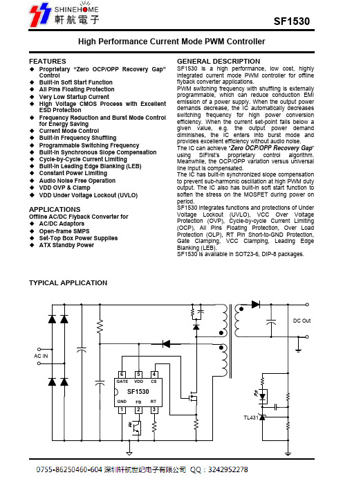
功能特性产品概述● 省去辅助绕组和VCC 供电回路 ● 集成高压启动电阻● Burst Mode 模式去除噪音影响 ● 低启动电流和低工作电流设计 ● 满足六级能效标准 ● 具备软启动功能● 内设抖频模式可降低EMI 干扰 ● 内置前沿消隐,内设自动重启功能 ● CS 开路保护,逐周期限流功能 ● 多种保护功能:输出二极管短路保护 内置过温保护 CS 短路保护RM6715S 是一种双绕组离线式开关电源管理芯片,内置高压MOSFET 及电流模式PWM+PFM 控制器,满足六级能效标准。
RM6715S 内置高压启动电阻,专利技术为VCC 供电,无需外部辅助绕组,节约设计成本。
RM6715S 芯片内置多种工作模式,在轻载情况下,芯片进入Burst mode 模式,消除变压器的音频噪音,提高转换效率;在待机模式下,电路进入打嗝模式,有效降低电路的待机功耗。
内部集成斜坡补偿模块,有利于CCM 模式下系统闭环反馈回路的稳定性,减小了输出纹波电压。
芯片内部集成多种异常状态保护功能。
在电路发生异常时,芯片进入保护状态并自动重启检测,异常解除,恢复正常输出。
应用领域SOP-8● 快速充电器 ● 适配器 ● 机顶盒电源产品规格产品名称封装类型丝印材料包装RM6715S SOP-8RM6715S无卤、无铅盘装典型应用结构框图极限参数参数数值范围单位DRAIN引脚耐压(V DGR) 650 VVCC引脚耐压(V GS) -0.3 to 40 V CS/FB引脚耐压(V CS,V FB) -0.3 to 7 V最小/最大结温点(T J) -40 to 150 ℃存储温度(T amb=25℃) -50 to 150 ℃焊接温度(10S)260 ℃电气特性(VCC=12V,TA=25℃。
除非另作说明)符号参数测试条件最小典型最大单位电源电压(VCC引脚)I_Vcc_Operation 工作电流FB=3V,CS=4V 2.0 2.5 3 mA I_Vcc_Burst Burst工作电流CS=0,FB=3.5V - 84 120 μA UVLO(ON) 欠压锁定开启电压10.3 10.8 11.3 V UVLO(OFF) 欠压锁定关断电压 6.5 7 7.5 V Vpull_up PMOS工作电压- 11 - V 负载反馈(FB引脚)V FB_open FB开路电压 4.8 5 - VI FB_short FB对地短路电流- 140 - uAPWM输入增益Apwm PWM输入增益- 12/7 - V/VΔV FB/ΔV CSMax duty cycle 最大占空比FB=3V,CS=0 77 80 83 %FB脚开环保护阈值电V TH_OLP3.5 3.7 3.9 V压Td_OLP OLP延迟触发时间45 50 55 mS 电流检测引脚(CS 引脚)Tsoftstart 软启动时间 1.5 2 2.5 mS T_blanking LEB时间280 330 400 nST D_OC过流检测控制延时从OCP发生到Gate关断时间-90 110 nSV TH_OC0占空比时CS阈值电压CS=3.3V,测试FB脚开环电压0.72 0.75 0.78 VV TH_OC_Clamp CS过流保护嵌位电压0.9 1 1.1 V 内置OTPOTP 140 150 160 ℃振荡器Fosc 振荡器频率CS=3.3V 60 65 70 KHz ΔF_OSC抖频幅度- ±6 - % F_shuffling 抖频控制频率- 32 - Hz F_BurstBurst模式下正常工作频率17 23 29 KHz MOSFET功率管B VDSS漏源击穿电压V GS=0V,I DS=250uA 650V VID漏端连续电流(T amb=25℃)5.0 AR DS(ON)静态漏源导通电阻V GS=10V,I DS=2A 1.8 Ω工作原理RM6715S 是一种内置高压MOSFET,离线式双绕组开关电源管理芯片,满足六级能效要求。
中国水产科学 2015年11月, 22(6): 1133-1141 Journal of Fishery Sciences of China研究论文收稿日期: 2015-03-13; 修订日期: 2015-04-20.基金项目: 科技基础性工作专项(2013FY110700); 山东省科技发展计划项目(2012GHY11531); 水科院基本科研业务费专项(2013A11); 泰山学者建设工程专项经费.作者简介: 李献儒(1989−), 男, 硕士研究生, 从事海洋生物学研究. E-mail: lxrzxn@ 通信作者: 柳淑芳, 研究员, 从事海洋分子生态学研究. E-mail: liusf@DOI: 10.3724/SP.J.1118.2015.15090DNA 条形码在鲱形目鱼类物种鉴定和系统进化分析中的应用李献儒1, 2, 柳淑芳2, 李达2, 3, 杜腾飞2, 3, 庄志猛21. 大连海洋大学 水产与生命学院, 辽宁 大连 116023;2. 中国水产科学研究院 黄海水产研究所, 山东省渔业资源与生态环境重点实验室, 山东 青岛 266071;3. 上海海洋大学 水产与生命学院, 上海 201306摘要: 采用PCR 特异性扩增获得中国近海鲱形目(Clupeiformes) 2科6属7种的48条线粒体CO I 基因序列, 结合从GenBank 筛选出的4科40属83种的CO I 基因序列225条, 对鲱形目鱼类的CO I 条形码基因特征、种内与种间遗传距离及其分子系统进化关系进行了分析, 探索了DNA 条形码技术在辅助鱼类物种鉴定和分类中的适应性。
结果表明, 4科41属90种273条CO I 基因序列的平均碱基组成为T: 28.3%、C: 28.3%、A: 24.2%、G: 19.2%, 碱基组成表现出明显偏倚性。
鲱形目鱼类种间的平均遗传距离为0.131, 种内平均遗传距离为0.003, 种间距离为种内距离的41倍; 系统学分析结果显示, 97.8%的鱼类在系统进化树上均为单系。
GP3SF1513F1应用资料一、 GP3SF1513F1应用原理图所有GP3SF1513F1的模块都具有,1PPS、GPS定位指示、天线检测功能。
只是适当的按以下电路连接即可。
适当的在VCC_3.3V-5V上加10uF,104,101的电容。
在VBAT_1.5V-5V上加104电容。
1.最简系统,接无源 GPS天线。
模块供电电压范围3.3V到5V。
模块备份电池电压范围1.5V到5V。
2.最简系统,接有源GPS天线。
天线电压2.85V,模块供电电压范围3.3V到 5V。
模块备份电池电压范围1.5V到5V。
3.接有源GPS天线。
天线电压3V-12V,由客户自己决定。
模块供电电压范围3.3V到5V。
模块备份电池电压范围1.5V到5V。
4.接有源GPS天线。
天线电压2.85V,外加LDO,可关断GPS模块,和天线电源。
模块备份电池电压范围1.5V到5V。
LDO输入电压3.3V到5V。
5.接有源GPS天线。
天线电压2.85V,外加LDO,可关断GPS模块,和天线电源。
模块备份电池3.3V由LDO充电 。
LDO输入电压3.3V到5V。
6.接有源GPS天线。
天线电压2.85V,模块备份电池电压范围1.5V到5V。
模块供电电压范围3.3V到5V。
带天线检测功能,通过串口会输出天线状态。
带GPS定位指示。
GPS 指示灯: GPS没定位:一直亮。
GPS 定位后:如下图的闪GPS模块UART天线状态输出:$GPTXT,01,01,02,ANTSTATUS=SHORT*6D$GPTXT,01,01,02,ANTSTATUS=OK*3B$GPTXT,01,01,02,ANTSTATUS=OPEN*2B二、 GP3SF1513F1 LAYOUT指引1.整个系统不需要分地。
GPS模块也不需要。
更不要用磁珠将GPS地分出来。
2.模块远离强干扰源。
如DSP、SRDAM、DCDC、OLED、TFT 等。
如有这些器件需要将它们屏蔽起来。
XP131A1330SRPower MOSFETPIN NUMBER PIN NAME FUNCTION1~3 S Source 4 G Gate 5~8 D DrainPARAMETERSYMBOL RA TINGS UNITS Drain-Source Voltage Vdss 20VGate-Source Voltage Vgss 8 V Drain Current (DC) Id 8 A Drain Current (Pulse) Idp 30 A Reverse Drain Current Idr8AChannel Power Dissipation * Pd 2.5 W Channel Temperature Tch 150 Storage Temperature RangeTstg-55~150GENERAL DESCRIPTIONThe XP131A1330SR is an N-channel Power MOSFET with low on-state resistance and ultra high-speed switching characteristicsBecause high-speed switching is possible, the IC can be efficiently set thereby saving energy. The small SOP-8 package makes high density mounting possible.APPLICATIONSNotebook PCsCellular and portable phones On-board power supplies Li-ion battery systemsFEATURESLow On-State Resistance :Rds(on)=0.03 (Vgs=4.5V) : Rds(on)=0.04 (Vgs=2.5V) : Rds(on)=0.07 (Vgs=1.5V) Ultra High-Speed SwitchingDriving Voltage : 1.5V N-Channel Power MOSFET DMOS StructurePackage : SOP-8PIN CONFIGURATION PIN ASSIGNMENTABSOLUTE MAXIMUM RATINGSEQUIVALENT CIRCUIT Ta = 25℃ETR1103_001PARAMETER SYMBOL CONDITIONS MIN.TYP .MAX.UNITS Drain Cut-Off Current Idss Vds=20V, Vgs=0V - - 10 A Gate-Source Leak Current Igss Vgs= 8V, Vds=0V - - 1 A Gate-Source Cut-Off Voltage Vgs(off) Id=1mA, Vds=10V 0.5 - 1.2 V Id=4A, Vgs=4.5V - 0.025 0.03 Id=4A, Vgs=2.5V - 0.030 0.040 Drain-Source On-State Resistance *Rds(on) Id=1A, Vgs=1.5V - 0.045 0.07 Forward Transfer Admittance *| Yfs |Id=4A, Vds=10V-22-SBody Drain Diode Forward VoltageVf If=8A, Vgs=0V - 0.85 1.1 VPARAMETER SYMBOL CONDITIONSMIN.TYP .MAX.UNITSThermal Resistance(Channel-Ambience)Rth (ch-a)Implement on a glass epoxyresin PCB- 50 - /WPARAMETER SYMBOL CONDITIONSMIN.TYP .MAX.UNITSInput Capacitance Ciss - 950 - pF Output Capacitance Coss - 430 - pF Feedback CapacitanceCrssVds=10V, Vgs=0Vf=1MHz - 180 - pFPARAMETER SYMBOL CONDITIONSMIN.TYP .MAX.UNITSTurn-On Delay Timetd (on)- 15 - ns Rise Time tr - 20 - ns Turn-Off Delay Timetd (off) - 80 - nsFall TimetfVgs=5V, Id=4AVdd=10V - 15 - ns ELECTRICAL CHARACTERISTICSDC CharacteristicsT a = 25℃* Effective during pulse test.T a = 25℃Switching CharacteristicsThermal CharacteristicsDynamic CharacteristicsT a = 25℃XP131A1330SRTYPICAL PERFORMANCECHARACTERISTICS(6) Gate-Source Cut-Off Voltage Variance vs. Ambient TemperatureTYPICAL PERFORMANCE CHARACTERISTICS (Continued)(11) Standardized transition Thermal Resistance vs. Pulse WidthXP131A1330SR。
User ManualV1.1 M aster Series Embedded SystemIntel ® Tiger Lake-UP3 Core-i/Celeron Processors Performance, Versatile, and Rugged & ReliablePREFACECopyright NoticeCopyright © 2016-2021 MiTAC Computing Technology Corporation (MiTAC Group). No part of this document may be reproduced, copied, translated, or transmitted in any form or by any means, electronic or mechanical, for any purpose, without the prior written permission of MiTAC Corp., Ltd. All information and specification provided in this manual are for reference only and remain subject to change without prior notice.DisclaimerWe reserve the right to make changes, without notice, to any product, including circuits and/or software described or contained in this manual in order to improve design and/or performance. We assume no responsibility or liability for the use of the described product(s) conveys no license or title under any patent, copyright, or masks work rights to these products, and make no representations or warranties that these products are free from patent, copyright, or mask work right infringement, unless otherwise specified. Applications that are described in this manual are for illustration purposes only. We make no representation or guarantee that such application will be suitable for the specified use without further testing or modification.Declaration of ConformitySafety InformationSafety PrecautionsFor your safety, please carefully read all the safety instructions before using the device. All cautions and warnings on the equipment should be noted. Keep this user manual for future reference.*Let service personnel to check the equipment in case any of the following problems appear:⏹The power cord or plug is damaged.⏹Liquid has penetrated into the equipment.⏹The equipment has been exposed to moisture.⏹The equipment does not work well or you cannot get it to work according to the user manual.⏹The equipment has been dropped and damaged.⏹The equipment has obvious signs of breakage on the surface.Ordering InformationPacking ListOptional Xpansion Modules and AccessoriesCONTENTSPREFACE 1CHAPTER 1: INTRODUCTION (10)1.1 Overview (10)1.2 Product Features (10)1.3 Hardware Specification (11)1.4 Mechanical Specification (15)1.5 System I/O Placement (16)CHAPTER 2: DIP SWITCH SETTING AND PIN DEFINITION (20)2.1 Jumper and Internal Connector Overall Placement (20)2.2 Jumper Setting (22)2.3 Internal Connector Pin Definition (24)2.4 External Connector Pin Definition (27)2.5 Xpansion Module MS-48CDN-DT10 (30)2.6 Xpansion Module MS-04LAN-M10 (34)2.7 Xpansion Module MS-01IGN-S10 (35)CHAPTER 3: SYSTEM SETUP (37)CHAPTER 4: BIOS SETUP (40)4.1 Main Page (40)4.2 Advanced Page (42)4.3 Evnet logs (58)4.4 Security Page (61)4.5 Boot Page (69)4.6 Save & Exit Page (73)1 INTRODUCTIONThis chapter provides the MP1-11TGS EmbeddedSystem product overview, including features,hardware and mechanical specifications.CHAPTER 1: INTRODUCTIONThis chapter provides the MP1-11TGS Embedded System product overview, including features, hardware, mechanical specifications, and I/O placement.1.1 OverviewMiTAC’s MP1-11TGS embedded system is the next generation embedded system with Intel® 11st Gen. (10nm+ manufacturing process) Tiger Lake-UP3 processor which integrates Iris Xeoutstanding graphic engine. The excellent graphic performance, performance processor, OCP/OVP power protection, and expandable design provide the solution for every complicated task and most types of application.1.2 Product FeaturesMP1-11TGS Embedded System offers the following features:⏹11st Generation Intel® Tiger Lake-UP3 Co re™ i7 / i5 / i3 / Celeron Processors⏹Integrated Intel® Iris Xe Graphic Engine⏹Quadruple Display with HDMI and DisplayPort Interface⏹Fan-less chassis and Expandable module design⏹Support COM/DIO/LAN/PoE via Xpansion Modules (Only for MP1-D model)⏹Support Power Ignition for Vehicle Application via Xpansion Module (Only for MP1-Dmodel)⏹8-24V Wide Power Voltage for MP1-11TGS; 12-36V Wide Power Voltage forMP1-11TGS-D⏹15W TDP: -40 ~ 70°C28W TDP: -40 ~ 60°C*with 0.7m/s Air Flow (w/ Extended Temp. SSD/mSATA/RAM)1.3 Hardware Specification*Notes1: Installation in Restricted Access Location (RAL)A restricted access location is a designated area within an incident area (High or Low temperature environment)With authorized people can enter for a period of time and for a specific purpose.1.Access can only be gained by service people or by users who have beeninstructed about the reasons for the Restrictions applied to the location and about any precautions that shall be taken.2.Access is through the use of a tool or lock and key, or other means ofsecurity, and is controlled by the authority Responsible for the location.*Notes2: Please make sure that the power consumption is in the spec of the power supply output capability from AC adaptor (72W or 120W). Please choose the suitable AC adaptor for your application.AC/DC 24V/3A, 72W 3PIN Terminal Block Power AdaptorAC/DC 24V/5A, 120W 3PIN Terminal Block Power Adaptor*Note3: The safety ambient operating temperature is 40 degree C if the external AC adapter model: EA10681V or EA11011M will be placed in thesame high temperature area with the embedded system.*Note4: In the PXE application, please install i219-LM driver in OS image inadvance before installing OS via PXE server.*Note5: CAUTION - Lithium battery is included in this embedded system. Please do not puncture, mutilate, or dispose of battery in fire. There will be danger of explosion if battery is incorrectly replaced. Replace only with the same or equivalent type recommended by manufacturer. Dispose of used battery according to manufacturer instructions and in accordance with your local regulations.1.4 Mechanical SpecificationMP1-11TGS⏹Mechanical Dimension: 210 mm x 150 mm x 63 mmMP1-11TGS-D⏹Mechanical Dimension: 210 mm x 150 mm x 103 mm1.5 System I/O PlacementMP1-11TGS⏹Front I/O:⏹Rear I/O:MP1-11TGS-D ⏹Front I/O:⏹Rear I/O:Xpansion Module (Optional) Configuration Table MP1-11TGSMP1-11TGS-D2 DIP SWITCH SETTING AND PIN DEFINITIONThis chapter provides information about how to set up thedip switch and use internal I/Os of MP1-11TGS EmbeddedSystem hardware.CHAPTER 2: DIP SWITCH SETTING AND PIN DEFINITIONThis chapter provides information about how to set up the dip switch, and use internal I/Os of MP1-11TGS Embedded System hardware.2.1 Jumper and Internal Connector Overall Placement2.2 Jumper Setting2.3 Internal Connector Pin Definition Standard ConnectorsSpecial Connectors2.4 External Connector Pin Definition⏹COM#1-3 (RS232) / COM#4 (RS232/422/485)⏹3-pin terminal block for DC Input*Only available in MP1-11TGS-D model.4-pin terminal block for DC Output (for MP1-11TGS-D model only)2.5 Xpansion Module MS-48CDN-DT10This Module MS-48CDN-DT10 consists of two parts, one is Serial COM, and the other is Digital IO function.Please see the guideline about how to set up this Module correctly.COM Port Settinga.LocationMS-48CDN-DT10 has total 4 x COM port. These COM ports can be set to beRS232/RS422/RS485 or powered RS232. There are 2 kinds of Xpansion COM driver.One is standard non-fixed COM port order driver, and the other one is fixed COM order driver.If what you install is fixed COM port order driver, the position will be as follows.b.Dip Switch Function(1)COM PID selection switchSet A-B; COM PID 0x1414 is determined by UART controller (default).Set B-C; COM PID 0x1415 is determined by EEPROM (setting for 2nd MS-48CDN-DT10).(2)Powered COM enable switch(3)Powered COM power source selection switch(4)COM Mode setting switch(5)COM Port PinoutDigital IO PortMS-48CDN-DT10 has total 8-bit GPIO, the position is as follows.This Module is a Giga LAN module, which supports four M12 type interfaces. Combined with MS-01PON-S10 to support PoE (typeA).M12 Code A LAN Module Pin definitionsThis Module MS-01IGN-S10 can detect vehicle ignition status and control the on/off delay time setting. This document is used to guide how to set up this power ignition module correctly.a.Locationb.Function✓Emergency reset buttonThis button is for engineering use only. The host will be reset when this button is pressed.✓Input power selection switchCommon car power supplies are DC 12V or 24V. Please set it according to yourenvironment.c.Delay Power On/Off Setting SwitchThis feature detects the ignition signal status and allows users to control the on/off delay time setting through DIP switch.SYSTEM SETUPThis chapter provides information about how to set up the MP1-11TGS Embedded System hardware installation. 3CHAPTER 3: SYSTEM SETUPThis chapter provides information about how to set up the MP1-11TGS Embedded System hardware installation.BIOS SETUPThis chapter provides information about how to set up BIOS and use BIOS menu items to adjust basic function settings. 4CHAPTER 4: BIOS SETUPThis chapter provides information about how to set up BIOS and use BIOS menu items to adjust basic function settings.4.1 Main Page4.2 Advanced Page4.2.1 Onboard Device4.2.2 CPU Configuration4.2.3 Trusted Computing4.2.4 NCT6126D Super IO Configuration4.2.5 Serial Port 1 Configuration。
GP3SF1513F1-S应用资料
一、 GP3SF1513F1–S应用原理图
所有GP3SF1513F1-S的模块都具有,1PPS、GPS定位指示。
只是适当的按以下电路连接即可。
适当的在VCC_3.3V-5V上加10uF,104,101的电容。
在VBAT_1.5V-5V上加104电容。
此封装GND脚多,可适当的几个脚不接。
但 第31、32、2、3脚必须接GND。
1.最简系统,接有源或无源GPS天线。
模块ANT脚(1脚)可输出2.85V 天线电源。
模块供电电压范围3.3V到5V。
模块备份电池电压范围1.5V到5V。
2.接有源或无源GPS天线。
天线电压3-12V,由客户自己决定。
模块供电电压范围3.3V 到 5V。
模块备份电池电压范围1.5V到5V。
3.接有源或无源GPS天线。
天线电压2.85V,外加LDO,可关断GPS模块,和天线电源。
模块备份电池3.3V,由LDO充电。
LDO输入电压3.3V到5V。
带GPS定位指示。
4.接有源或无源GPS天线。
天线电压2.85V,外加LDO,可关断GPS模块,和天线电源。
模块备份电池电压范围1.5V到5V。
LDO输入电压3.3V到5V。
带GPS定位指示。
GPS 指示灯: GPS没定位:一直亮。
GPS 定位后:如下图的闪
GPS模块UART天线状态输出:
$GPTXT,01,01,02,ANTSTATUS=SHORT*6D
$GPTXT,01,01,02,ANTSTATUS=OK*3B
$GPTXT,01,01,02,ANTSTATUS=OPEN*2B
二、 GP3SF1513F1-S LAYOUT指引
1.整个系统不需要分地。
GPS模块也不需要。
更不要用磁珠将GPS地分出来。
2.模块远离强干扰源。
如DSP、SRDAM、DCDC、OLED、TFT 等。
如有这些器件需要将它们屏蔽起来。
3.模块1脚到天线或天线座采用50Ω阻抗的微带线。
微带线越短越好。
不要超过10mm,
微带线下的地层尽量大。
微带线下不要有走线,即使第三层或第四层。
如下图:
如:板材 FR4,H=0.1mm,W=0.17mm(其他参数不是很明显影响)
4.所有的馈线,虽然标明是50Ω。
它是对信号有损耗的。
尽量缩短馈线的长度。
5.模块下面尽量不要走线。
那些IO线是带有主CPU CLK的分量,带有辐射的。
6.用的有源或无源天线中的陶瓷天线尽量采用大、厚尺寸的。
如下图:
7.整机系统的EMI直接影响GPS的接收性能。
做好整机EMI是GPS性能好的前提。
三、 GP3SF1513F1-S性能指标
1.GP3SF1513F1-S电气指标
模块供电 3.3V – 5V
工作电压
备份电源 1.5V – 5V
ANT输出 2.85V
搜索 44mA
工作电流
定位后 33mA
后备电池工作电流(Ibat) 15uA
2.GPS性能指标
Chip SiRF Star III GSC3F/LP-7979
Frequency L1 1575.42MHz, C/A code
Channels 20
Update Rate 1Hz
Tracking -159dBm Sensitivity
Cold Start -144dBm
Host Start (Open Sky) <2s
Acquisition Time
Hot Start (Indoor) <15s
Cold Start (Open Sky) 38s(Typical)
RMS)
Autonomous <10m(2D Position Accuracy
RMS)
SBAS <5m(2D Max. Altitude <60,000ft
Max. Velocity <1,000knots
NMEA 0183 ver 3.0 4800bps, 8data bits, no parity, 1
stop bit(default)
1Hz: GGA,GLL,GSA,RMC,VTG Protocol Support
0.2Hz: GSV1
SiRF Binary 38400bps, 8data bits, no parity, 1
stop bits
1Hz GSV at 9600 bps.。