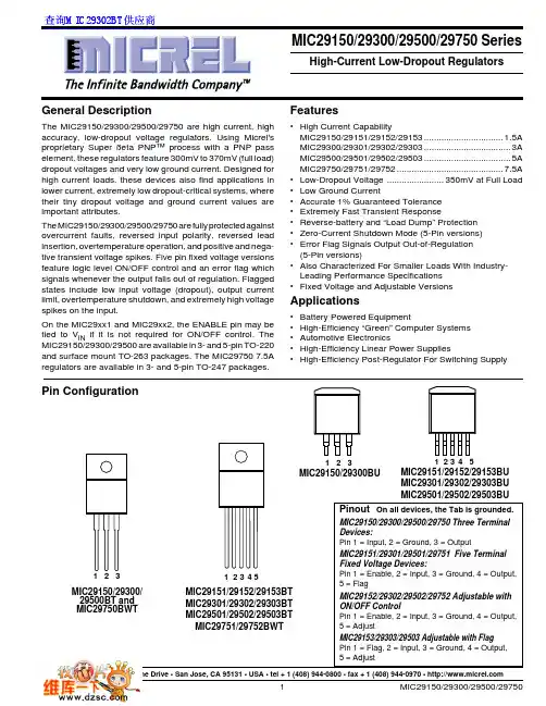
General DescriptionThe MIC29150/29300/29500/29750 are high current, high accuracy, low-dropout voltage regulators. Using Micrel's proprietary Super ßeta PNP™ process with a PNP pass element, these regulators feature 300mV to 370mV (full load) dropout voltages and very low ground current. Designed for high current loads, these devices also find applications in lower current, extremely low dropout-critical systems, where their tiny dropout voltage and ground current values are important attributes.The MIC29150/29300/29500/29750 are fully protected against overcurrent faults, reversed input polarity, reversed lead insertion, overtemperature operation, and positive and nega-tive transient voltage spikes. Five pin fixed voltage versions feature logic level ON/OFF control and an error flag which signals whenever the output falls out of regulation. Flagged states include low input voltage (dropout), output current limit, overtemperature shutdown, and extremely high voltage spikes on the input.On the MIC29xx1 and MIC29xx2, the ENABLE pin may be tied to V IN if it is not required for ON/OFF control. The MIC29150/29300/29500 are available in 3- and 5-pin TO-220 and surface mount TO-263 packages. The MIC29750 7.5A regulators are available in 3- and 5-pin TO-247 packages.Features•High Current CapabilityMIC29150/29151/29152/29153................................1.5A MIC29300/29301/29302/29303...................................3A MIC29500/29501/29502/29503...................................5A MIC29750/29751/29752...........................................7.5A •Low-Dropout Voltage.......................350mV at Full Load •Low Ground Current•Accurate 1% Guaranteed Tolerance•Extremely Fast Transient Response•Reverse-battery and “Load Dump” Protection•Zero-Current Shutdown Mode (5-Pin versions)•Error Flag Signals Output Out-of-Regulation(5-Pin versions)•Also Characterized For Smaller Loads With Industry-Leading Performance Specifications•Fixed Voltage and Adjustable Versions Applications•Battery Powered Equipment•High-Efficiency “Green” Computer Systems •Automotive Electronics•High-Efficiency Linear Power Supplies•High-Efficiency Post-Regulator For Switching SupplyMIC29150/29300/29500/29750MicrelPart Number Temp. Range*Volts Current Package MIC29500-3.3BT –40 to +125°C 3.3 5.0A TO-220MIC29500-5.0BT –40 to +125°C 5.0 5.0A TO-220MIC29501-3.3BT –40 to +125°C 3.3 5.0A TO-220-5MIC29501-5.0BT –40 to +125°C 5.0 5.0A TO-220-5MIC29501-3.3BU –40 to +125°C 3.3 5.0A TO-263-5MIC29501-5.0BU –40 to +125°C 5.0 5.0A TO-263-5MIC29502BT –40 to +125°C Adj 5.0A TO-220-5MIC29502BU –40 to +125°C Adj 5.0A TO-263-5MIC29503BT –40 to +125°C Adj 5.0A TO-220-5MIC29503BU –40 to +125°C Adj 5.0A TO-263-5MIC29750-3.3BWT –40 to +125°C 3.37.5A TO-247-3MIC29750-5.0BWT –40 to +125°C 5.07.5A TO-247-3MIC29751-3.3BWT –40 to +125°C 3.37.5A TO-247-5MIC29751-5.0BWT –40 to +125°C 5.07.5A TO-247-5MIC29752BWT–40 to +125°CAdj7.5ATO-247-5Ordering InformationPart Number Temp. Range*Volts Current Package MIC29150-3.3BT –40 to +125°C 3.3 1.5A TO-220MIC29150-4.2BT –40 to +125°C 4.2 1.5A TO-220MIC29150-5.0BT –40 to +125°C 5.0 1.5A TO-220MIC29150-12BT –40 to +125°C 12 1.5A TO-220MIC29150-3.3BU –40 to +125°C 3.3 1.5A TO-263MIC29150-5.0BU –40 to +125°C 5.0 1.5A TO-263MIC29150-12BU –40 to +125°C 12 1.5A TO-263MIC29151-3.3BT –40 to +125°C 3.3 1.5A TO-220-5MIC29151-5.0BT –40 to +125°C 5.0 1.5A TO-220-5MIC29151-12BT –40 to +125°C 12 1.5A TO-220-5MIC29151-3.3BU –40 to +125°C 3.3 1.5A TO-263-5MIC29151-5.0BU –40 to +125°C 5.0 1.5A TO-263-5MIC29151-12BU –40 to +125°C 12 1.5A TO-263-5MIC29152BT –40 to +125°C Adj 1.5A TO-220-5MIC29152BU –40 to +125°C Adj 1.5A TO-263-5MIC29153BT –40 to +125°C Adj 1.5A TO-220-5MIC29153BU –40 to +125°C Adj 1.5A TO-263-5MIC29300-3.3BT –40 to +125°C 3.3 3.0A TO-220MIC29300-5.0BT –40 to +125°C 5.0 3.0A TO-220MIC29300-12BT –40 to +125°C 12 3.0A TO-220MIC29300-3.3BU –40 to +125°C 3.3 3.0A TO-263MIC29300-5.0BU –40 to +125°C 5.0 3.0A TO-263MIC29300-12BU –40 to +125°C 12 3.0A TO-263MIC29301-3.3BT –40 to +125°C 3.3 3.0A TO-220-5MIC29301-5.0BT –40 to +125°C 5.0 3.0A TO-220-5MIC29301-12BT –40 to +125°C 12 3.0A TO-220-5MIC29301-3.3BU –40 to +125°C 3.3 3.0A TO-263-5MIC29301-5.0BU –40 to +125°C 5.0 3.0A TO-263-5MIC29301-12BU –40 to +125°C 12 3.0A TO-263-5MIC29302BT –40 to +125°C Adj 3.0A TO-220-5MIC29302BU –40 to +125°C Adj 3.0A TO-263-5MIC29303BT –40 to +125°C Adj 3.0A TO-220-5MIC29303BU–40 to +125°CAdj3.0ATO-263-5MIC29xx0 versions are 3-terminal fixed voltage devices.MIC29xx1 are fixed voltage devices with ENABLE and ERROR flag. MIC29xx2 are adjustable regulators with ENABLE control.MIC29xx3 are adjustables with an ERROR flag.* Junction TemperatureMIC29150/29300/29500/29750MicrelAbsolute Maximum RatingsPower Dissipation ....................................Internally Limited Lead Temperature (Soldering, 5 seconds)................260°C Storage Temperature Range ...................–65°C to +150°C Input Supply Voltage (Note 1).......................–20V to +60VOperating RatingsOperating Junction Temperature .............–40°C to +125°C Maximum Operating Input Voltage...............................26V TO-220 θJC ..............................................................2°C/W TO-263 θJC ..............................................................2°C/W TO-247 θJC ...........................................................1.5°C/WElectrical CharacteristicsAll measurements at T J = 25°C unless otherwise noted. Bold values are guaranteed across the operating temperature range.Adjustable versions are programmed to 5.0V.Parameter Condition Min TypMax Units Output VoltageI O = 10mA–11%10mA ≤ I O ≤ I FL , (V OUT + 1V) ≤ V IN ≤ 26V (Note 2)–22%Line Regulation I O = 10mA, (V OUT + 1V) ≤ V IN ≤ 26V0.060.5%Load Regulation V IN = V OUT + 5V, 10mA ≤ I OUT ≤ I FULL LOAD (Note 2, 6)0.21%∆V O Output Voltage (Note 6)20100ppm/°C∆TTemperature Coef.Dropout Voltage∆V OUT = – 1%, (Note 3)MIC29150I O = 100mA80200mVI O = 750mA 220I O = 1.5A350600MIC29300I O = 100mA80175I O = 1.5A 250I O = 3A370600MIC29500I O = 250mA125250I O = 2.5A 250I O = 5A370600MIC29750I O = 250mA80200I O = 4A 270I O = 7.5A 425600Ground Current MIC29150I O = 750mA, V IN = V OUT + 1V 820mA I O = 1.5A22MIC29300I O = 1.5A, V IN = V OUT + 1V 1035mA I O = 3A37MIC29500I O = 2.5A, V IN = V OUT + 1V 1550mA I O = 5A70MIC29750I O = 4A, V IN = V OUT + 1V 3575mAI O = 7.5A120I GNDDO Ground Pin V IN = 0.5V less than specified V OUT . I OUT = 10mA Current at DropoutMIC291500.9mA MIC29300 1.7mA MIC29500 2.1mA MIC29750 3.1mA Current LimitMIC29150V OUT = 0V (Note 4) 2.1 3.5A MIC29300V OUT = 0V (Note 4) 4.5 5.0A MIC29500V OUT = 0V (Note 4)7.510.0A MIC29750V OUT = 0V (Note 4)9.515A e n , Output Noise C L = 10µF 400µV (rms)Voltage(10Hz to 100kHz)C L = 33µF260I L = 100mAGround Current in ShutdownMIC29150/1/2/3 onlyV EN = 0.4V210µA 30µAMIC29150/29300/29500/29750MicrelElectrical Characteristics (Continued)ReferenceMIC29xx2/MIC29xx3Parameter ConditionsMin Typical Max Units Reference Voltage1.228 1.2401.252V 1.2151.265V max Reference Voltage (Note 8)1.2031.277V Adjust Pin 4080nABias Current 120Reference Voltage (Note 7)20ppm/°CTemperature CoefficientAdjust Pin Bias0.1nA/°CCurrent Temperature CoefficientFlag Output (Error Comparator) MIC29xx1/29xx3Output Leakage V OH = 26V0.011.00µACurrent 2.00Output Low Device set for 5V. V IN = 4.5V 220300mVVoltageI OL = 250µA400Upper Threshold Device set for 5V (Note 9)4060mVVoltage25Lower Threshold Device set for 5V (Note 9)7595mVVoltage 140Hysteresis Device set for 5V (Note 9)15mVENABLE Input Input Logic Voltage VLow (OFF)0.8High (ON) 2.4Enable Pin V EN = 26V 100600µAInput Current750V EN =0.8V1µA2Regulator Output (Note 10)10µACurrent in Shutdown500MIC29xx1/MIC29xx2MIC29150/29300/29500/29750Micrel NotesNote 1:Maximum positive supply voltage of 60V must be of limited duration (<100msec) and duty cycle (≤1%). The maximum continuous supply voltage is 26V.Note 2:Full Load current (I FL) is defined as 1.5A for the MIC29150, 3A for the MIC29300, 5A for the MIC29500, and 7.5A for the MIC29750 families. Note 3:Dropout voltage is defined as the input-to-output differential when the output voltage drops to 99% of its nominal value with V OUT + 1V applied to V INNote 4:V IN = V OUT (nominal) + 1V. For example, use V IN = 4.3V for a 3.3V regulator or use 6V for a 5V regulator. Employ pulse-testing procedures to minimize temperature rise.Note 5:Ground pin current is the regulator quiescent current. The total current drawn from the source is the sum of the load current plus the ground pin current.Note 6:Output voltage temperature coefficient is defined as the worst case voltage change divided by the total temperature range.Note 7:Thermal regulation is defined as the change in output voltage at a time T after a change in power dissipation is applied, excluding load or line regulation effects. Specifications are for a 200mA load pulse at V IN = 20V (a 4W pulse) for T = 10ms.Note 8:V REF≤ V OUT≤ (V IN – 1 V), 2.3V ≤ V IN≤ 26V, 10mA < I L≤ I FL, T J ≤ T J MAX.Note 9:Comparator thresholds are expressed in terms of a voltage differential at the Adjust terminal below the nominal reference voltage measured at 6V input. To express these thresholds in terms of output voltage change, multiply by the error amplifier gain = V OUT /V REF = (R1 + R2)/R2. For example, at a programmed output voltage of 5V, the Error output is guaranteed to go low when the output drops by 95 mV x 5V/1.240 V = 384 mV. Thresholds remain constant as a percent of V OUT as V OUT is varied, with the dropout warning occurring at typically 5% below nominal,7.7% guaranteed.Note 10:V EN≤ 0.8V and V IN≤ 26V, V OUT = 0.Note 11:When used in dual supply systems where the regulator load is returned to a negative supply, the output voltage must be diode clamped to ground.Block DiagramENINFLAG†*Feedback network in fixed versions only†Adjustable version onlyTypical ApplicationsFigure 1. Fixed output voltage.Figure 2. Adjustable output voltage configuration. For 5V ± 3.3V ± 1% @ 5AV OUT = 1.240V× [1 + (R1 / R2)]V IN V OUTMIC29150/29300/29500/29750Micrel Typical Characteristics MIC2915xMIC29150/29300/29500/29750MicrelMIC29150/29300/29500/29750Micrel Typical Characteristics MIC2930xMIC29150/29300/29500/29750MicrelMIC29150/29300/29500/29750Micrel Typical Characteristics MIC2950xTypical Characteristics MIC2975xApplications InformationThe MIC29150/29300/29500/29750 are high performance low-dropout voltage regulators suitable for all moderate to high-current voltage regulator applications. Their 300mV to 400mV dropout voltage at full load make them especially valuable in battery powered systems and as high efficiency noise filters in “post-regulator ” applications. Unlike older NPN-pass transistor designs, where the minimum dropout voltage is limited by the base-emitter voltage drop and collector-emitter saturation voltage, dropout performance of the PNP output of these devices is limited merely by the low V CE saturation voltage.A trade-off for the low dropout voltage is a varying base drive requirement. But Micrel ’s Super ßeta PNP ™ process re-duces this drive requirement to merely 1% of the load current.The MIC29150–29750 family of regulators is fully protected from damage due to fault conditions. Current limiting is provided. This limiting is linear; output current under overload conditions is constant. Thermal shutdown disables the de-vice when the die temperature exceeds the 125°C maximum safe operating temperature. Transient protection allows de-vice (and load) survival even when the input voltage spikes between –20V and +60V. When the input voltage exceeds about 35V to 40V, the overvoltage sensor temporarily dis-ables the regulator. The output structure of these regulators allows voltages in excess of the desired output voltage to be applied without reverse current flow. MIC29xx1 and MIC29xx2versions offer a logic level ON/OFF control: when disabled,the devices draw nearly zero current.An additional feature of this regulator family is a common pinout: a design ’s current requirement may change up or down yet use the same board layout, as all of these regulators have identical pinouts.OUTV Figure 3. Linear regulators require only two capacitorsfor operation.Thermal DesignLinear regulators are simple to use. The most complicated design parameters to consider are thermal characteristics.Thermal design requires the following application-specific parameters:• Maximum ambient temperature, T A • Output Current, I OUT • Output Voltage, V OUT • Input Voltage, V INFirst, we calculate the power dissipation of the regulator from these numbers and the device parameters from this datasheet.P I 1.01V V D OUT IN OUT=−()Where the ground current is approximated by 1% of I OUT .Then the heat sink thermal resistance is determined with this formula:θθθSA J MAX ADJC CST T P =−−+()Where T J MAX ≤ 125°C and θCS is between 0 and 2°C/W.The heat sink may be significantly reduced in applications where the minimum input voltage is known and is large compared with the dropout voltage. Use a series input resistor to drop excessive voltage and distribute the heat between this resistor and the regulator. The low dropout properties of Micrel Super ßeta PNP regulators allow very significant reductions in regulator power dissipation and the associated heat sink without compromising performance.When this technique is employed, a capacitor of at least 0.1µF is needed directly between the input and regulator ground.Please refer to Application Note 9 and Application Hint 17 for further details and examples on thermal design and heat sink specification.Capacitor RequirementsFor stability and minimum output noise, a capacitor on the regulator output is necessary. The value of this capacitor is dependent upon the output current; lower currents allow smaller capacitors. MIC29150—29750 regulators are stable with the following minimum capacitor values at full load:Device Full Load Capacitor MIC29150..............................10µF MIC29300..............................10µF MIC29500..............................10µF MIC29750..............................22µFThis capacitor need not be an expensive low ESR type:aluminum electrolytics are adequate. In fact, extremely low ESR capacitors may contribute to instability. Tantalum ca-pacitors are recommended for systems where fast load transient response is important.Where the regulator is powered from a source with a high AC impedance, a 0.1µF capacitor connected between Input and GND is recommended. This capacitor should have good characteristics to above 250kHz.Minimum Load CurrentThe MIC29150–29750 regulators are specified between fi-nite loads. If the output current is too small, leakage currents dominate and the output voltage rises. The following mini-mum load current swamps any expected leakage current across the operating temperature range:Device Minimum LoadMIC29150....................................................5mAMIC29300....................................................7mAMIC29500..................................................10mAMIC29750..................................................10mA Adjustable Regulator DesignV OUT = 1.235V× [1 + (R1 / R2)]V IN V OUTFigure 4. Adjustable Regulator with ResistorsThe adjustable regulator versions, MIC29xx2 and MIC29xx3, allow programming the output voltage anywhere between 1.25V and the 26V maximum operating rating of the family.Two resistors are used. Resistors can be quite large, up to 1MΩ, because of the very high input impedance and low bias current of the sense comparator: The resistor values are calculated by:R RV1.24012OUT=−1Where V O is the desired output voltage. Figure 4 shows component definition. Applications with widely varying load currents may scale the resistors to draw the minimum load current required for proper operation (see above).Error FlagMIC29xx1 and MIC29xx3 versions feature an Error Flag, which looks at the output voltage and signals an error condition when this voltage drops 5% below its expected value. The error flag is an open-collector output that pulls low under fault conditions. It may sink 10mA. Low output voltage signifies a number of possible problems, including an over-current fault (the device is in current limit) and low input voltage. The flag output is inoperative during overtempera-ture shutdown conditions.Enable InputMIC29xx1 and MIC29xx2 versions feature an enable (EN) input that allows ON/OFF control of the device. Special design allows “zero” current drain when the device is dis-abled—only microamperes of leakage current flows. The EN input has TTL/CMOS compatible thresholds for simple inter-facing with logic, or may be directly tied to ≤ 30V. Enabling the regulator requires approximately 20µA of current.Package Information3-Lead TO-220 (T)±0.005±0.005 0.100±0.01+0.004–0.0080.065±20°±2°3-Lead TO-263 (U)MOUNTING HOLE0.200(5.080)BSC3-Lead TO-247 (WT)inch(mm)Dimensions:5-Lead TO-220 (T)0.067±±0.005±0.005 0.100±0.01+0.004–0.0080.065±20°±2°5-Lead TO-263 (U)MOUNTING HOLE5-Lead TO-247 (WT)MICREL INC.1849 FORTUNE DRIVE SAN JOSE, CA95131USATEL + 1 (408) 944-0800 FAX + 1 (408) 944-0970 WEB This information is believed to be accurate and reliable, however no responsibility is assumed by Micrel for its use nor for any infringement of patents or。