CD40192BC
- 格式:doc
- 大小:1.02 MB
- 文档页数:8
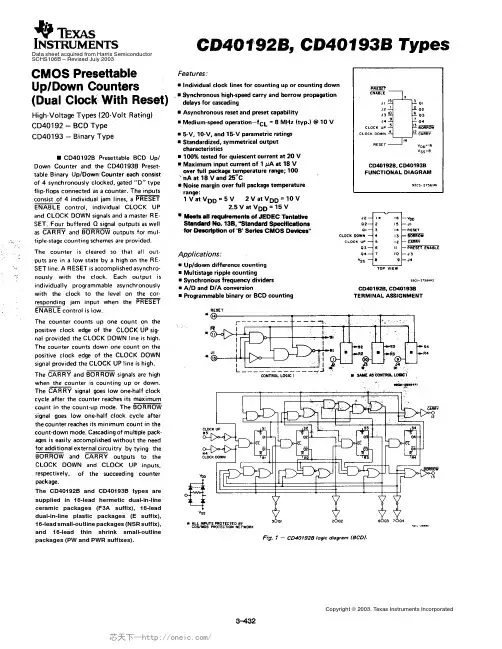
October 1987Revised January 1999CD40192BC • CD40193BCSynchronous 4-Bit Up/Down Decade Counter •Synchronous 4-Bit Up/Down Binary Counter CD40192BC•CD40193BCCounterGeneral DescriptionThe CD40192BC and CD40193BC up/down counters are monolithic complementary MOS (CMOS) integrated cir-cuits. The CD40192BC is a BCD counter, while the CD40193BC is a binary counter.Counting up and counting down is performed by two count inputs, one being held HIGH while the other is clocked. The outputs change on the positive-going transition of this clock.These counters feature preset inputs that are enabled when load is a logical “0” and a clear which forces all out-puts to “0” when it is at logical “1”. The counters also have carry and borrow outputs so that they can be cascaded using no external circuitry. All inputs are protected against damage due to static dis-charge by clamps to V DD and V SS.Features■Wide supply voltage range: 3V to 15V■High noise immunity: 0.45 V DD (typ.)■Low power TTL compatibility: Fan out of 2 driving 74L or 1 driving 74LS■Carry and borrow outputs for easy expansion to N-bit by cascading■Asynchronous clear■Equivalent to: MM74C192 and MM74C193Synchronous 4-BitOrdering Code:Order Number Package Number Package DescriptionCD40192BCN N16E 16-Lead Plastic Dual-In-Line Package (PDIP), JEDEC MS-001, 0.300” WideCD40193BCN N16E 16-Lead Plastic Dual-In-Line Package (PDIP), JEDEC MS-001, 0.300” WideCD40193BCM M16A 16-Lead Small Outline Integrated Circuit (SOIC), JEDEC MS-012, 0.150” Narrow Body Devices also available in Tape and Reel. Specify by appending suffix letter “X” to the ordering code.Connection Diagram Cascading PackagesPin Assignments for DIP and SOICTop ViewUp/Down Decade Counter • Synchronous 4-Bit Up/Down Binary© 1999 Fairchild Semiconductor Corporation DS005988.prf C D 40192B C • C D 40193B CBlock DiagramsCD40192BC Synchronous 4-Bit Up/Down Decade CounterCD40193BC Synchronous 4-Bit Up/Down Binary Counter2Absolute Maximum Ratings (Note 1)Recommended Operating(Note 2)Conditions (Note 2)DC Supply Voltage (V DD ) -0.5 to +18 V DC DC Supply Voltage (V DD )3 to 15 V DCInput Voltage (V IN )-0.5 to V DD +0.5 V DCInput Voltage (V IN )0 to V DD V DCStorage Temperature Range (T S ) -65︒C to +150︒C Operating Temperature Range (T A )CD40192BC, CD40193BC -40︒C to +85︒CPower Dissipation (P D )Note 1: “Absolute Maximum Ratings” are those values beyond which the Dual-In-Line700 mWsafety of the device cannot be guaranteed. They are not meant to imply Small Outline 500 mWthat the devices should be operated at these limits. The “Recommended Lead Temperature (T L )Operating Conditions ” and Electrical Characteristics tables provide condi -tions for actual device operation.(Soldering, 10 seconds)260︒CNote 2: V SS = 0V unless otherwise specified.DC Electrical Characteristics (Note 3)SymbolParameterConditions-40︒C+25︒C+85︒CUnitsMinMaxMinTypMaxMinMaxIDD Quiescent Device V DD = 5V, V IN = V DD or V SS2020150 μACurrentV DD = 10V, V IN = V DD or V SS 40 40 300 μAV DD = 15V, V IN = V DD or V SS8080600 μA VOLLOW Level V DD = 5V0.050.050.05 V Output VoltageV DD = 10V 0.05 0.05 0.05 VV DD = 15V0.050.050.05V VOHHIGH Level V DD = 5V4.954.954.95V Output VoltageV DD = 10V 9.959.95 9.95 VV DD = 15V14.9514.9514.95VVILLOW Level V DD = 5V, V O = 0.5V or 4.5V1.51.51.5 V Input VoltageV DD = 10V, V O = 1V or 9V3.0 3.0 3.0 VV DD = 15V, V O = 1.5V or 13.5V4.04.04.0V VIHHIGH Level V DD = 5V, V O = 0.5V or 4.5V3.53.53.5V Input VoltageV DD = 10V, V O = 1V or 9V7.0 7.0 7.0 VV DD = 15V, V O = 1.5V or 13.5V11.011.011.0V IOLLOW Level Output V DD = 5V, V O = 0.4V0.520.440.880.36mA Current (Note 4)V DD = 10V, V O = 0.5V 1.3 1.1 2.25 0.9 mAV DD = 15V, V O = 1.5V3.63.08.82.4mA IOHHIGH Level Output V DD = 5V, V O = 4.6V-0.52-0.44-0.88-0.36mA Current (Note 4)V DD = 10V, V O = 9.5V -1.3 -1.1 -2.25 -0.9 mAV DD = 15V, V O = 13.5V-3.6-3.0-8.8-2.4mA IINInput CurrentV DD = 15V, V IN = 0V-0.3 -10-5-0.3 -1.0 μAV DD = 15V, V IN = 15V0.310-50.31.0μANote 3: AC Parameters are guaranteed by DC correlated testing.Note 4: I OH and I OL are tested one output at a time.CD40192BC • CD40193BC3C D 40192B C • C D 40193B CAC Electrical Characteristics (Note 3)T A = 25︒C, C L = 50 pF, R L = 200 k Ω, input t r = t f = 20 ns, unless otherwise specified.SymbolParameterConditionsMinTypMaxUnitstPHLor tPLH Propagation Delay Time V DD = 5V250 400 ns from Count Up or V DD = 10V 100 160 ns Count Down to Q V DD = 15V 80 130 ns tPHLor tPLHPropagation Delay Time V DD = 5V120 200 ns from Count Up to CarryV DD = 10V 50 80 nsV DD = 15V 40 65 ns tPHLor tPLHPropagation Delay Time V DD = 5V120 200 ns from Count Down V DD = 10V 50 80 ns to Borrow V DD = 15V 40 65 ns tSUTime Prior to Load V DD = 5V100 160 ns That Data Must V DD = 10V 30 50 ns Be PresentV DD = 15V 25 40 ns tPHLPropagation Delay Time V DD = 5V130 220 ns from Clear to QV DD = 10V 60 100 nsV DD = 15V 50 80 ns tPLHor tPHLPropagation Delay Time V DD = 5V300 480 ns from Load to QV DD = 10V 120 190 nsV DD = 15V 95 150 ns tTLHor tTHLOutput Transition TimeV DD = 5V100 200 ns V DD = 10V 50 100 nsV DD = 15V4080ns fCLMaximum Count FrequencyV DD = 5V 2.5 4MHz V DD = 10V 6 10 MHzV DD = 15V 7.5 12.5MHz trCLor tfCLMaximum Count Rise V DD = 5V 15μs or Fall TimeV DD = 10V 5 μsV DD = 15V 1μstWH, tWLMinimum Count Pulse V DD = 5V120 200 ns WidthV DD = 10V 35 80 nsV DD = 15V 28 65 ns tWHMinimum Clear V DD = 5V300 480 ns Pulse WidthV DD = 10V 120 190 nsV DD = 15V 95 150 ns tWLMinimum Load V DD = 5V100 160 ns Pulse WidthV DD = 10V 40 65 nsV DD = 15V 32 55 ns CINAverage Input CapacitanceLoad and Data57.5pFInputs (A,B,C,D)Count Up, Count 10 15pFDown and ClearCPD Power Dissipation Capacity (Note 5)100pFNote 5: C PD determines the no load AC power consumption of any CMOS device. For complete explanation, see Family Characteristics application note, AN-90.4Timing DiagramsCD40192BCSequence:1. Clear outputs to zero.2. Load (preset) to BCD seven.3. Count up to eight, nine, carry, zero, one and two.4. Count down to one, zero, borrow, nine, eight and seven.CD40193BCSequence:1. Clear outputs to zero.2. Load (preset) to binary thirteen.3. Count up to fourteen, fifteen, carry, zero, one and two.4. Count down to one, zero, borrow, fifteen, fourteen and thirteen.CD40192BC • CD40193BC5C D 40192B C • C D 40193B CPhysical Dimensions inches (millimeters) unless otherwise noted16-Lead Small Outline Integrated Circuit (SOIC), JEDEC MS-012, 0.150” Narrow BodyPackage Number M16A6Physical Dimensions inches (millimeters) unless otherwise noted (Continued)16-Lead Plastic Dual-In-Line Package (PDIP), JEDEC MS-001, 0.300” WidePackage Number N16ELIFE SUPPORT POLICYFAIRCHILD’S PRODUCTS ARE NOT AUTHORIZED FOR USE AS CRITICAL COMPONENTS IN LIFE SUPPORTDEVICES OR SYSTEMS WITHOUT THE EXPRESS WRITTEN APPROVAL OF THE PRESIDENT OF FAIRCHILD SEMICONDUCTOR CORPORATION. As used herein:1. Life support devices or systems are devices or systems2. A critical component in any component of a life supportwhich, (a) are intended for surgical implant into the device or system whose failure to perform can be rea- body, or (b) support or sustain life, and (c) whose failure sonably expected to cause the failure of the life supportto perform when properly used in accordance with device or system, or to affect its safety or effectiveness.instructions for use provided in the labeling, can be rea-sonably expected to result in a significant injury to the user.Fairchild does not assume any responsibility for use of any circuitry described, no circuit patent licenses are implied and Fairchild reserves the right at any time without notice to change said circuitry and specifications.。