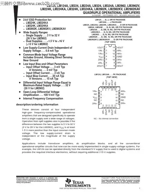
LM324中文PDF资料
- 格式:pdf
- 大小:324.61 KB
- 文档页数:7
— VO(P)=1V 11V Ω VCC=30V,RL=2K Ω VCC=30V,RL=10K ≥ Ω VCC=5V,RL 10K — f=1KHZ 20KHZ
输出电流
ISOURCE
VI(+)=1V,VI(-)=0V VCC=15V,VO(P)=2V
VI(+)=0V,VI(-)=1V
ISINK
VCC=15V,VO(P)=2V
)
工作温度范围
贮存温度范围
符号
Vcc VI(DIFF)
VI
TOPR TSTG
第一价值网(IC网络超市)
数值
± 或 18 36 ±32
— -0.3 +32 连续 —0 +70
— -65 +150
单位
V V V
℃ ℃
电参数(除非特别说明,Vcc=5.0V,VEE=GND,TA=25℃)
参数
输入失调电压 输入失调电流 输入偏置电流 输入共模电压范围 电源电流 大信号电压增益
VCC=30V
≥ Ω VCC=15V,RL 2K — VO(P)=1V 11V Ω VCC=30V,RL=2K Ω VCC=30V,RL=10K ≥ Ω VCC=5V,RL 10K
输出电流
ISOURCE
VI(+)=1V,VI(-)=0V VCC=15V,VO(P)=2V
VI(+)=0V,VI(-)=1V
图图图图图 (mA)
10
102
Io (mA)
40
输输输输20
0 -50 -25
0
25
50
温温 (温)
75
100
第一价值网(IC网络超市) 5
www.ic-jiazhi.com
REV 1.2 2004.7.20
LM324 双极型线性集成电路
外形尺寸图
第一价值网(IC网络超市)
差模输入电压
ISINK VI(DIFF)
VCC=15V,VO(P)=2V
第一价值网(IC网络超市)
最小值 典型值 最大值 单 位
9.0
mV
7.0
μV/℃
150
nA
10
℃ pA/
40
500
nA
0
VCC-2.0
V
15
V/mV
26
V
27
28
5
20
mV
10
30
mA
5
9
mA
VCC
V
管脚排列图
第一价值网(IC网络超市) 3
LM324 双极型线性集成电路
四运算放大器
第一价值网(IC网络超市)
★LM324 内部包括有两个独立的、高增益、内部频率补偿 的运算放大器,适合于电源电压范围很宽的单电源使用, 也适用于双电源工作模式,在推荐的工作条件下,电源电 流与电源电压无关。它的使用范围包括传感放大器、直流 增益模块和其他所有可用单电源供电的使用运算放大器的 场合。 ★LM324 的封装形式为塑封14引线双列直插式。
1
2004.07.20
1.2
增加“ 、 ”外形尺寸图 DIP-14-300-2.54 SOP-14-225-1.27
6
第一价值网(IC网络超市) 7
www.ic-jiazhi.com
REV 1.2 2004.7.20
DIP-14-300-2.54
UNIT: mm
2.54
7.62 0.25 0.05
± ±
6.35 0.25
± 19.55 0.3
+- 1.52
0.3 0
15 degree
4.36MAX
0.5MIN
SOP-14-225-1.27
± 0.46 0.08
2.40MAX
3.00MIN
UNIT: mm
第一价值网(IC网络超市) 6
内部电路图
仅仅仅仅仅 Vcc
输输 (-) 输输
输输 (+)
Vee
第一价值网(IC网络超市) 1
www.ic-jiazhi.com
REV 1.2 2004.7.20
LM324 双极型线性集成电路
极限参数
参数
电源电压
差动输入电压
输入电压
输出对地短路电流
≤ 一只运放 VCC 15V,(
参数
输入失调电压 输入失调电压温漂 输入失调电流 输入失调电流温漂 输入偏置电流 共模输入电压范围 大信号电压增益 输出电压摆幅
符号
VIO
Δ Δ VIO/ T
IIO
Δ Δ IIO/ T
IBIAS VI(R)
GV
VO(H)
VO(L)
测试条件
至 VCM=0V VCC-1.5V Ω VO(P)=1.4V,RS=0
输出电压摆幅 共模抑制比 电源电压抑制比 通道隔离度 对地短路电流
符号
VIO IIO IBIAS VI(R) ICC
GV VO(H)
VO(L) CMRR PSRR
CS ISC
测试条件
至 VCM=0V VCC-1.5V Ω VO(P)=1.4V,RS=0
VCC=30V
∞ RL= ,VCC=30V RL=∞,全温度范围内 ≥ Ω VCC=15V,RL 2K
Io
4
输输输输3 2
0
10 3
10 4
10 5
6
10
频频 (Hz)
图 11 图图图图图图图
10
1
10-3
10-2
10-1
1
10
10 2
图图图图图 (mA)
图 12 图图图图
60
(V)
1
输输输输
Vcc=+5V
Vcc=+15V 10-1
Vcc=+30V
Vcc/2
Vcc Vo
Io
10-3
10-2
10-1
1
VI(+)=0V,VI(-)=1V
差模输入电压
VI(DIFF)
VCC=15V,VO(P)=200mV
最小值
0
25 26 27 65 65
10 10 12
典型值 2.9 5 45
0.8 0.5 100
28 5 80 100 120 40 30
15
100
最大值 单 位
7.0
mV
50
nA
250
nA
VCC-1.5
V
2.0
mA
1.2
mA
V/mV
V
20
mV
dB
dB
dB
60
mA
mA
mA
mA
VCC
V
第一价值网(IC网络超市) 2
www.ic-jiazhi.com
REV 1.2 2004.7.20
LM324 双极型线性集成电路
电参数(除非特别说明,Vcc=5.0V,VEE=GND,0℃≤TA≤70℃)
100
80
共共共共共
60 40
20
0 2
10
图 6 图图图图图
Vcc=+7.5V Vee=-7.5V
100Ω
100Ω Vin
+7.5V 100kΩ
100kΩ -7.5V
103
104
105
106
频频 (Hz)
第一价值网(IC网络超市) 4
www.ic-jiazhi.com
REV 1.2 2004.7.20
300
(V)
0
0
10
时时 20
30
(µs)
40
50
275
时时 0 1 2 3 4 5 6 7 8 9 (µs)
图 9 图图图图图图图
图 10 图图图图图图图
8
(Vp-p)
15
输输输输输输
10 5
100k +15V 1k
Vi
+7V
2k
Vo(V) (
Vcc )
7
℃ Ta=25
输输输 56
Vcc/2
Vcc Vo
LM324 双极型线性集成电路
典型工作参数曲线(接上表) 图 7图图图图图图图图图图 (图图图 )
第一价值网(IC网络超市)
图 8图图图图图图图图图图 (图图图 )
(V)
3
RL=2kΩ
输输输输
2 1
Vcc=15V
0
3
输输输输
2 1
(V)
450 400
输输输输350
www.ic-jiazhi.com
REV 1.2 2004.7.20
LM324 双极型线性集成电路
第一价值网(IC网络超市)
附:
修改记录:
日 期 版本号
描
述
页码
1.0 原版
2003.10.15 1.1 增加“芯片总图”和“键合点坐标”。
6
增加“ ”外形图 SOP-14-225-1.27
特点
★内部频率补偿 ★直流电压增益高(约100dB) ★单位增益频带宽(约1MHz) ★电源电压范围宽:单电源(3—32V);
双电源(±1.5—±16V) ★低功耗电流,适合于电池供电 ★★★★★低低共差输输输模模出入入输输电偏失入入压流调电电摆电压压幅压范范大和围围(0至失宽宽V调,,C电包等C-流括于1.5接电V地源) 电压范围
RL=2kΩ
输输电电80
40
0
0
7.5
15
22.5
30
电电电电 (V)
(dB) (mA)
图 5 图图图图
输出电流
ISOURCE
VI(+)=1V,VI(-)=0V VCC=15V,VO(P)=2V
VI(+)=0V,VI(-)=1V
ISINK
VCC=15V,VO(P)=2V
)
工作温度范围
贮存温度范围
符号
Vcc VI(DIFF)
VI
TOPR TSTG
第一价值网(IC网络超市)
数值
± 或 18 36 ±32
— -0.3 +32 连续 —0 +70
— -65 +150
单位
V V V
℃ ℃
电参数(除非特别说明,Vcc=5.0V,VEE=GND,TA=25℃)
参数
输入失调电压 输入失调电流 输入偏置电流 输入共模电压范围 电源电流 大信号电压增益
VCC=30V
≥ Ω VCC=15V,RL 2K — VO(P)=1V 11V Ω VCC=30V,RL=2K Ω VCC=30V,RL=10K ≥ Ω VCC=5V,RL 10K
输出电流
ISOURCE
VI(+)=1V,VI(-)=0V VCC=15V,VO(P)=2V
VI(+)=0V,VI(-)=1V
图图图图图 (mA)
10
102
Io (mA)
40
输输输输20
0 -50 -25
0
25
50
温温 (温)
75
100
第一价值网(IC网络超市) 5
www.ic-jiazhi.com
REV 1.2 2004.7.20
LM324 双极型线性集成电路
外形尺寸图
第一价值网(IC网络超市)
差模输入电压
ISINK VI(DIFF)
VCC=15V,VO(P)=2V
第一价值网(IC网络超市)
最小值 典型值 最大值 单 位
9.0
mV
7.0
μV/℃
150
nA
10
℃ pA/
40
500
nA
0
VCC-2.0
V
15
V/mV
26
V
27
28
5
20
mV
10
30
mA
5
9
mA
VCC
V
管脚排列图
第一价值网(IC网络超市) 3
LM324 双极型线性集成电路
四运算放大器
第一价值网(IC网络超市)
★LM324 内部包括有两个独立的、高增益、内部频率补偿 的运算放大器,适合于电源电压范围很宽的单电源使用, 也适用于双电源工作模式,在推荐的工作条件下,电源电 流与电源电压无关。它的使用范围包括传感放大器、直流 增益模块和其他所有可用单电源供电的使用运算放大器的 场合。 ★LM324 的封装形式为塑封14引线双列直插式。
1
2004.07.20
1.2
增加“ 、 ”外形尺寸图 DIP-14-300-2.54 SOP-14-225-1.27
6
第一价值网(IC网络超市) 7
www.ic-jiazhi.com
REV 1.2 2004.7.20
DIP-14-300-2.54
UNIT: mm
2.54
7.62 0.25 0.05
± ±
6.35 0.25
± 19.55 0.3
+- 1.52
0.3 0
15 degree
4.36MAX
0.5MIN
SOP-14-225-1.27
± 0.46 0.08
2.40MAX
3.00MIN
UNIT: mm
第一价值网(IC网络超市) 6
内部电路图
仅仅仅仅仅 Vcc
输输 (-) 输输
输输 (+)
Vee
第一价值网(IC网络超市) 1
www.ic-jiazhi.com
REV 1.2 2004.7.20
LM324 双极型线性集成电路
极限参数
参数
电源电压
差动输入电压
输入电压
输出对地短路电流
≤ 一只运放 VCC 15V,(
参数
输入失调电压 输入失调电压温漂 输入失调电流 输入失调电流温漂 输入偏置电流 共模输入电压范围 大信号电压增益 输出电压摆幅
符号
VIO
Δ Δ VIO/ T
IIO
Δ Δ IIO/ T
IBIAS VI(R)
GV
VO(H)
VO(L)
测试条件
至 VCM=0V VCC-1.5V Ω VO(P)=1.4V,RS=0
输出电压摆幅 共模抑制比 电源电压抑制比 通道隔离度 对地短路电流
符号
VIO IIO IBIAS VI(R) ICC
GV VO(H)
VO(L) CMRR PSRR
CS ISC
测试条件
至 VCM=0V VCC-1.5V Ω VO(P)=1.4V,RS=0
VCC=30V
∞ RL= ,VCC=30V RL=∞,全温度范围内 ≥ Ω VCC=15V,RL 2K
Io
4
输输输输3 2
0
10 3
10 4
10 5
6
10
频频 (Hz)
图 11 图图图图图图图
10
1
10-3
10-2
10-1
1
10
10 2
图图图图图 (mA)
图 12 图图图图
60
(V)
1
输输输输
Vcc=+5V
Vcc=+15V 10-1
Vcc=+30V
Vcc/2
Vcc Vo
Io
10-3
10-2
10-1
1
VI(+)=0V,VI(-)=1V
差模输入电压
VI(DIFF)
VCC=15V,VO(P)=200mV
最小值
0
25 26 27 65 65
10 10 12
典型值 2.9 5 45
0.8 0.5 100
28 5 80 100 120 40 30
15
100
最大值 单 位
7.0
mV
50
nA
250
nA
VCC-1.5
V
2.0
mA
1.2
mA
V/mV
V
20
mV
dB
dB
dB
60
mA
mA
mA
mA
VCC
V
第一价值网(IC网络超市) 2
www.ic-jiazhi.com
REV 1.2 2004.7.20
LM324 双极型线性集成电路
电参数(除非特别说明,Vcc=5.0V,VEE=GND,0℃≤TA≤70℃)
100
80
共共共共共
60 40
20
0 2
10
图 6 图图图图图
Vcc=+7.5V Vee=-7.5V
100Ω
100Ω Vin
+7.5V 100kΩ
100kΩ -7.5V
103
104
105
106
频频 (Hz)
第一价值网(IC网络超市) 4
www.ic-jiazhi.com
REV 1.2 2004.7.20
300
(V)
0
0
10
时时 20
30
(µs)
40
50
275
时时 0 1 2 3 4 5 6 7 8 9 (µs)
图 9 图图图图图图图
图 10 图图图图图图图
8
(Vp-p)
15
输输输输输输
10 5
100k +15V 1k
Vi
+7V
2k
Vo(V) (
Vcc )
7
℃ Ta=25
输输输 56
Vcc/2
Vcc Vo
LM324 双极型线性集成电路
典型工作参数曲线(接上表) 图 7图图图图图图图图图图 (图图图 )
第一价值网(IC网络超市)
图 8图图图图图图图图图图 (图图图 )
(V)
3
RL=2kΩ
输输输输
2 1
Vcc=15V
0
3
输输输输
2 1
(V)
450 400
输输输输350
www.ic-jiazhi.com
REV 1.2 2004.7.20
LM324 双极型线性集成电路
第一价值网(IC网络超市)
附:
修改记录:
日 期 版本号
描
述
页码
1.0 原版
2003.10.15 1.1 增加“芯片总图”和“键合点坐标”。
6
增加“ ”外形图 SOP-14-225-1.27
特点
★内部频率补偿 ★直流电压增益高(约100dB) ★单位增益频带宽(约1MHz) ★电源电压范围宽:单电源(3—32V);
双电源(±1.5—±16V) ★低功耗电流,适合于电池供电 ★★★★★低低共差输输输模模出入入输输电偏失入入压流调电电摆电压压幅压范范大和围围(0至失宽宽V调,,C电包等C-流括于1.5接电V地源) 电压范围
RL=2kΩ
输输电电80
40
0
0
7.5
15
22.5
30
电电电电 (V)
(dB) (mA)
图 5 图图图图