
24LC64X-IST;24LC64XT-IST;中文规格书,Datasheet资料
- 格式:pdf
- 大小:505.62 KB
- 文档页数:11

Copyright © Cirrus Logic, Inc. 2008(All Rights Reserved)CS5531/32/33/34-AS
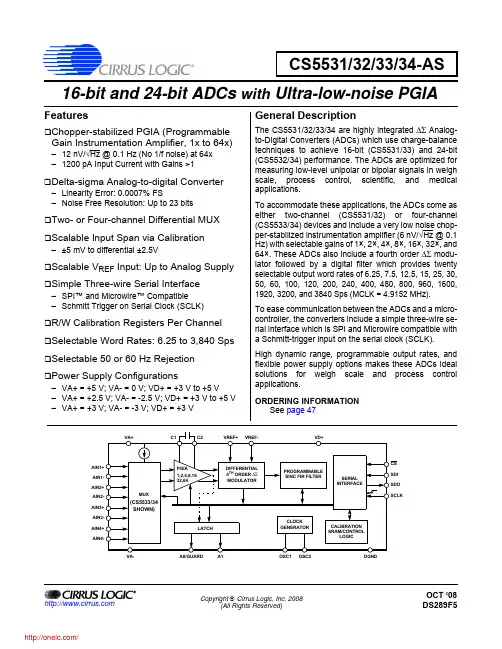
16-bit and 24-bit ADCs with Ultra-low-noise PGIAFeaturesChopper-stabilized PGIA (Programmable Gain Instrumentation Amplifier, 1x to 64x)–12 nV/√Hz @ 0.1 Hz (No 1/f noise) at 64x–1200pA Input Current with Gains >1Delta-sigma Analog-to-digital Converter–Linearity Error: 0.0007% FS–Noise Free Resolution: Up to 23 bitsTwo- or Four-channel Differential MUXScalable Input Span via Calibration –±5 mV to differential ±2.5VScalable VREF Input: Up to Analog SupplySimple Three-wire Serial Interface–SPI™ and Microwire™ Compatible–Schmitt Trigger on Serial Clock (SCLK)R/W Calibration Registers Per ChannelSelectable Word Rates: 6.25 to 3,840 SpsSelectable 50 or 60 Hz RejectionPower Supply Configurations–VA+ = +5 V; VA- = 0 V; VD+ = +3 V to +5 V–VA+ = +2.5 V; VA- = -2.5 V; VD+ = +3 V to +5 V–VA+ = +3 V; VA- = -3 V; VD+ = +3 VGeneral DescriptionThe CS5531/32/33/34 are highly integrated ∆Σ Analog-to-Digital Converters (ADCs) which use charge-balancetechniques to achieve 16-bit (CS5531/33) and 24-bit(CS5532/34) performance. The ADCs are optimized formeasuring low-level unipolar or bipolar signals in weighscale, process control, scientific, and medicalapplications.To accommodate these applications, the ADCs come aseither two-channel (CS5531/32) or four-channel(CS5533/34) devices and include a very low noise chop-per-stabilized instrumentation amplifier (6 nV/√Hz @ 0.1Hz) with selectable gains of 1×, 2×, 4×, 8×, 16×, 32×, and64×. These ADCs also include a fourth order ∆Σ modu-lator followed by a digital filter which provides twentyselectable output word rates of 6.25, 7.5, 12.5, 15, 25, 30,50, 60, 100, 120, 200, 240, 400, 480, 800, 960, 1600,1920, 3200, and 3840 Sps (MCLK=4.9152MHz).To ease communication between the ADCs and a micro-controller, the converters include a simple three-wire se-rial interface which is SPI and Microwire compatible witha Schmitt-trigger input on the serial clock (SCLK).High dynamic range, programmable output rates, andflexible power supply options makes these ADCs idealsolutions for weigh scale and process controlapplications.ORDERING INFORMATIONSee page47

9-1
24C1601 BLOCKCAT24C321/322(32K), CAT24C641/642(64K)
Supervisory Circuits with I2C Serial CMOS E2PROM, Precision Reset Controller and Watchdog Timer
DESCRIPTION
The CAT24CXXX is a single chip solution to threepopular functions of EEPROM memory, precision resetcontroller and watchdog timer. The 24C321/322(32K)and 24C641/642(64K) feature a I2C Serial CMOSEEPROM. Catalyst's advanced CMOS technology sub-stantially reduces device power requirements. The24CXXX features a 32-byte page and is available in 8-pinDIP or 8-pin SOIC packages.The reset function of the 24CXXX protects the systemduring brown out and power up/down conditions. Duringsystem failure the watchdog timer feature protects themicrocontroller with a reset signal. 24CXXX featuresactive low reset on pin 2 and active high reset on pin 7.24C321/641 features watchdog timer on the SDA line.24C322/642 does not feature the watchdog timer func-tion.

6 系列紧凑型数字化仪模数转换器
LPD64 产品技术资料
1用数字说话输入通道
4 个 SMA 输入
每个 SMA 输入都支持模拟、频谱(使用 DDC)或同时支持两者每条通道的性能
采样率: 25 GS/s
带宽: DC ~ 8 GHz (选配)
垂直分辨率: 12 位 ADC
实时 2 GHz DDC (选配)
记录长度: 125 M 点 (标配), 250 M 点 (选配)同类最低的噪声
同类最高的 ENOB
同类最优秀的通道间隔离度
实时数字下变频器 (DDC)已获专利的时域和频域单独控制功能
高达 2 GHz 捕获带宽 (选配)
IQ 数据传送到 PC 进行分析 (选配)
频率相对于时间关系图、相位相对于时间关系图、幅度相对于时间关系图 (选配)杰出的低噪声、垂直分辨率和精度
全新 TEK061 前端 ASICs 实现了低输入噪声
噪声 @ 1mV/div: 54.8 uV @ 1 GHz
输入范围: 10mV ~ 10 V 满刻度
DC 增益精度: +/-1.0%, 在所有 >1 mV/div 的增益设置下有效位数(ENOB):8.2 位 @ 1 GHz7.6 位 @ 2.5 GHz7.25 位 @ 4 GHz6.8 位 @ 6 GHz6.5 位 @ 8 GHz远程通信和连接
以太网 10/100/1000 端口
USB 3.0 设备端口 (USBTMC),高达 800 Mb/s
LXI 1.5 认证 (VXI-11)
使用 e*Scope 简便地实现远程访问,只需在浏览器中输入仪器的 IP
地址。屡获大奖的用户界面
驱动程序: IVI-C, IVI-COM, LabVIEW
支持 VISA, MATLAB, Python, C/C++/C#, 套接字测量分析
36 种标准测量
抖动测量 (选配)
DDR 测量 (选配)
功率测量 (选配)操作系统
封闭 Linux 嵌入式操作系统 (标配)
安全和解密 (选项 6-SEC)密码保护所有用户可接入的端口

© 2007 Microchip Technology Inc.
DS21930B-page 124AA00/24LC00/24C00 24AA01/24LC01B24AA014/24LC01424C01C24AA02/24LC02B 24C02C24AA024/24LC024 24AA025/24LC02524AA04/24LC04B 24AA08/24LC08B24AA16/24LC16B 24AA32A/24LC32A24AA64/24LC64/24FC6424AA128/24LC128/24FC12824AA256/24LC256/24FC256 24AA512/24LC512/24FC512
Features:•128-bit through 512 Kbit devices•Single supply with operation down to 1.7V for 24AAXX devices•Low-power CMOS technology:
-
1
mA active current, typical-1μA standby current, typical (I-temp)•2-wire serial interface bus, I2C™ compatible•Schmitt Trigger inputs for noise suppression•Output slope control to eliminate ground bounce•100kHz (1.7V) and 400kHz (≥ 2.5V) compatibility•1 MHz for 24FCXX products•Self-timed write cycle (including auto-erase)•Page write buffer•Hardware write-protect available on most devices•Factory programming (QTP) available•ESD protection > 4,000V•1 million erase/write cycles•Data retention > 200 years•8-lead PDIP, SOIC, TSSOP and MSOP packages•5-lead SOT-23 package (most 1-16 Kbit devices)•8-lead 2x3mm and 5x6mm DFN packages available•Pb-free and RoHS compliant•Available for extended temperature ranges:-Industrial (I): -40°C to +85°C-Automotive (E): -40°C to +125°CDescription:The Microchip Technology Inc. 24CXX, 24LCXX,24AAXX and 24FCXX (24XX*) devices are a family of128-bit through 512 Kbit Electrically Erased PROMs.The devices are organized in blocks of x8-bit memorywith 2-wire serial interfaces. Low-voltage designpermits operation down to 1.7V (for 24AAXX devices),with standby and active currents of only 1 μA and 1mA, respectively. Devices 1 Kbit and larger have pagewrite capability. Parts having functional address linesallow connection of up to 8 devices on the same bus.The 24XX family is available in the standard 8-pinPDIP, surface mount SOIC, TSSOP and MSOP pack-ages. Most 128-bit through 16 Kbit devices are alsoavailable in the 5-lead SOT-23 package. DFNpackages (2x3mm or 5x6mm) are also available. Allpackages are Pb-free (Matte Tin) finish.