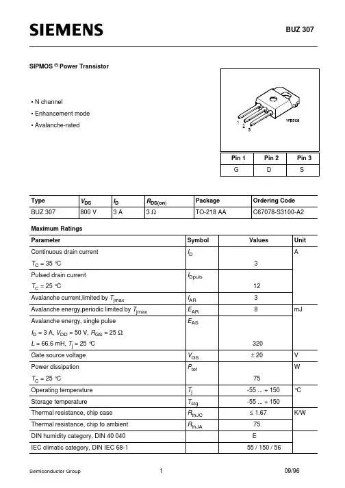
BUK9907-40ATC中文资料
- 格式:pdf
- 大小:355.30 KB
- 文档页数:15
BUK9907-40ATCTrenchPLUS logic level FETRev. 01 — 28 January 2002Product dataM3D7451.DescriptionN-channel enhancement mode field-effect power transistor in a plastic package using TrenchMOS™ technology, featuring very low on-state resistance and TrenchPLUS diodes for clamping, ElectroStatic Discharge (ESD) protection and temperature sensing.Product availability:BUK9907-40A TC in SOT263B.2.Featuress Typical on-state resistance 5.8m Ωs Q101 compliants ESD and overvoltage protectionsMonolithically integrated temperature sensor for overload protection.3.Applicationss Automotive and power switching:x 12V and 24V high power motor drives (e.g. Electrical Power Assisted Steering (EPAS))x Protected drive for lamps.4.Pinning informationTable 1:Pinning - SOT263B simplified outline and symbolPin Description Simplified outlineSymbol1gate (g)SOT263B2anode (a)3drain (d)4cathode (k)5source (s)mbmounting base;connected to drain (d)15mbMBL263MBL306das kg5.Quick reference dataTable 2:Quick reference dataSymbol Parameter Conditions Typ Max Unit V DSR(CL)drain-source clamping voltage T j=25°C; I GS(CL)=−2mA; I D=1A50-VI D drain current (DC)T mb=25°C; V GS=5V-140AP tot total power dissipation T mb=25°C-272WT j junction temperature-175°CR DSon drain-source on-state resistance T j=25°C;V GS=5V; I D=50A 5.87mΩT j=25°C;V GS=4.5V; I D=50A67.7mΩT j=25°C;V GS=10V; I D=50A 5.2 6.2mΩT j=25°C; I F=250µA658668mV V F temperature sense diode forwardvoltage−55°C<T j<175°C; I F=250µA−1.54−1.68mV/K S F temperature sense diode temperaturecoefficient6.Limiting values[1]Voltage is limited by clamping[2]Current is limited by power dissipation chip rating [3]Continuous current is limited by package.Table 3:Limiting valuesIn accordance with the Absolute Maximum Rating System (IEC 60134).Symbol ParameterConditionsMin Max Unit V DS drain-source voltage (DC)[1]-40V V DGS drain-gate voltage (DC) I DG =250µA[1]-40V V GS gate-source voltage (DC)[1]-±15V I Ddrain current (DC)T mb =25°C; V GS =5V;Figure 2and 3[2]-140A [3]-75A T mb =100°C; V GS =5V;Figure 2[3]-75A I DM drain current (peak value)T mb =25°C; pulsed; t p ≤10µs;Figure 3-560A P tot total power dissipation T mb =25°C;Figure 1-272W I DG(CL)drain-gate clamping current t p =5ms;δ=0.01-50mA I GS(CL)gate-source clamping currentcontinuous -10mA t p =5ms;δ=0.01-50mA V isol(FET -TSD)FET to temperature sense diodeisolation voltage -±100V T stg storage temperature−55+175°C T j operating junction temperature −55+175°C Source-drain diodeI DR reverse drain current (DC)T mb =25°C[2]-140A [3]-75A I DRM pulsed reverse drain currentT mb =25°C; pulsed; t p ≤10µs-560AClamping E DS(CL)Snon-repetitive drain-source clamping energyunclamped inductive load; I D =75A;V DS ≤40V; V GS =5V; R GS =10k Ω;starting T j =25°C- 1.4JElectrostatic Discharge V esdelectrostatic discharge voltage;pins 1,3,5Human Body Model; C =100pF;R =1.5k Ω-6kVV GS ≥5VFig 1.Normalized total power dissipation as a function of mounting base temperature.Fig 2.Continuous drain current as a function ofmounting base temperature.T mb =25°C; I DM single pulse.Fig 3.Safe operating area; continuous and peak drain currents as a function of drain-source voltage.03na190204060801001200255075100125150175200P der (%)T mb (ºC)03ne740255075100125150255075100125150175200T mb(o C)I D (A)Capped at 75 A due to packageP der P totP tot 25C °()-----------------------100%×=03ne75110102103 110102V DS (V)I D (A)DC100 ms10 ms R DSon = V DS /I D1 mst p = 10 µs100 µsCapped at 75 A due to package7.Thermal characteristics7.1Transient thermal impedanceTable 4:Thermal characteristics Symbol ParameterConditions Min Typ Max Unit R th(j-a)thermal resistance from junction to ambient vertical in still air --60K/W R th(j-mb)thermal resistance from junction to mounting baseFigure 4--0.55K/WFig 4.Transient thermal impedance from junction to mounting base as a function of pulse duration.03ne76Single Shot0.20.10.050.0210-310-210-11 10-610-510-410-310-210-1110t p (s)Z th(j-mb)(K/W)δ=0.5t pt p TPtTδ =8.CharacteristicsTable 5:CharacteristicsT j=25°C unless otherwise specifiedSymbol Parameter Conditions Min Typ Max Unit Static characteristicsV(BR)DG drain-gate zener breakdownvoltage I D=0.25mA; V GS=0V40--V T j=−55°C40--VV GS(th)gate-source threshold voltage I D=1mA; V DS=V GS;Figure91 1.52VT j=175°C0.5--VT j=−55°C−- 2.3V I DSS drain-source leakage current V DS=40V; V GS=0V-0.1100µAT j=175°C--250µAV(BR)GSS gate-source breakdownvoltage I G=±1mA;−55°C<T j<175°C1215-VI GSS gate-source leakage current V GS=±5V; V DS=0V-51000nAR DSon drain-source on-stateresistance V GS=5V; I D=50A;Figure7and8- 5.87mΩT j=175°C-−14mΩV GS=4.5V; I D=50A-67.7mΩV GS=10V; I D=50A- 5.2 6.2mΩV F temperature sense diodeforward voltageI F=250µA648658668mVS F temperature sense diodetemperature coefficient I F=250µA;−55°C<T j<175°C1.4 1.54 1.68mV/KV hys temperature sense diodeforward voltage hysteresis125µA<I F<250µA253250mV Dynamic characteristicsC iss input capacitance V GS=0V; V DS=25V;f=1MHz;Figure12-5836-pFC oss output capacitance-958-pF C rss reverse transfer capacitance-595-pFt d(on)turn-on delay time V DD=30V; R L=1.2Ω;V GS=5V; R G=1kΩ-3-µst r rise time-10-µs t d(off)turn-off delay time-17-µs t f fall time-11-µs L d internal drain inductance measured from upper edgeof drain mounting base tocentre of die- 2.5-nHL s internal source inductance measured from source leadto source bond pad-7.5-nHSource-drain diodeV SD source-drain (diode forward)voltageI S =25A; V GS =0V;Figure 19-0.85 1.2V t rr reverse recovery time I S =20A;dI S /dt =−100A/µs V GS =−10V; V DS =30V-85-ns Q rrecovered charge-250-nCTable 5:Characteristics …continued T j =25°C unless otherwise specified Symbol ParameterConditions Min Typ Max UnitT j =25°C; t p =300µs T j =25°C; I D =50AFig 5.Output characteristics: drain current as afunction of drain-source voltage;typical values.Fig 6.Drain-source on-state resistance as a functionof gate-source voltage; typical values.T j =25°C; t p =300µsFig 7.Drain-source on-state resistance as a functionof drain current; typical values.Fig 8.Normalized drain-source on-state resistance factor as a function of junction temperature.03ne770501001502002503003504000246810V DS (V)I D (A) 2.22.633.43.84.24.6V GS = 5 V6102.42.83.23.644.403ne790510152025246810V GS(V)R DSon (m Ω)03ne786810121416050100150200250300I D (A)R DSon (m Ω)V GS = 3 V3.23.43.63.8451003ne8900.511.52-6060120180T j (ºC)aa RDSon R DSon 25C °()----------------------------=I D =1mA; V DS =V GS T j =25°C; V DS =V GSFig 9.Gate-source threshold voltage as a function ofjunction temperature.Fig 10.Sub-threshold drain current as a function ofgate-source voltage.T j =25°C; V DS =25V V GS =0V; f =1MHzFig 11.Forward transconductance as a function ofdrain current; typical values.Fig 12.Input,output and reverse transfer capacitancesas a function of drain-source voltage; typical values.03na1700.511.522.5-60-202060100140180maxtypminV GS(th)T j (o C)(V)03na180.511.522.53maxtyp minI D V GS(V)10-610-510-410-310-210-1(A)03ne81020406080100120140020406080100I D(A)g fs (S)03ne86020004000600080001000012000140001600010-210-1110 102V DS (V)C (pF)C issC oss C rssV DS =25V T j =25°C; I D =50AFig 13.Transfer characteristics: drain current as afunction of gate-source voltage; typical values.Fig 14.Gate-source voltage as a function of turn-ongate charge; typical values.I DG(CL)=−2mA I D =10AFig 15.Drain-source clamping voltage as a function ofdrain current; typical values.Fig 16.Drain-source clamping voltage as a function ofgate current; typical values.03ne800204060801000.01.02.03.0V GS (V)I D (A)T j =175ºCT j =25ºC03ne87012345020406080100120Q G(nC)V GS (V)V DS = 14 VV DS = 35 V03ne8248.54949.55050.5510246810I D (A)V DSR(CL)(V)T j = 175 ºCT j = 25 ºCT j = -55 ºC03ne8340424446485052540123-I GS(CL) (mA)VDSR(CL) (V)T j = 175 ºCT j = 25 ºCT j = -55 ºCI F =250µA V F at T j =25°C; I F =250µAFig 17.Forward voltage of temperature sense diode asa function of junction temperature; typical values.Fig 18.Temperature coefficient of temperature sensediode as a function of forward voltage; typical values.V GS =0VFig 19.Reverse diode current as a function of reverse diode voltage; typical values.03ne84400500600700050100150200T j (ºC)V F (mV)03ne851.401.451.501.551.601.651.70645650655660665670675V F (mV)-S F (mV/K)maxmintyp03ne880204060801000.00.51.01.5V SD (V)I S (A)T j = 175 ºCT j = 25 ºC9.Package outlineFig 20.SOT263B.REFERENCESOUTLINE VERSION EUROPEAN PROJECTIONISSUE DATE IECJEDEC EIAJSOT263B5-lead TO-220DD 1q∅ pp 1L15L 1mounting baseL 2meQb0510 mmscalePlastic single-ended package; heatsink mounted; 1 mounting hole; 5-lead TO-220SOT263BDIMENSIONS (mm are the original dimensions)A E A 1cNotes1. Terminal dimensions are uncontrolled in this zone.2. Positional accuracy of the terminals is controlled in this zone.w MUNIT A 1D 1e p 1mm 1.7q Q A b D c L 2(2)0.54.34.1∅ p 3.83.6m 0.80.615.013.52.41.63.02.72.62.2w 0.40.70.415.815.20.850.704.54.11.391.276.45.910.39.7L 1(1)E L 01-01-1110.Revision historyTable 6:Revision historyRev Date CPCN Description0120020128-Product data; initial versionContact informationFor additional information, please visit .For sales office addresses, send e-mail to:sales.addresses@ .Fax: +31 40 27 2482511.Data sheet status[1]Please consult the most recently issued data sheet before initiating or completing a design.[2]The product status of the device(s) described in this data sheet may have changed since this data sheet was published. The latest information is available on the Internet at URL .12.DefinitionsShort-form specification —The data in a short-form specification is extracted from a full data sheet with the same type number and title. For detailed information see the relevant data sheet or data handbook.Limiting values definition — Limiting values given are in accordance with the Absolute Maximum Rating System (IEC 60134). Stress above one or more of the limiting values may cause permanent damage to the device.These are stress ratings only and operation of the device at these or at any other conditions above those given in the Characteristics sections of the specification is not implied. Exposure to limiting values for extended periods may affect device reliability.Application information — Applications that are described herein for any of these products are for illustrative purposes only. Philips Semiconductors make no representation or warranty that such applications will be suitable for the specified use without further testing or modification.13.DisclaimersLife support —These products are not designed for use in life support appliances, devices, or systems where malfunction of these products can reasonably be expected to result in personal injury. Philips Semiconductors customers using or selling these products for use in such applications do so at their own risk and agree to fully indemnify Philips Semiconductors for any damages resulting from such application.Right to make changes —Philips Semiconductors reserves the right to make changes, without notice, in the products, including circuits, standard cells, and/or software, described or contained herein in order to improve design and/or performance. Philips Semiconductors assumes noresponsibility or liability for the use of any of these products, conveys no licence or title under any patent, copyright, or mask work right to theseproducts,and makes no representations or warranties that these products are free from patent,copyright,or mask work right infringement,unless otherwise specified.14.TrademarksTrenchMOS —is a trademark of Koninklijke Philips Electronics N.V .Data sheet status [1]Product status [2]DefinitionObjective data Development This data sheet contains data from the objective specification for product development.Philips Semiconductors reserves the right to change the specification in any manner without notice.Preliminary dataQualificationThis data sheet contains data from the preliminary specification. Supplementary data will be published at a later date. Philips Semiconductors reserves the right to change the specification without notice, in order to improve the design and supply the best possible product.Product data ProductionThis data sheet contains data from the product specification. Philips Semiconductors reserves the right to make changes at any time in order to improve the design, manufacturing and supply. Changes will be communicated according to the Customer Product/Process Change Notification (CPCN) procedure SNW-SQ-650A.© Koninklijke Philips Electronics N.V .2002.Printed in The NetherlandsAll rights are reserved.Reproduction in whole or in part is prohibited without the prior written consent of the copyright owner.The information presented in this document does not form part of any quotation or contract,is believed to be accurate and reliable and may be changed without notice.No Contents1Description. . . . . . . . . . . . . . . . . . . . . . . . . . . . . 12Features . . . . . . . . . . . . . . . . . . . . . . . . . . . . . . . 13Applications. . . . . . . . . . . . . . . . . . . . . . . . . . . . 14Pinning information. . . . . . . . . . . . . . . . . . . . . . 15Quick reference data . . . . . . . . . . . . . . . . . . . . . 26Limiting values. . . . . . . . . . . . . . . . . . . . . . . . . . 37Thermal characteristics. . . . . . . . . . . . . . . . . . . 57.1T ransient thermal impedance . . . . . . . . . . . . . . 58Characteristics. . . . . . . . . . . . . . . . . . . . . . . . . . 69Package outline . . . . . . . . . . . . . . . . . . . . . . . . 1210Revision history. . . . . . . . . . . . . . . . . . . . . . . . 1311Data sheet status. . . . . . . . . . . . . . . . . . . . . . . 1412Definitions . . . . . . . . . . . . . . . . . . . . . . . . . . . . 1413Disclaimers. . . . . . . . . . . . . . . . . . . . . . . . . . . . 1414Trademarks. . . . . . . . . . . . . . . . . . . . . . . . . . . . 14。