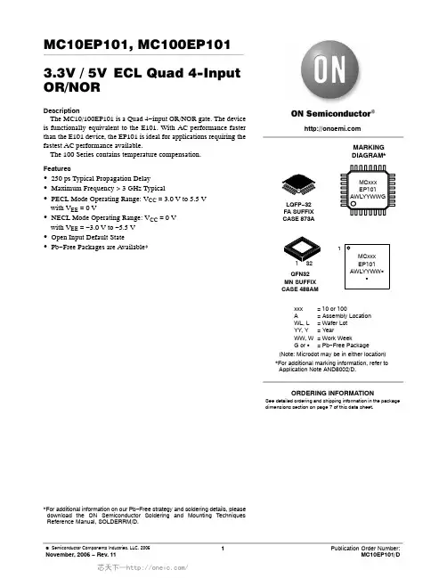
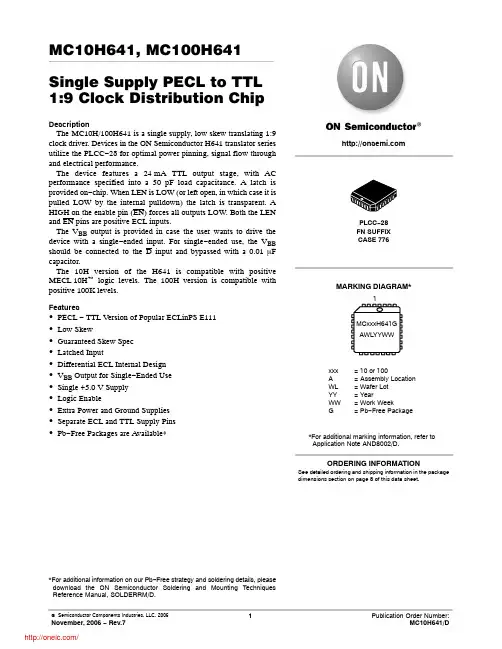
MC10H641, MC100H641 Single Supply PECL to TTL 1:9 Clock Distribution ChipDescriptionThe MC10H/100H641 is a single supply, low skew translating 1:9 clock driver. Devices in the ON Semiconductor H641 translator series utilize the PLCC−28 for optimal power pinning, signal flow through and electrical performance.The device features a 24 mA TTL output stage, with AC performance specified into a 50 pF load capacitance. A latch is provided on−chip. When LEN is LOW (or left open, in which case it is pulled LOW by the internal pulldown) the latch is transparent. A HIGH on the enable pin (EN) forces all outputs LOW. Both the LEN and EN pins are positive ECL inputs.The V BB output is provided in case the user wants to drive the device with a single−ended input. For single−ended use, the V BB should be connected to the D input and bypassed with a 0.01 m F capacitor.The 10H version of the H641 is compatible with positiveMECL 10H™ logic levels. The 100H version is compatible with positive 100K levels.Features•PECL − TTL Version of Popular ECLinPS E111•Low Skew•Guaranteed Skew Spec•Latched Input•Differential ECL Internal Design•V BB Output for Single−Ended Use•Single +5.0 V Supply•Logic Enable•Extra Power and Ground Supplies•Separate ECL and TTL Supply Pins•Pb−Free Packages are Available**For additional information on our Pb−Free strategy and soldering details, please download the ON Semiconductor Soldering and Mounting Techniques Reference Manual, SOLDERRM/D.MARKING DIAGRAM*xxx= 10 or 100A= Assembly LocationWL= Wafer LotYY= YearWW= Work WeekG=Pb−Free PackagePLCC−28FN SUFFIXCASE 776MCxxxH641GAWLYYWW1*For additional marking information, refer toApplication Note AND8002/D.See detailed ordering and shipping information in the package dimensions section on page 8 of this data sheet.ORDERING INFORMATIONV BB D D VE LEN GE EN1GT Q5VT Q4VT Q3GTGT Q6VT Q7VT Q8GT GTQ2VTQ1VTQ0GT5678910112524232221201926272823418171615141312Figure 1. Pinout: PLCC −28 (Top View)TTL OutputsQ0Q1Q2Q3Q4Q5Q6Q7Q8Figure 2. Logic DiagramTable 2. 10H PECL DC CHARACTERISTICSSymbol Characteristic Condition0°C25°C85°CUnit Min Max Min Max Min MaxI INH Input HIGH Current255175175m A I IL Input LOW Current0.50.50.5m A V IH Input HIGH Voltage V E = 5.0 V (Note 1) 3.83 4.16 3.87 4.19 3.94 4.28V V IL Input LOW Voltage V E = 5.0 V (Note 1) 3.05 3.52 3.05 3.52 3.05 3.55V V BB Output Reference Voltage V E = 5.0 V (Note 1) 3.62 3.73 3.65 3.75 3.69 3.81V NOTE:Device will meet the specifications after thermal equilibrium has been established when mounted in a test socket or printed circuit board with maintained transverse airflow greater than 500 lfpm. Electrical parameters are guaranteed only over the declared operating temperature range. Functional operation of the device exceeding these conditions is not implied. Device specification limit values are applied individually under normal operating conditions and not valid simultaneously.1.PECL V IH, V IL, and V BB are referenced to VE and will vary 1:1 with the power supply. The levels shown are for VE = 5.0 V.Table 3. 100H PECL DC CHARACTERISTICSSymbol Characteristic Condition0°C25°C85°CUnit Min Max Min Max Min MaxI INH Input HIGH Current255175175m A I INL Input LOW Current0.50.50.5m A V IH Input HIGH Voltage V E = 5.0 V (Note 2) 3.835 4.120 3.835 4.120 3.835 4.120V V IL Input LOW Voltage V E = 5.0 V (Note 2) 3.190 3.525 3.190 3.525 3.190 3.525V V BB Output Reference Voltage V E = 5.0 V (Note 2) 3.62 3.74 3.62 3.74 3.62 3.74V NOTE:Device will meet the specifications after thermal equilibrium has been established when mounted in a test socket or printed circuit board with maintained transverse airflow greater than 500 lfpm. Electrical parameters are guaranteed only over the declared operating temperature range. Functional operation of the device exceeding these conditions is not implied. Device specification limit values are applied individually under normal operating conditions and not valid simultaneously.2.PECL V IH, V IL, and V BB are referenced to VE and will vary 1:1 with the power supply. The levels shown are for VE = 5.0 V.Table 4. DC CHARACTERISTICS (V T = V E = 5.0 V ± 5%)Symbol CharacteristicT A = 0°C T A = + 25°C T A = + 85°CUnit Min Typ Max Min Typ Max Min Typ MaxI EE Power Supply CurrentPECL243024302430mA I CCH TTL243024302430mA I CCL273527352735mA NOTE:Device will meet the specifications after thermal equilibrium has been established when mounted in a test socket or printed circuit board with maintained transverse airflow greater than 500 lfpm. Electrical parameters are guaranteed only over the declared operating temperature range. Functional operation of the device exceeding these conditions is not implied. Device specification limit values are applied individually under normal operating conditions and not valid simultaneously.Table 5. TTL DC CHARACTERISTICS (V T = V E = 5.0 V ± 5%)Symbol0°C25°C85°C Characteristic Condition Min Max Min Max Min Max UnitV OH Output HIGH Voltage I OH = −15 mA 2.5 2.5 2.5V V OL Output LOW Voltage I OL = 24 mA0.50.50.5V I OS Output Short Circuit Current V OUT = 0 V−100−225−100−225−100−225mA NOTE:Device will meet the specifications after thermal equilibrium has been established when mounted in a test socket or printed circuit board with maintained transverse airflow greater than 500 lfpm. Electrical parameters are guaranteed only over the declared operating temperature range. Functional operation of the device exceeding these conditions is not implied. Device specification limit values are applied individually under normal operating conditions and not valid simultaneously.Table 6. AC CHARACTERISTICS (V T = V E = 5.0 V ± 5%)Characteristic T J = 0°C T J = + 25°C T J = + 85°CSymbol Condition Min Typ Max Min Typ Max Min Typ Max Unitt PLH t PHL Propagation DelayD to QCL = 50 pF (Note 3) 5.005.365.505.866.006.364.865.275.365.775.866.275.085.435.585.936.086.43nst skew Device SkewPart−to−PartSingle V CCOutput−to−Output CL = 50 pF (Note 4)CL = 50 pF (Note 5)CL = 50 pF (Note 6)100075035010007503501000750350pst PLH t PHL Propagation DelayLEN to QCL = 50 pF 4.9 6.9 4.9 6.9 5.07.0nst PLH t PHL Propagation DelayEN to QCL = 50 pF 5.07.0 4.9 6.9 5.07.0nst r t f Output Rise/Fall0.8 V to 2.0 VCL = 50 pF 1.71.61.71.61.71.6nsf MAX Max Input Frequency CL = 50 pF (Note 7)656565MHz t S Setup Time0.750.500.750.500.750.50ns t H Hold Time0.750.500.750.500.750.50ns NOTE:Device will meet the specifications after thermal equilibrium has been established when mounted in a test socket or printed circuit board with maintained transverse airflow greater than 500 lfpm. Electrical parameters are guaranteed only over the declared operating temperature range. Functional operation of the device exceeding these conditions is not implied. Device specification limit values are applied individually under normal operating conditions and not valid simultaneously.3.Propagation delay measurement guaranteed for junction temperatures. Measurements performed at 50 MHz input frequency.4.Skew window guaranteed for a single temperature across a V CC = V T = V E of 4.75 V to5.25 V (See Application Note in this data sheet).5.Skew window guaranteed for a single temperature and single V CC = V T = V E6.Output−to−output skew is specified for identical transitions through the device.7.Frequency at which output levels will meet a 0.8 V to 2.0 V minimum swing.Determining Skew for a Specific ApplicationThe H641 has been designed to meet the needs of very low skew clock distribution applications. In order to optimize the device for this application special considerations are necessary in the determining of the part−to−part skew specification limits. Older standard logic devices are specified with relatively slack limits so that the device can be guaranteed over a wide range of potential environmental conditions. This range of conditions represented all of the potential applications in which the device could be used. The result was a specification limit that in the vast majority of cases was extremely conservative and thus did not allow for an optimum system design. For non−critical skew designs this practice is acceptable, however as the clock speeds of systems increase overly conservative specification limits can kill a design.The following will discuss how users can use the information provided in this data sheet to tailor a part−to−part skew specification limit to their application. The skew determination process may appear somewhat tedious and time consuming, however if the utmost in performance is required this procedure is necessary. For applications which do not require this level of skew performance a generic part−to−part skew limit of 2.5 ns can be used. This limit is good for the entire ambient temperature range, the guaranteed V CC (V T, V E) range and the guaranteed operating frequency range.Temperature DependenceA unique characteristic of the H641 data sheet is that the AC parameters are specified for a junction temperature rather than the usual ambient temperature. Because very few designs will actually utilize the entire commercial temperature range of a device a tighter propagation delay window can be established given the smaller temperature range. Because the junction temperature and not the ambient temperature is what affects the performance of the device the parameter limits are specified for junction temperature. In addition the relationship between the ambient and junction temperature will vary depending on the frequency, load and board environment of the application. Since these factors are all under the control of the user it is impossible to provide specification limits for every possible application. Therefore a baseline specification was established for specific junction temperatures and the information that follows will allow these to be tailored to specific applications.Since the junction temperature of a device is difficult to measure directly, the first requirement is to be able to “translate” from ambient to junction temperatures. The standard method of doing this is to use the power dissipation of the device and the thermal resistance of the package. For a TTL output device the power dissipation will be a function of the load capacitance and the frequency of the output. The total power dissipation of a device can be described by the following equation:P D (watts) = I CC (no load) * V CC +V S* V CC * f * C L * # Outputswhere:V S= Output V oltage Swing = 3.0 Vf = Output FrequencyC L = Load CapacitanceI CC = I EE + I CCHFigure 1 plots the I CC versus Frequency of the H641 with no load capacitance on the output. Using this graph and the information specific to the application a user can determine the power dissipation of the H641.Figure 1. I CC versus f (No Load)01020304050607080FREQUENCY (MHz)NORMALIZEDICC12345Figure 2 illustrates the thermal resistance (in °C/W) for the PLCC−28 under various air flow conditions. By reading the thermal resistance from the graph and multiplying by the power dissipation calculated above the junction temperature increase above ambient of the device can be calculated.02004006008001000AIRFLOW (LFPM)THERMALRESISTANCE(3040506070C/W)°Figure 2. j JA versus Air FlowFinally taking this value for junction temperature and applying it to Figure 3 allows the user to determine thepropagation delay for the device in question. A more common use would be to establish an ambient temperature range for the H641’s in the system and utilize the above methodology to determine the potential increased skew of the distribution network. Note that for this information if the T PD versus Temperature curve were linear the calculations would not be required. If the curve were linear over all temperatures a simple temperature coefficient could be provided.Figure 3. T PD versus Junction Temperature−30JUNCTION TEMPERATURE (P R O P A G A T I O N D E L A Y (n s )5.2−101030507090110130°C)5.45.65.86.06.26.4V CC DependenceTTL and CMOS devices show a significant propagationdelay dependence with V CC . Therefore the V CC variation in a system will have a direct impact on the total skew of the clock distribution network. When calculating the skew between two devices on a single board it is very likely an assumption of identical V CC ’s can be made. In this case the number provided in the data sheet for part −to −part skew would be overly conservative. By using Figure 4 the skew given in the data sheet can be reduced to represent a smaller or zero variation in V CC . The delay variation due to the specified V CC variation is ≈ 270 ps. Therefore, the 1 ns window on the data sheet can be reduced by 270 ps if the devices in question will always experience the same V CC .The distribution of the propagation delay ranges given in the data sheet is actually a composite of three distributions whose means are separated by the fixed difference inpropagation delay at the typical, minimum and maximum V CC .Figure 4. D T PD versus V CC4.75VCC (V)T −1404.85 4.955.05 5.15 5.25−100−60−202060100140ΔP D (p s )Capacitive Load DependenceAs with V CC the propagation delay of a TTL output is intimately tied to variation in the load capacitance. The skew specifications given in the data sheet, of course, assume equal loading on all of the outputs. However situations could arise where this is an impossibility and it may be necessary to estimate the skew added by asymmetric loading. In addition the propagation delay numbers are provided only for 50 pF loads, thus necessitating a method of determining the propagation delay for alternative loads.Figure 5 shows the relationship between the two propagation delays with respect to the capacitive load on the output. Utilizing this graph and the 50 pF limits the specification of the H641 can be mapped into a spec for either a different value load or asymmetric loads.Figure 5. T PD versus LoadCAPACITIVE LOAD (pF)M O R M A L I Z E D P R O P A G A T I O N D E L A Y (n s )0.751020304050607080901000.800.850.900.951.001.051.101.15Rise/Fall Skew DeterminationThe rise−to−fall skew is defined as simply the difference between the T PLH and the T PHL propagation delays. This skew for the H641 is dependent on the V CC applied to the device. Notice from Figure 4 the opposite relationship of T PD versus V CC between T PLH and T PHL. Because of this the rise−to−fall skew will vary depending on V CC. Since in all likelihood it will be impossible to establish the exact value for V CC, the expected variation range for V CC should be used. If this variation will be the ± 5% shown in the data sheet the rise−to−fall skew could be established by simply subtracting the fastest T PLH from the slowest T PHL; this exercise yields 1.41 ns. If a tighter V CC range can be realized Figure 4 can be used to establish the rise−to−fall skew. Specification Limit Determination ExampleThe situation pictured in Figure 6 will be analyzed as an example. The central clock is distributed to two different cards; on one card a single H641 is used to distribute the clock while on the second card two H641’s are required to supply the needed clocks. The data sheet as well as the graphical information of this section will be used to calculate the skew between H641a and H641b as well as the skew between all three of the devices. Only the T PLH will be analyzed, the T PHL numbers can be found using the same technique. The following assumptions will be used:−All outputs will be loaded with 50 pF−All outputs will toggle at 30 MHz−The V CC variation between the two boards is ± 3 %−The temperature variation between the threedevices is ± 15°C around an ambient of 45°C.−500 lfpm air flowThe first task is to calculate the junction temperature for the devices under these conditions. Using the power equation yields:P D=I CC (no load) * V CC +V CC * V S * f * C L * # outputs=4.3 * 48m A * 5.0 V + 5.0 V * 3.0 V * 30 MHz *50 pF * 9=432 mW + 203 mW = 635 mWUsing the thermal resistance graph of Figure 2 yields a thermal resistance of 41°C/W which yields a junction temperature of 71°C with a range of 56°C to 86°C. Using the T PD versus Temperature curve of Figure 3 yields a propagation delay of 5.42 ns and a variation of 0.19 ns. Since the design will not experience the full ± 5% V CC variation of the data sheet the 1.0 ns window provided will be unnecessarily conservative. Using the curve of Figure 4 shows a delay variation due to a ± 3% V CC variation of ± 0.075 ns. Therefore the 1.0 ns window can be reduced to 1.0 ns − (0.27 ns − 0.15 ns) = 0.88 ns. Since H641a and H641b are on the same board we will assume that they will always be at the same V CC; therefore the propagation delay window will only be 1 ns − 0.27 ns = 0.73 ns.Putting all of this information together leads to a skew between all devices of0.19 ns + 0.88 ns(temperature + supply, and inherent device),while the skew between devices A and B will be only 0.19 ns + 0.73 ns(temperature + inherent device only).In both cases, the propagation delays will be centered around 5.42 ns, resulting in the following t PLH windows: T PLH = 4.92 ns − 5.99 ns; 1.07 ns window(all devices)T PLH= 5.00 ns − 5.92 ns; 0.92 ns window(devices a & b)Of course the output−to−output skew will be as shown in the data sheet since all outputs are equally loaded.This process may seem cumbersome, however the delay windows, and thus skew, obtained are significantly better than the conservative worst case limits provided at the beginning of this note. For very high performance designs, this extra information and effort can mean the difference between going ahead with prototypes or spending valuableFigure 6. Example ApplicationORDERING INFORMATIONDevice Package Shipping†MC10H641FN PLCC−2837 Units / Rail37 Units / RailMC10H641FNG PLCC−28(Pb−Free)MC10H641FNR2PLCC−28500 / Tape & Reel500 / Tape & ReelMC10H641FNR2G PLCC−28(Pb−Free)MC100H641FN PLCC−2837 Units / Rail37 Units / RailMC100H641FNG PLCC−28(Pb−Free)MC100H641FNR2PLCC−28500 / Tape & Reel500 / Tape & ReelMC100H641FNR2G PLCC−28(Pb−Free)†For information on tape and reel specifications, including part orientation and tape sizes, please refer to our Tape and Reel Packaging Specifications Brochure, BRD8011/D.Resource Reference of Application NotesAN1405/D−ECL Clock Distribution TechniquesAN1406/D−Designing with PECL (ECL at +5.0 V)AN1503/D−ECLinPS t I/O SPiCE Modeling KitAN1504/D−Metastability and the ECLinPS FamilyAN1568/D−Interfacing Between LVDS and ECLAN1672/D−The ECL Translator GuideAND8001/D−Odd Number Counters DesignAND8002/D−Marking and Date CodesAND8020/D−Termination of ECL Logic DevicesAND8066/D−Interfacing with ECLinPSAND8090/D−AC Characteristics of ECL DevicesPACKAGE DIMENSIONSPLCC −28FN SUFFIXPLASTIC PLCC PACKAGECASE 776−02ISSUE ESL−M S 0.010 (0.250) NST VIEW SNOTES:1.DATUMS −L−, −M−, AND −N− DETERMINED WHERE TOP OF LEAD SHOULDER EXITS PLASTIC BODY AT MOLD PARTING LINE.2.DIMENSION G1, TRUE POSITION TO BEMEASURED AT DATUM −T−, SEATING PLANE.3.DIMENSIONS R AND U DO NOT INCLUDE MOLD FLASH. ALLOWABLE MOLD FLASH IS 0.010 (0.250) PER SIDE.4.DIMENSIONING AND TOLERANCING PER ANSI Y14.5M, 1982.5.CONTROLLING DIMENSION: INCH.6.THE PACKAGE TOP MAY BE SMALLER THAN THE PACKAGE BOTTOM BY UP TO 0.012(0.300). DIMENSIONS R AND U ARE DETERMINED AT THE OUTERMOST EXTREMES OF THE PLASTIC BODY EXCLUSIVE OF MOLD FLASH, TIE BAR BURRS, GATE BURRS AND INTERLEAD FLASH, BUT INCLUDING ANY MISMATCH BETWEEN THE TOP AND BOTTOM OF THE PLASTIC BODY.7.DIMENSION H DOES NOT INCLUDE DAMBAR PROTRUSION OR INTRUSION. THE DAMBAR PROTRUSION(S) SHALL NOT CAUSE THE H DIMENSION TO BE GREATER THAN 0.037(0.940). THE DAMBAR INTRUSION(S) SHALL NOT CAUSE THE H DIMENSION TO BE SMALLER THAN 0.025 (0.635).DIM MIN MAX MIN MAX MILLIMETERSINCHES A 0.4850.49512.3212.57B 0.4850.49512.3212.57C 0.1650.180 4.20 4.57E 0.0900.110 2.29 2.79F 0.0130.0190.330.48G 0.050 BSC 1.27 BSC H 0.0260.0320.660.81J 0.020−−−0.51−−−K 0.025−−−0.64−−−R 0.4500.45611.4311.58U 0.4500.45611.4311.58V 0.0420.048 1.07 1.21W 0.0420.048 1.07 1.21X 0.0420.056 1.07 1.42Y −−−0.020−−−0.50Z 2 10 2 10 G10.4100.43010.4210.92K10.040−−− 1.02−−−____ON Semiconductor and are registered trademarks of Semiconductor Components Industries, LLC (SCILLC). SCILLC reserves the right to make changes without further notice to any products herein. SCILLC makes no warranty, representation or guarantee regarding the suitability of its products for any particular purpose, nor does SCILLC assume any liability arising out of the application or use of any product or circuit, and specifically disclaims any and all liability, including without limitation special, consequential or incidental damages.“Typical” parameters which may be provided in SCILLC data sheets and/or specifications can and do vary in different applications and actual performance may vary over time. All operating parameters, including “Typicals” must be validated for each customer application by customer’s technical experts. SCILLC does not convey any license under its patent rights nor the rights of others. SCILLC products are not designed, intended, or authorized for use as components in systems intended for surgical implant into the body, or other applications intended to support or sustain life, or for any other application in which the failure of the SCILLC product could create a situation where personal injury or death may occur. Should Buyer purchase or use SCILLC products for any such unintended or unauthorized application, Buyer shall indemnify and hold SCILLC and its officers, employees, subsidiaries, affiliates,and distributors harmless against all claims, costs, damages, and expenses, and reasonable attorney fees arising out of, directly or indirectly, any claim of personal injury or death associated with such unintended or unauthorized use, even if such claim alleges that SCILLC was negligent regarding the design or manufacture of the part. SCILLC is an Equal Opportunity/Affirmative Action Employer. This literature is subject to all applicable copyright laws and is not for resale in any manner.PUBLICATION ORDERING INFORMATIONECLinPS is a trademark of Semiconductor Components Industries, LLC (SCILLC).MECL 10H is a trademark of Motorola, Inc.分销商库存信息:ONSEMIMC10H641FNR2G MC10H641FNG MC10H641FNR2 MC100H641FN MC100H641FNG MC100H641FNR2 MC100H641FNR2G MC10H641FN。