HP8920A无线电综合测试仪说明书 (1)
- 格式:pdf
- 大小:149.55 KB
- 文档页数:8
HP8920A综合测试仪使用说明HP8920A/B综合测试仪使用方法一、测试线的连接MAX PWR 60W——仪器射频信号输入输出(注意观察标注的最大功率值,可能有些仪器只能测试5W或者10W的功率)。
接被测试机器的天线头。
(此处不能接错!200mw的那个头不要输入大功率,否则,会损坏仪器!)AUDIO IN (HI)——音频信号输入(接对讲机外接耳机插孔,输入信号后仪器显示相应指标)。
AUDIO OUT——音频信号输出(接对讲机外接话咪插孔,仪器里面模拟出来的音频信号经过话咪插孔进入到对讲机里面进行调制,然后通过仪器显示相关指标)。
其它部分按钮说明:VOLUME:调节仪器蜂鸣器声音大小。
SQUELCH:旋钮上的色点一般调节在中心位置合适,不然,有噪声。
二、测试1、发射测试(检测机器时,一般先测发射,因为发射部分的一些指标不良,会影响到接收):按仪器面板上的“TX”按键,进入发射指标检测界面。
连接好对讲机各测试线并打开电源,按下对讲机的PTT按键,发射时,主要看仪器屏幕上的三个指标:Tx Frequency :频率误差(实际发射出来的频率值和该信道标称频率的差值,一般±500Hz即可。
Tx Power:功率大小FM Deviation:最大频偏(一般在4KHz左右,加亚音频之后,会高0.7KHz。
该指标影响对讲机的送话)。
在发射状态下,把仪器的滤波器调小:即把“Filter 1”选择到“<20Hz”,再把“Filter 2”选择到“300Hz”,即可以在“FM Deviation”这一栏直接查看到该信道所加的模拟亚音频数值。
2、接收测试:按仪器面板上的“RX”按键,在该界面,要设置以下参数:转动面板上的那个大的旋钮,让光标停留在“RF Gen Freq”处,直接按数字键和单位按键,即输入要测试对讲机的接收频率(如458.825MHz),然后,再把光标移到“Amplitude”这一项,分别输入1mv和0.25uv两种场强参数(看你自己的习惯,也可以用“-DBm”的单位),以检测机器的失真度和灵敏度。
安捷伦8960实用简易操作说明安捷仑8960综合测试仪是GSM和CDMA手机测试常见的测试仪器,现把在生产过程常用的设置和调试在此说明,以便大家需要时参考1.如何将自动测试转换到手动测试?答:按面板右上方LOCAL键,进入本地设置状态即可(注:自动测试是指当仪器连接了电脑所有测试过程由电脑软件控制;手动测试即人工手动直接对仪器进行选择设置和测试。
)2.如何查看8960仪器的当前GPIB地址?答:1.按SYSTEM CONFIG键,进入系统设置界面,即可看到GPIB 地址,如:GPIB Address:20 3. 如何知道8960仪器当前的测试类型CDMA还是GSM?如何转换?答:1.按SYSTEM CONFIG键,进入系统设置界面,即可看到,如:Application:GSM/GPRS Mobile Test目前产线常用的有两种,(1)G网手机,采用GSM/GPRS Mobile Test(2)C网手机,采用CDMA2000 Mobile TestGSM手机校准时需把C网换成G网,否则不能校准,转换方法如下:先按按面板右上方LOCAL键,再Application Selection进入子画面,按Application Switch ,进入测试类型选项,通过旋钮选择GSM/GPRS Mobile Test或CDMA2000 Mobile Test,按下旋钮键确定,再选择YES 按下旋钮键确定,仪器将执行自动重启进入选定测试类项。
4.如何修改8960仪器的线损值?答:按SYSTEM CONFIG键,进入系统设置界面,按RF IN/OUT Amptd offset进入子画面,按IN/OUT Amptd offset setup,旋钮选择对应频段,按下旋钮键,进入线损值修改,如-10 dB。
(线损值理论上应该通过测试来定,但实际应用中直接输入经验值有8,10,12dB,使OK手机测试功率在33±3dB之内即可.5.如何用8960测试手机发射功率?答:在待机界面,按Mesutement Selection 进入弹出窗口,用旋钮选择功率***POWER 项,注意:GSM900M频段测试功率等级有5——15级, GSM1800M频段测试功率等级有0—15级,GSM900测试信道:1—124(中间信道62);GSM1800测试信道: 512—885(中间信道698),通话测试时:900M功率等级选最大5,信道选62,功率标准为33±3dB;1800M功率等级选最大0,信道选698,功率标准为33±3dB6.GSM手机接收灵敏度测试用手机建立一个呼叫连接,按下Measurement selection键(测试项目选择),选择测量项GSM Bit Error(误码),按下F7(BCH),再按F7调节Cell Power(信元功率),当Bit Error(误码)不超过2.4%时,Cell Power的值即为所测手机的接收灵敏度,国标为-102 dBm。

Keysight M8920A PXIe Radio Test Set 100 kHz to 3.8/6 GHzField radios are a vital lifeline for warfighters, firefighters andpeacekeepers. That’s why the new Keysight M8920A is designed to deliver the excellence you expect from your radio. All along your lifecycle, we open up capabilities that ranges from deep analysis in design to fast testing in production.Table of ContentsAccelerate MilCom and public safety radio manufacturing (3)Applications (3)Technical Specifications (4)Definitions and conditions (4)RF Analyzer Technical Specifications and Characteristics (5)RF Analyzer Technical Specifications and Characteristics (Continued) (6)RF Generator Technical Specifications and Characteristics (7)RF Generator Technical Specifications and Characteristics (Continued) (8)Audio Module Technical Specifications and Characteristics (8)Audio Module RX Audio Filters (9)Radio Test Application Specifications (9)N9093EM0E basic analog demodulation measurement application key specifications (9)N9093EM1E basic digital demodulation measurement application key specifications (9)Connectivity Test Application Specifications (10)WLAN 802.11ac (10)LTE-FDD/TDD (10)Bluetooth (10)Front Panel M9470A RF Interface Module Connections (10)General Specifications (11)Related Literature (12)Additional Information (12)Accelerate MilCom and public safety radio manufacturingDigital 2-way radios being developed for MilCom and the public safety radio market bring new testing challenges and hurdles to overcome for manufacturers and depot testing. Radio technologies are requiring wider bandwidths, higher frequencies, and multiple radio format capabilities.Product descriptionKeysight’s M8920A PXIe Radio Test Set supports many formats by combining PXI hardware with application-specific software in a single flexible and scalable chassis, providing broad multi-format coverage for next-generation radio testing.With Keysight’s new Radio Test Measurement Application (N9093), you can access and control multiple instruments on one screen while viewing a variety of critical measurements at the same time. Keysight can help deliver the operational excellence you expect from your radio.Applications−Cover all necessary analog AM and FM modulation test requirements.−Test APCO P1/P2, TETRA1, DMR, dPMR, ARIB, and custom modulation formats.−Test commercial connectivity formats including WLAN, LTE, Bluetooth®, etc.−All measurements can be performed with one click of a button.−Test analog Avionics Radios, and your Avionics Databus with optional Databus modulesM8920A PXIe Radio Test SetTechnical SpecificationsDefinitions and conditionsSpecifications describe the warranted performance of calibrated instruments. Data represented in this document are specifications under the following conditions unless otherwise noted.−Specifications are valid from 40° to 65 °C for individual module temperature, as reported by the module, and 20° to 35 °C for environment temperature unless otherwise noted −Calibrated instrument has been stored for a minimum of 2 hours within the allowed operating range−If instrument has previously been stored at a temperature range inside the allowed storage range, but outside the allowed operating range, instrument must have been stored for a minimum of 2hours within the allowed operating range before turn-on−30-minute warm-up time−Calibration cycle maintained−The RF, IF, and Source Alignments have been run within the previous 7 days−An ALL Alignment has been run within the previous 8 hours−If the temperature has changed more than 5 °C from the previous ALL AlignmentTypical describes additional product performance information that is not covered by the product warranty. It is performance beyond specifications that 80% of the units exhibit with a 95% confidence level. This data, shown in italics, does not include measurement uncertainty, and is valid only at room temperature (approximately 25 °C) after alignment within the stated alignment time and temperature limits.Nominal values indicate expected performance or describe product performance that is useful in the application of the product but are not covered by the product warranty.Recommended best practices in use−Use slot blockers and EMC filler panels in empty module slots to ensure proper operating temperatures. Keysight chassis and slot blockers optimize module temperature performance and reliability of test.−Set chassis fan to high at environmental temperatures above 45 °C.RF Analyzer Technical Specifications and Characteristics1.Instantaneous b andwidth (1 d B b andwidth) a vailable a round a c enter frequency o ver w hich t he i nput s ignal c an b e d igitized f or further a nalysis o rprocessing in the time, frequency or modulation domain.2.Calibration a ccuracy d epends o n h ow a ccurately t he f requency s tandard w as a djusted t o 10 M Hz. I f t he a djustment p rocedure i s f ollowed, t he c alibration accuracyis given by the specification. Achievable Initial Calibration Accuracy.3.The 3-dB cutoff frequency can be selected for the User-defined audio filters.RF Analyzer Technical Specifications and Characteristics (Continued)1.T/R port high power attenuation OFF2.Except at 100 MHz, 5 GHz, and 5.5 GHzRF Generator Technical Specifications and Characteristics1.Calibration a ccuracy d epends o n h ow a ccurately t he f requency s tandard w as a djusted t o 10 M Hz. I f t he a djustment p rocedure i s f ollowed, t he c alibrationa ccuracy is given by the specification. Achievable Initial Calibration Accuracy.2. Specifications apply when input port is set to Antenna InRF Generator Technical Specifications and Characteristics (Continued)Audio Module Technical Specifications and CharacteristicsAudio Module RX Audio FiltersRadio Test Application SpecificationsN9093EM0E basic analog demodulation measurement application key specificationsN9093EM1E basic digital demodulation measurement application key specifications1. The 3 dB cutoff frequency can be selected for the User-defined audio filters.Connectivity Test Application SpecificationsWLAN 802.11acLTE-FDD/TDDBluetoothFront Panel M9470A RF Interface Module ConnectionsGeneral SpecificationsFind us at Page 11PPFind us at Page 12Learn more at: For more information on Keysight Technologies’ products, applications or services , please contact your local Keysight office. The complete list is available at: /find/contactusThis information is subject to change without notice. © Keysight Technologies, 2018, Published in USA, Month July 11, 2019, 5992-2802ENRelated LiteratureFor more detailed product and specification information refer to the following literature and web pages: Publication titlePublication number M8920A PXIe Radio Test Set Technical Overview 5992-2821EN M8920A PXIe Radio Test Set Configuration Guide 5992-2800EN M8920A PXIe Radio Test Set Getting Started Guide M8920-90001 M9470A PXIe 50W Interface Module Data Sheet 5992-3140EN M9421A VXT PXIe Vector Transceiver Data Sheet 5992-1646EN M9260A PXIe Audio Analyzer Data Sheet 5992-1918EN PXIe Chassis Spec GuideM9019-90015 PC Tested Configurations with PXIe Chassis Technical Overview 5990-7632EN M9037A PXIe Embedded Controller Spec Guide M9037-90015 Interface Modules and Adapters for PXIe Systems5992-0377EN M924XA InfiniiVision PXIe Modular Oscilloscopes Data Sheet 5992-2003EN 6.5 Digit PXI Digital Multimeter Data Sheet 5992-2757EN PXIe Vector Network Analyzer Configuration Guide 5991-4885EN PXI Avionics Bus Interface Cards Configuration Guide 5992-2448EN 89600 VSA Software Configuration Guide5990-6386ENAdditional InformationProduct webpages:/find/M8920A /find/N9093 /find/PXIX-Series measurement applications: /find/X-Series_AppsSignal Studio Software:/find/signalstudio89600 VSA Software:/find/89600Bluetooth and the Bluetooth logos are trademarks owned byBluetooth SIG, Inc., U.S.A. and licensed to Keysight Technologies, Inc。
FLUKE 8922A8920A, 8921A & 8922AAutorangingFluke's autoranging feature allows you to carry out your testing without having to change ranges manually. A range can be placed on HOLD or manually stepped up to a higher range. On HOLD, the meter will remain in a given range regardless of changes in input levels. On STEP UP, the meter will increase ranges step-by-step until the switch is released. Peaking/Dipping MeterIn addition to an accurate digital display, all Fluke Voltmeters in the 8920-Series feature an analog meter for peak and null voltage adjustments. The meter indicates O to 100 percent full scale in each range.Linear Analog OutputModels 8920A and 8922A are equipped with a rear panel output for driving X-Y or st d p chart recorders, delivering voltages proportional to the display count. A 2-volt level equals 2000 counts, a 1-volt level equals 1000 counts, etc. This feature is not available on Model 8921A. AccuracyFluke Digital Voltmeters avoid the possibilities for error so common in analog meters. The digital displays eliminate the likelihood of misreading the meter due to viewing angle problems of parallax common with analog meters. Also, the accuracy of 8920-Series Voltmeters is specified as a percent of reading rather than as percent of full scale.Percent of reading accuracy does not degrade for measurements at the low end of a scale. Front panel switching offers a choice of readings in dB or volts.Technical SpecificationsThe a ccuracy s pecifications b elow apply from 9% to 100% of full scale and from 18°C to 28°C for 90 days. For six-month specifications multiply figures by 1.5.AC Accuracy: ± % of voltage reading or ±dB (8920A/8921 A)Range 2Hz 10 H z 20Hz 50Hz 10 kHz 700V200V1%or 0.5%or 20V 0.15dB 0.1 dB 2V Not200mV Speci-5%orlied 0.5dB 2%or 1%or 20 m V 0.25 d B 0.15dB3%or 2%or 2mV0.35dB 0.25dBAC Accuracy: ± % of voltage reading or ±dB(8922A)Range 2Hz 10 H z 20Hz 50Hz 10 k HzFILTER IN I700V200V 1%or•0.15 d B 1%or 0.5%or20V 0.15 d B 0.1 d B2V 5%or200 mV 3%or• 0.5dB0.35dB2%or•0.25dB 2%or 1%or20 mV 0.25 d B 0.15 d B5%or0.5dB5%or• 5%or 3%or 2%or I2 mv0.5 d B .. 0.5dB 0.35 d B 0.25dB• Valid when AC + DC DAMPING is selected andinput has no de components.••Below 2 mV add number of digits (N) to ±5% voltage readings, where N = 5 + mV input. Or, for dBreadings. add N to ±0.5 dB, where N = 0.5 + (mVinput)2AC+DC Accuracy: Add to AC accuracy specifications (above) ±10 digits or ±0.5 dB above 2mV, or ±100 digits or ±5.0 dB below 2 mV. Forde only, add above digits to 50 Hz to 10 kHzspecificationsFunctions: True RMS measurements only. ACor AC+ DC (8920A and 8921 A); AC or AC+ DCwith damping (8922A)Maximum Input: 700V rms or 1 O OOV peak, not toexceed a volt-hertz product of 1 x 10⁸ on anyrangeMaximum Common Mode Voltage8920A and 8922A: 400 mV rms or 600 mVpeak8921A: 500V rms or 700V peakAC Common Mode Rejection: �60 dB at 50 and60 Hz with 1000 unbalanceDC Common Mode Rejection: �100 dB, 1000unbalanceCrest Factor: 7 at full scale, increasing downscale by 7 times the voltage range divided by thevoltage input. Degrades below 10 Hz, annunciated when capability exceeded (8922A only)Input Impedance: 10 MO shunted by <30 pF200kHz 1 MHz 2MHz 10 M Hz 20MHzNot Specified0.7%or0.15 d B3% o r0.35 d B 5%or0.5dB2%or0.25dB 4%or0.4dB I3%or0.35dB200kHz 1 MHz 2MHz 11 MHzFILTER OUTNot Specified0.7%or0.15 d B3%or0.35 d B2%or 5%or0.25 d B 0.5dB4% o r0.4 d BVoltage R11nges: 2 mV, 20 mV, 200 mV, 2V, 20V,200V, 700VRanging: Autoranging with HOLD to defeat a�to•ranging and STEP UP for manual ranging.Ranges up at 2000 counts and ranges down at180 countsDecibel Ranges: In the autorange mode, theinstrument appears as though it has a singlerange spanning 131 dBdBm Reference: Twelve user-selectable impedances are provided to reference a O dBm, 1mW level (500,750,930, 1100, 1240, 1350,1500, 3000, 6000, 9000, 10000, and 12000)(dBV = 10000)Relative dB Reference: A voltage input presentwhen this button is pushed is held as "O dB"reference point. Subsequent readings indicate±deviations from this pointVoltage Resolution: 0.05% of ranges (3½ digits)Decibel Resolution: O.Q1 dB (4½ digits)Typical-3 dB Points: 40 MHz on 20 mV thru 20Vranges and 4 MHz on 2 mV range (8920A/8921 A); 22 MHz on 2 mV to 20V ranges (8922A)Low Pass Filter: Approximately 200 kHz -3 dBpoint, on 8922A onlyReading Rate: 2.5/s or 1 /s with ac + de withdamping (8922A)Autorange Rate: <950 ms or <3.5s with ac + dewith damping (8922A)Response Time: (To rated accuracy) <1.6s or<7s with ac + de with damping (8922A)Readout: Panel-select able for volts or dB,auto•matic decimal point location: analog peaking/dipping meter. " V .. "V .. "dB,,LED Annunciators: Indicate m , ,"REL REF," and "2 MHz MAX" for 2 mV range(8920A and 8921A) and "UNCAL" when crestfactor limitation exceeded (8922A)Overrange: Flashes maximum reading for thatrangeUnderrange: Flashes decimalLinear Analog Output: (8920A and 8922A only)Linear output of 2000 mV de for a 2000-countreadout; ±1.0% relative to display; essentiallyoo output into a �10 kO load; non-isolated, withoutput common same as input common。
HP8920A/B综合测试仪使用方法一、测试线的连接MAX PWR 60W——仪器射频信号输入输出(注意观察标注的最大功率值,可能有些仪器只能测试5W或者10W的功率)。
接被测试机器的天线头。
(此处不能接错!200mw的那个头不要输入大功率,否则,会损坏仪器!)AUDIO IN (HI)——音频信号输入(接对讲机外接耳机插孔,输入信号后仪器显示相应指标)。
AUDIO OUT——音频信号输出(接对讲机外接话咪插孔,仪器里面模拟出来的音频信号经过话咪插孔进入到对讲机里面进行调制,然后通过仪器显示相关指标)。
其它部分按钮说明:VOLUME:调节仪器蜂鸣器声音大小。
SQUELCH:旋钮上的色点一般调节在中心位置合适,不然,有噪声。
二、测试1、发射测试(检测机器时,一般先测发射,因为发射部分的一些指标不良,会影响到接收):按仪器面板上的“TX”按键,进入发射指标检测界面。
连接好对讲机各测试线并打开电源,按下对讲机的PTT按键,发射时,主要看仪器屏幕上的三个指标:Tx Frequency :频率误差(实际发射出来的频率值和该信道标称频率的差值,一般±500Hz即可。
Tx Power:功率大小FM Deviation:最大频偏(一般在4KHz左右,加亚音频之后,会高0.7KHz。
该指标影响对讲机的送话)。
在发射状态下,把仪器的滤波器调小:即把“Filter 1”选择到“<20Hz”,再把“Filter 2”选择到“300Hz”,即可以在“FM Deviation”这一栏直接查看到该信道所加的模拟亚音频数值。
2、接收测试:按仪器面板上的“RX”按键,在该界面,要设置以下参数:转动面板上的那个大的旋钮,让光标停留在“RF Gen Freq”处,直接按数字键和单位按键,即输入要测试对讲机的接收频率(如458.825MHz),然后,再把光标移到“Amplitude”这一项,分别输入1mv和0.25uv两种场强参数(看你自己的习惯,也可以用“-DBm”的单位),以检测机器的失真度和灵敏度。
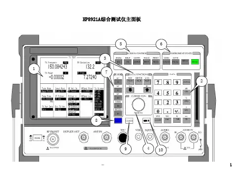

Agilent8920/8921通信测试仪(综测)使用说明一、仪器面板键盘操作及菜单1、面板CRT显示●RX TEST—接收机测试屏幕,可显示RF和AF控制及接收机测试结果。
●TX TEST—发射机测试屏幕,可显示RF和AF控制及发射机测试结果。
●DUPLEX TEST—双工测试屏幕,可同时显示RF和AF控制及收发信机测试结果。
●TESTS—访问来自存储卡、内部ROM/RAM及外接磁盘驱动器装入的程序,可对其编辑与自动运行的屏幕,显示测试结果。
●RF GENERATOR—射频信号源屏幕,用于显示射频与调制信号的控制及测试结果。
●RF ANAL YZER—射频分析仪屏幕,用于显示射频与解调信号的控制及测试结果。
●AF ANAL YZER—音频分析仪屏幕,用于显示音频信号的控制与测试结果。
●OSCILLOSCOPE—示波器屏幕,用于完成对示波器的控制及显示测量结果。
●SPECTRUM ANAL YZER—频谱分析仪屏幕。
●SIGNALING ENCODER—信令编码器屏幕。
●SIGNALING DECODER—信令解码器屏幕。
●RADIO INT—无线电接口与屏幕,显示仪器内置无线电接口卡对外接模块与设备的自动测试结果。
2、面板连接器与控制器●POWER—仪器的电源开关键。
●RF IN/OUT连接器—是一阻抗为50Ω的N型阴性插座,用作射频信号源的输出与调制分析仪的输入接口,允许连续输入60W,或输入100W功率。
●DUPLEX OUT连接器—是一阻抗为50Ω的BNC型阴性插座,用作射频信号源及跟踪信号源的输出端口。
●ANT IN连接器—用作小功率射频信号(≤200Mw)及空中信号的输入端口。
●MIC/ACC接口—是一8针DIN接口,可提供多种用途的连接:MIC IN—当KEY IN接地时去调制射频发生器(先滤波与放大);KEY IN—用于射频信号源的输出开/关状态控制,及在TX TEST与RX TEST屏幕之间的转换控制;KEY OUT1与KEY OUT2用于一部外设的开/关控制。
HP8920/8921使用说明一、主要功能1.信号发生器:HP8920/8921可以生成多种模拟和数字调制的信号,如AM、FM、带宽调制、群组编码、数字调幅等,可模拟各种通信系统所需的信号。
2.信号接收器:HP8920/8921能接收和分析各种调制信号,如FM、PM、AM、数字调制等,并提供实时功率、频谱和误码性能的测量结果。
3.频谱分析仪:HP8920/8921具备高精度频谱测量功能,可以测量多种信号的频率、偏移、谱纹、总谱和谱线等参数。
4.误码仪:HP8920/8921能提供误码性能的测量,包括误码率、误码秒数、比特误码率等指标。
5.对话功能:HP8920/8921可以进行双向对话,支持内置话筒和扬声器,方便进行通信测试。
二、使用方法1.设置信号源:使用菜单或快捷键设置HP8920/8921的信号源参数,包括频率、功率、调制方式等。
2.设置信号接收:使用菜单或快捷键设置HP8920/8921的接收参数,如频率范围、带宽、接收灵敏度等。
3.发射信号:在信号源菜单中选择信号类型和参数,并将发射天线与接收天线相连,发射信号。
4.接收信号:选择菜单中的接收模式,如FM、AM等,接收并分析信号。
5.频谱分析:选择频谱分析仪功能,输入待测信号,HP8920/8921将自动显示频谱和相关参数。
6.误码测量:选择误码仪功能,输入待测信号,HP8920/8921将自动统计并显示误码率和误码秒数。
7.对话测试:选择对话功能,进行双向通信测试,可以通过内置话筒和扬声器进行对话。
三、注意事项1.在进行测试前,请先根据测试要求设置相关参数,并连接好天线和输入输出设备。
2.执行项功能前,请确保已经选择了正确的模式,并根据提示操作。
3.在进行频谱测量时,需注意选择合适的分析带宽和显示方式,以获得准确的结果。
4.在进行误码测量时,确保输入信号质量和中断率,并选择合适的测量时长和统计方式。
四、如何获取更多信息1.参考用户手册:HP8920/8921配有详细的用户手册,其中包含了更多详细的功能和操作说明。
HP8920HP8921HP8924C综测详细操作一、射频分析RF ANALYZER模式------------------------2二、接收机测试模式------------------------4三、音频分析------------------------6四、发射机测试------------------------9五、射频信号发生器------------------------12六、双工模式------------------------14七、频谱分析------------------------17八、示波器------------------------22专业对讲机方案提供商联创电子赖工整理泉州市南安大霞美南丰花园城QQ:27116723一、射频分析RF ANALYZER模式本屏为射频分析RF ANALYZER模式。
用于测试发射机的各种发射参数。
说明如下:一、Tune Mode调谐模式。
可自动Auto和手动Manual。
a)当Tune Mode调谐模式设置为手动Manual时,Tx Frequency以误差形式显示,并显示为TX Freq Error。
b)当Tune Mode调谐模式设置为自动Auto时,Tx Frequency以频率显示。
二、Tune Freq调谐频率。
三、TX Power发射功率。
四、Input Port射频输入口选项。
a)RF In表示射频信号从射频输入/输出口RF IN/OUT进。
通常大功率信号从此口进。
b)Ant表示射频信号从天线输入口ANT IN进。
弱小信号一般从此口进。
五、Input Atten输入衰减。
可选自动Auto和保持Hold。
a)当选自动时,机器根据输入信号的大小,自动选择输入衰减值0dB,20dB或40dB。
b)当选择保持时,衰减值保持不变,可手动选择衰减值。
六、Sensitivity天线输入口ANT IN灵敏度选择。
a)Normal表示正常灵敏度。
Si8920 Data SheetIsolated Amplifier for Current Shunt MeasurementThe Si8920 is a galvanically isolated analog amplifier. The low-voltage differential input is ideal for measuring voltage across a current shunt resistor or for any place where a sensor must be isolated from the control system. The output is a differential analog sig-nal amplified by either 8.1x or 16.2x.The very low signal delay of the Si8920 allows control systems to respond quickly to fault conditions or changes in load. Low offset and gain drift ensure that accuracy is maintained over the entire operating temperature range. Exceptionally high common-mode transient immunity means that the Si8920 delivers accurate measurements even in the presence of high-power switching as is found in motor drive systems and inver-ters.The Si8920 isolated amplifier utilizes Silicon Labs’ proprietary isolation technology. It supports up to 5.0 kVrms withstand voltage per UL1577. This technology enables higher performance, reduced variation with temperature and age, tighter part-to-part matching, and longer lifetimes compared to other isolation technologies.Automotive Grade is available for certain part numbers. These products are built using automotive-specific flows at all steps in the manufacturing process to ensure the robust-ness and low defectivity required for automotive applications.KEY FEATURES•Low voltage differential input•±100 mV and ±200 mV options•Low signal delay: 0.75 µs•Input offset: 0.2 mV•Gain error: <0.5%•Excellent drift specifications•1 µV/°C offset drift•10 ppm/°C gain drift•Nonlinearity: 0.025% full-scale•Low noise: 0.10 mVrms over 100 kHz bandwidth•High common-mode transient immunity: 75 kV/µs•Compact packages•16-pin wide body SOIC•8-pin surface mount DIP•–40 to 125 °C•AEC-Q100•Automotive-grade OPNs available•AIAG compliant PPAP documentationsupport•IMDS and CAMDS listing supportIndustrial Applications•Industrial and renewable energy inver-ters•AC, Brushless, and DC motor controlsand drives•Variable speed motor control in consum-er white goods•Isolated switch mode and UPS powersuppliesSafety Regulatory Approvals•UL 1577 recognized•Up to 5000 Vrms for 1 minute •CSA component notice 5A approval •IEC 60950-1 (reinforced insulation)•VDE certification conformity•VDE0884 Part 10 (basic/reinforcedinsulation)•CQC certification approval•GB4943.1Automotive Applications •Hybrid and EV traction inverters •Onboard chargers•Charging pedestalsSi8920 Data SheetOrdering Guide 1. Ordering GuideTable 1.1. Ordering Guide for Valid OPNsAutomotive Grade OPNsAutomotive-grade devices are built using automotive-specific flows at all steps in the manufacturing process to ensure robustness and low defectivity. These devices are supported with AIAG-compliant Production Part Approval Process (PPAP) documentation, and fea-ture International Material Data System (IMDS) and China Automotive Material Data System (CAMDS) listing. Qualifications are compli-ant with AEC-Q100, and a zero-defect methodology is maintained throughout definition, design, evaluation, qualification, and mass pro-duction steps.Table 1.2. Ordering Guide for Automotive Grade OPNs1, 2, 4, 5Table of Contents1. Ordering Guide (2)2. System Overview (4)3. Current Sense Application (5)4. Electrical Specifications (6)4.1 Typical Operating Characteristics (11)4.2 Regulatory Information (13)5. Pin Descriptions (15)6. Packaging (16)6.1 Package Outline: DIP8 (16)6.2 Land Pattern: DIP8 (17)6.3 Package Outline: 16-Pin Wide Body SOIC (18)6.4 Land Pattern: 16-Pin Wide Body SOIC (20)6.5 Top Marking: DIP8 (21)6.6 Top Marking: 16-Pin Wide Body SOIC (22)7. Revision History (23)System Overview 2. System OverviewThe input to the Si8920 is designed for low-voltage, differential signals. This is ideal for connection to low resistance current shunt measurement resistors. The Si8920A has a full scale input range of ±100 mV, and the Si8920B has a full scale input range of ±200 mV. In both cases, the internal gain is set so that the full scale output is 1.6 V.The Si8920 modulates the analog signal in a unique way for transmission across the semiconductor based isolation barrier. The input signal is first converted to a pulse-width modulated digital signal. For transmission across the isolation barrier, the signal is further modulated with a high frequency carrier. On the other side of the isolation barrier, the signal is demodulated and the carrier portion is removed. The resulting PWM signal is then used to faithfully reproduce the analog signal. This solution provides exceptional signal bandwidth and accuracy.AONFigure 2.1. Functional Block Diagram3. Current Sense ApplicationIn the driver circuit presented below, the Si8920 is used to amplify the voltage across the sense resistor, RSENSE, and transmit the analog signal to the low-voltage domain across an isolation barrier. Isolation is needed because the voltage of RSENSE with respect to ground will swing between 0 V and the high voltage rail connected to the drain of Q1.To 3.3 to 5VLow Side Gate Driver Floating Gate Driver High Figure 3.1. Current Sense ApplicationThe load in this application can be a motor winding or a similar inductive winding. In a three-phase motor drive application, this circuit would be repeated three times, one for each phase. RSENSE should be a small resistor value to reduce power loss. However, an ex-cessively low resistance will reduce the signal-to-noise ratio of the measurement. Si8920 offers two specified full-scale input options,±100 mV (Si8920A) and ±200 mV (Si8920B), for optimizing the value of RSENSE.AIP and AIN connections to the RSENSE resistor should be made as close as possible to each end of the RSENSE resistor as trace resistance will add error to the measurement. The input to the Si8920 is differential, and the PCB traces back to the input pins should run in parallel. This ensures that any large noise transients that occur on the high-voltage side are coupled equally to the AIP and AIN pins and will be rejected by the Si8920 as a common-mode signal.The amplifier bandwidth of the Si8920 is approximately 950 kHz. If further input filtering is required, a passive, differential RC low-pass filter can be placed between RSENSE and the input pins. Values of R1 = R2 = 20 Ω and C1 = 10 nF, as shown in Figure 4.8 Step Response Low to High on page 11, provides a cutoff at approximately 400 kHz. For the lowest gain error, R1 and R2 should always be less than 33 Ω to keep the source impedance sufficiently low compared to the Si8920 input impedance.The common-mode voltage of AIN and AIP must be greater than –0.2 V but less than 1 V with respect to GNDA. To meet this require-ment, connect GNDA of the Si8920 to one side of the RSENSE resistor. In this example, GNDA, RSENSE, the source of Q1, and the drain of Q2 are connected. The ground of the gate driver (Silicon Labs’ Si8234 in this circuit) is also commonly connected to the same node.The Q1 gate driver has a floating supply, 24 V in this example. Since the input and output of the Si8920 are galvanically isolated from each other, separate power supplies are necessary on each side. Q3, R3, C3, and D1 make a regulator circuit for powering the input side of the Si8920 from this floating supply. D1 establishes a voltage of 5.6 V at the base of Q3. R3 is selected to provide a Zener current of 10 mA for D1. C3 provides filtering at the base of Q3, and the emitter output of Q3 provides approximately 5 V to VDDA. C2is a bypass capacitor for the supply and should be placed at the VDDA pin with its return trace connecting to the GNDA connection at RSENSE.C4, the local bypass capacitor for the B-side of Si8920, should be placed closed to VDDB supply pin with its return close to GNDB. The output signal at AOP and AON is differential with a nominal gain of 8.1 (Si8920B) or 16.2 (Si8920A) and common mode of 1.1 V. The outputs are sampled by a differential input ADC. Depending on the sample rate of the ADC, an anti-aliasing filter may be required. A simple anti-aliasing filter can be made from the passive components, R4, C6, and R5. The characteristics of this filter are dictated by the input topology and sampling frequency of the ADC. However, to ensure the Si8920 outputs are not overloaded, R4 = R5 > 5 kΩ and C6 can be calculated by the following equation:C 6=12×π×(R 4+R 5)×f 3dBCurrent Sense Application4. Electrical SpecificationsTable 4.1. Electrical Specifications V DDA, V DDB = 5 V, T A = –40 to +125 °C; typical specs at 25 °CSupplyFigure 4.1. Common-Mode Transient Immunity Characterization CircuitTable 4.2. IEC Safety Limiting Values1Table 4.3. Thermal CharacteristicsFigure 4.2. Thermal Derating Curve for Safety Limiting Current (DIP8)Figure 4.3. Thermal Derating Curve for Safety Limiting Current (WB SOIC-16)Table 4.4. Absolute Maximum Ratings14.1 Typical Operating CharacteristicsFigure 4.4. Amplifier Bandwidth Figure 4.5. Gain Error vs. TemperatureFigure 4.6. IDDB vs. Temperature Figure 4.7. IDDA vs. TemperatureFigure 4.8. Step Response Low to High Figure 4.9. Step Response High to LowFigure 4.10. CMRR vs. Frequency Figure 4.11. Normalized Differential Input Resistance vs. Tem-peratureFigure 4.12. Si8920A Typical V OUT vs. V IN Figure 4.13. Si8920B Typical V OUT vs. V IN4.2 Regulatory InformationTable 4.5. Regulatory Information1, 2CSAThe Si8920 is certified under CSA Component Acceptance Notice 5A. For more details, see File 232873.60950-1: Up to 600 V RMS reinforced insulation working voltage; up to 1000 V RMS basic insulation working voltage.VDEThe Si8920 is certified according to VDE 0884-10. For more details, see File 5006301-4880-0001.VDE 0884-10: Up to 1200 V peak for reinforced insulation working voltage.ULThe Si8920 is certified under UL1577 component recognition program. For more details, see File E257455.Rated up to 5000 V RMS isolation voltage for basic protection.CQCThe Si8920 is certified under GB4943.1-2011.Rated up to 600 V RMS reinforced insulation working voltage; up to 1000 V RMS basic insulation working voltage.Note:1.Regulatory Certifications apply to 5 kV RMS rated devices which are production tested to 6.0 kV RMS for 1 sec.2.Regulatory Certifications apply to3.75 kV RMS rated devices which are production tested to4.5 kV RMS for 1 sec.Table 4.6. Insulation and Safety-Related SpecificationsTable 4.7. IEC 60664-1 (VDE 0884) RatingsTable 4.8. VDE 0884-10 Insulation Characteristics15. Pin DescriptionsVDDA NC GNDAVDDBAIP NC NC GNDA AOP AON VDDA GNDA AOP AONAIP VDDB GNDBTable 5.1. Si8920 Pin DescriptionsPin Descriptions6. Packaging6.1 Package Outline: DIP8The figure below illustrates the package details for the Si8920 in a DIP8 package. The table lists the values for the dimensions shown in the illustration.Figure 6.1. DIP8 PackageTable 6.1. DIP8 Package Diagram Dimensions6.2 Land Pattern: DIP8The figure below illustrates the recommended land pattern details for the Si8920 in a DIP8 package. The table lists the values for the dimensions shown in the illustration.Figure 6.2. DIP8 Land PatternTable 6.2. DIP8 Land Pattern Dimensions16.3 Package Outline: 16-Pin Wide Body SOICThe figure below illustrates the package details for the Si8920 in a 16-Pin Wide Body SOIC package. The table lists the values for the dimensions shown in the illustration.Figure 6.3. 16-Pin Wide Body SOIC PackageTable 6.3. 16-Pin Wide Body SOIC Package Diagram Dimensions6.4 Land Pattern: 16-Pin Wide Body SOICThe figure below illustrates the recommended land pattern details for the Si8920 in a 16-Pin Wide Body SOIC package. The table lists the values for the dimensions shown in the illustration.Figure 6.4. 16-Pin Wide Body SOIC Land PatternTable 6.4. 16-Pin Wide Body SOIC Land Pattern Dimensions16.5 Top Marking: DIP8The figure below illustrates the top markings for the Si8920 in a DIP8 package. The table explains the top marks shown in the illustra-tion.Figure 6.5. Si8920 DIP8 Top MarkingTable 6.5. DIP8 Top Marking ExplanationLine 1 Marking:Customer Part Number Si8920 = Isolator Amplifier SeriesS = Input Range:• A = ±100 mV• B = ±200 mVV = Insulation rating:• C = 3.75 kV• D = 5.0 kVLine 2 Marking:YY = YearWW = Work Week Assigned by the Assembly House. Corresponds to the year and work week of the mold date.RTTTTT = Mfg Code Manufacturing Code from the Assembly Purchase Order form.“R” indicates revision.Line 3 Marking:Circle = 51 mils DiameterCenter-Justified“e4” Pb-Free SymbolCountry of Origin(Iso-Code Abbreviation)CC6.6 Top Marking: 16-Pin Wide Body SOICThe figure below illustrates the top markings for the Si8920 in a 16-Pin Wide Body SOIC package. The table explains the top marks shown in the illustration.Figure 6.6. Si8920 16-Pin Wide Body SOIC Top MarkingTable 6.6. 16-Pin Wide Body SOIC Top Mark ExplanationLine 1 Marking:Customer Part Number Si8920 = Isolator Amplifier SeriesS = Input Range:• A = ±100 mV• B = ±200 mVV = Insulation rating:• C = 3.75 kV• D = 5.0 kVLine 2 Marking:YY = YearWW = Work Week Assigned by the Assembly House. Corresponds to the year and work week of the mold date.RTTTTT = Mfg Code Manufacturing Code from the Assembly Purchase Order form.“R” indicates revision.Line 3 Marking:Circle = 43 mils DiameterLeft-Justified“e4” Pb-Free SymbolRevision History 7. Revision HistoryRevision 1.01April 2018•Added an Ordering Guide for Automotive-Grade OPN optionRevision 1.0•Updated linearity, offset, gain drift, and IVVDB specifications.•Added typical Vout vs. Vin charts.•Added Table 4.2 IEC Safety Limiting Values1 on page 8, Table 4.3 Thermal Characteristics on page 8, and thermal derating curves.Revision 0.8•Corrected the C6 equation in 3. Current Sense Application.Revision 0.7•Updated Figure 6.1 DIP8 Package on page 16.Silicon Laboratories Inc.400 West Cesar Chavez Austin, TX 78701USASmart.Connected.Energy-Friendly .Products/productsQuality /qualitySupport and CommunityDisclaimerSilicon Labs intends to provide customers with the latest, accurate, and in-depth documentation of all peripherals and modules available for system and software implementers using or intending to use the Silicon Labs products. Characterization data, available modules and peripherals, memory sizes and memory addresses refer to each specific device, and "Typical" parameters provided can and do vary in different applications. Application examples described herein are for illustrative purposes only. Silicon Labs reserves the right to make changes without further notice and limitation to product information, specifications, and descriptions herein, and does not give warranties as to the accuracy or completeness of the included information. Silicon Labs shall have no liability for the consequences of use of the information supplied herein. This document does not imply or express copyright licenses granted hereunder to design or fabricate any integrated circuits. The products are not designed or authorized to be used within any Life Support System without the specific written consent of Silicon Labs. A "Life Support System" is any product or system intended to support or sustain life and/or health, which, if it fails, can be reasonably expected to result in significant personal injury or death. Silicon Labs products are not designed or authorized for military applications. Silicon Labs products shall under no circumstances be used in weapons of mass destruction including (but not limited to) nuclear, biological or chemical weapons, or missiles capable of delivering such weapons.Trademark InformationSilicon Laboratories Inc.® , Silicon Laboratories®, Silicon Labs®, SiLabs® and the Silicon Labs logo®, Bluegiga®, Bluegiga Logo®, Clockbuilder®, CMEMS®, DSPLL®, EFM®, EFM32®, EFR, Ember®, Energy Micro, Energy Micro logo and combinations thereof, "the world’s most energy friendly microcontrollers", Ember®, EZLink®, EZRadio®, EZRadioPRO®, Gecko®, ISOmodem®, Micrium, Precision32®, ProSLIC®, Simplicity Studio®, SiPHY®, Telegesis, the Telegesis Logo®, USBXpress®, Zentri and others are trademarks or registered trademarks of Silicon Labs. ARM, CORTEX, Cortex-M3 and THUMB are trademarks or registered trademarks of ARM Holdings. Keil is a registered trademark of ARM Limited. All other products or brand names mentioned herein are trademarks of their respective holders.。
The Agilent Technologies 8920A RF communication test set is a full-featured, one-box test set designed to meet the service and repair needs of today’s RF wireless communications market.Single keystroke transmitter and receiver testing simplifies radio test. Signaling for multiple formats is supported, including tone sequential, digital pag-ing (CCITT, POCSAG, ZVEI, etc.), DTMF, trunking, and cellular signaling.For cellular phone test, the call processing inter-face emulates a base station, allowing you to auto-matically establish and maintain a cellular link between the test set and an analog cellular phone. The built-in controller allows you to automate measurements and test routines, and control exter-nal instruments. Combined with the Agilent 11807A software, it provides a self-contained, automated radio test solution.Key Features:•Intuitive call processing interface for cellular phone test•Functions of more than 20 complete instru-ments•Frequency ranges:Signal generator: 30 MHz to 1 GHzRF analyzer: 10 MHz to 1 GHz•Portable and lightweight•Optional full-span spectrum analyzer, tracking generator and adjacent channel power meter •Built-in IBASIC computerAgilent 8920ARF Communications Test SetData SheetAgilent 8920A RF Communications Test Set SpecificationsSpecifications describe the instrument’s warranted performance and are valid over the entire operating/environmental range unless otherwise noted.Supplemental Characteristics are intended to provide additional information useful in applying the instrument by giving typical, but non-warranted performance parameters. These characteristics are shown in italics or labeled as “typical,” “usable to,” or “nominal.”Signal Generator SpecificationsRF FrequencyFrequency Range:Standard: 30 MHz to 1 GHzOption 055:250 kHz to 1 GHzAccuracy and Stability:Same as reference oscillator ±0.015 Hz Reference Oscillator SpecificationsTCXO(Agilent 8920A standard)Temperature:1 ppm (0 to +55 °C)Aging:<2 ppm/yearWarm-Up time:<30 sec. to be ±2 ppm of final freq. Supplemental CharacteristicsSwitching Speed: <150 ms to within 100 Hz of the carrier frequencyMinimum Resolution:1 HzOutputRF IN/OUT ConnectorLevel Accuracy:±1.8 db (level ≥–127 dBm),Typically ±1.0 dB for all levelsLevel RangeStandard:Level Range:–137 to –20.5 dBm into 50 ΩReverse Power:60 watts continuous,100 watts for 10 seconds/minuteWith Option 007:Level Range:–137 to –6.5 dBm into 50 ΩReverse Power:2.4 watts continuous,4 watts for 10 seconds/minuteWith Option 008:Level Range:–137 to –10.5 dBm into 50 ΩReverse Power:6 watts continuous,10 watts for 10 seconds/minuteWith Option 016:Level Range:–137 to –22.5 dBm into 50 ΩReverse Power:100 watts continuous,125 watts for 10 seconds/minute Option 055:Level Range:–137 to –19 dBm into 50 ΩReverse Power:60 watts continuous,100 watts for 10 seconds/minuteWith Option 007:Level Range:–137 to –5 dBm into 50 ΩReverse Power:2.4 watts continuous,4 watts for 10 seconds/minuteWith Option 008:Level Range:–137 to –9 dBm into 50 ΩReverse Power:6 watts continuous,10 watts for 10 seconds/minuteWith Option 016:Level Range:–137 to –21 dBm into 50 ΩReverse Power:100 watts continuous,125 watts for 10 seconds/minuteDUPLEX OUT ConnectorStandard:Level Accuracy:±1.5 dB, typically ±1.0 dB for all levelsLevel Range:–127 to +5 dBm into 50 ΩReverse Power:200 mW maxOption 055:Level Range:–127 to +7 dBm into 50 ΩSWR:RF In/Out:<1.5:1Duplex Out:<2.0:1 (level <–4 dBm)Supplemental CharacteristicsMinimum Resolution:0.1 dBSpectral PuritySpurious Signals:For specified output levels at DUPLEX OUT port or specified output level at RF IN/OUT port.Option DUPLEX OUT RF IN/OUT Standard≤–2.5 dBm≤–26.5 dBm007≤–2.5 dBm≤–12.5 dBm007 with Opt. 055≤–1.0 dBm≤–11.0 dBm008≤–2.5 dBm≤–16.5 dBm008 with Opt. 055≤–1.0 dBm≤–15.0 dBm016≤–2.5 dBm≤–28.5 dBm016 with Opt. 055≤–1.0 dBm≤–27.0 dBm055≤–1.0 dBm≤–25.0 dBmHarmonics:<–30 dBcNon-Harmonic Spurious:<–60 dBc (at >5 kHz from carrier) Residual FM (rms, CCITT):Frequency Range8920A Standard8920A Opt. 050 250 kHz ≤f c<249 MHz<20 Hz<7 Hz249 MHz ≤f c<501 MHz<10 Hz<4 Hz501 MHz ≤f c≤1000 MHz<20 Hz<7 Hz2SSB Phase Noise: (For >20 kHz offsets at 1 GHz)8920A <–110 dBc/Hz8920A Opt. 050 <–116 dBc/HzFMFM Deviation Maximum (For rates >25 Hz)Standard and Options 007, 008, 016:100 kHz for f c from 30 MHz to <249 MHz50 kHz for f c from 249 MHz to <501 MHz100 kHz for f c from 501 MHz to 1000 MHzOption 055:100 kHz for f c from 0.25 MHz to <249 MHz50 kHz for f c from 249 MHz to <501 MHz100 kHz for f c from 501 MHz to 1000 MHzFM Rate (1 kHz reference)Internal:DC to 25 kHz (1 dB BW)External:AC Coupled: 20 Hz to 75 kHz (typically 3 dB BW)DC Coupled: DC to 75 kHz (typically 3 dB BW)FM Accuracy:(1 kHz rate)≤10 kHz dev: ±7.5% (3.5%*) of setting ±50 Hz>10 kHz dev: ±7.5% (3.5%*) of setting ±500 HzFM Distortion:(THD + Noise, in a 0.3 to 3 kHz BW)<1% (0.5 %*) at > 4 kHz deviation and 1 kHz rateCenter Frequency Accuracy in DC FM Mode:(External source impedance <1 kΩ) ±500 Hz(after DC FM zero), typically ±50 HzSupplemental CharacteristicsExternal Modulation Input Impedance: 600 Ωnominal Resolution: 50 Hz for <10 kHz deviation, 500 Hz for >10 kHz deviationAMStandard:Frequency Range:30 MHz to 1 GHzAM Depth:0 to 90% (usable to 99%) for DUPLEX OUT level ≤–2.5 dBm or RF IN/OUT level ≤–26.5dBm; 0 to 70% (usable to 90%*)Option 055:Frequency Range:1.5 MHz to 1 GHz (usable to 250kHz)AM Depth:0 to 90% (usable to 99%) for DUPLEX OUT level ≤+1 dBm or RF IN/OUT level ≤–27dBm; 0 to 70% (usable to 90%*)AM Rate:20 Hz to 25 kHz (3 dB BW)AM Accuracy:(1 kHz rate)≤10% AM: ±5% of setting ±1.0% AM>10% AM: ±5% of setting ±1.5% AMAM Distortion:(THD+Noise 0.3 to 3 kHz BW)<2% at 1 kHz rate, <30% AM<3% at 1 kHz rate, ≤90% AM External Mod. Input Impedance:600 ΩnominalResidual AM: <0.1% in a 50 Hz to 15 kHz BWResolution: 0.05% AM from 0 to 10% AM, 0.5% AM from 10 to 100% AMAudio Source Specifications(Applicable to both internal sources)FrequencyRange:dc to 25 kHzAccuracy:0.025% of settingSupplemental CharacteristicsMinimum Resolution: 0.1 HzOutput LevelRange:0.1 mV to 4 VrmsMaximum Output Current:20 mA peakOutput Impedance:<1 Ω(1 kHz)Accuracy:±2% of setting plus resolutionResidual Distortion:0.125%(THD plus noise, for amplitudes >200 mVrms), for tones 20 Hz to 25 kHz measured in an 80 kHz BWSupplemental CharacteristicsResolution:Level <0.01V: ±50 µVLevel <0.1V: ±0.5 mVLevel <1V: ±5 mVLevel <10V: ±50 mVOffset in DC Coupled Mode: <50 mVRF Analyzer MeasurementsRF Frequency MeasurementsMeasurement Range:Standard:30 MHz to 1 GHzOption 055:400 kHz to 1 GHzLevel Range:RF In/Out:Standard:1 mW to 60 W continuous 100 W for10 seconds/minuteOption 007:40 mW to 6 W continuous 4 W for10 seconds/minuteOption 008:0.1 mW to 6 W continuous 10 W for10 seconds/minuteOption 016:1.6 mW to 100 W continuous 150 W for10 seconds/minuteANT IN:–36 dBm to +20 dBmAccuracy:±1 Hz plus timebase accuracy3Minimum Frequency Resolution: 1 HzRF Power MeasurementsFrequency Range:Standard:30 MHz to 1 GHzOption 055:400 kHz to 1 GHzSWR:<1.5:1 for standard and all optionsRF IN/OUT Measurement Range:Standard:1 mW to 60 W continuous or to 100 W for10 sec/minuteAccuracy:±10% of reading ±1 mWOption 007:40 µW to 2.4 W continuous 4 W for10 seconds/minuteAccuracy:±10% of reading ±40 µWOption 008:0.1 mW to 6 W continuous 10 W for10 seconds/minuteAccuracy:±10% of reading ±0.1 mWOption 016:1.6 mW to 100 W continuous 125 W for10 seconds/minuteAccuracy:±10% of reading ±1 mWSupplemental CharacteristicsResolution: P >10 W: 10 mW, P <10 W: 1 mW; P <100 mW: 0.1 mW, P <10 mW: 0.01 mWFM MeasurementFrequency Range:Standard:10 MHz to 1 GHzOption 055:5 MHz to 1 GHz (Usable to 400 kHz) Deviation:20 Hz to 75 kHzSensitivity:2 µV (15 kHz IF BW, high sensitivity mode, 0.3 to 3 kHz BW, 12 SINAD, fc >10 MHz) Typically:<1 µVAccuracy:±4% of reading plus residual FM and noise contribution (20 Hz to 25 kHz rates, deviation ≤25kHz)Bandwidth (3 dB):2 Hz to 70 kHz (DC FM measurements also available)Input Level Range for Specified Accuracy:Standard:–50 dBm to +14 dBm at ANT IN –18 to +50 dBm at RF IN/OUT (0.16 mW to 100 W*)Option 007:–32 to +36 dBm at RF IN/OUT (0.63 µW to 4 W*) Option 008:–28 to +40 dBm at RF IN/OUT (1.58 µW to 10 W*) Option 016: –16 to +51 dBm at RF IN/OUT (0.25 µW to 125 W*) *Note: The accuracy shown is for the complete range of power. The maximum power levels shown are only usable for 10sec/min.Residual FM and Noise:20 Hz (0.3 to 3 kHz, rms), <7Hz (with Agilent 8920A Opt 050)Resolution: 1 Hz, f <10 kHz; 10 Hz, f ≥10 kHzAM MeasurementFrequency Range:10 MHz to 1 GHz (usable to 400 kHz) Depth:0 to 95%Accuracy:±5% of reading ±1.5% AM (50 Hz to 10 kHz rates, mod-ulation ≤80%)THD + Noise:<2% rms for modulation ≤80% AM (at 1 kHz rate in a 0.3 to 3 kHz BW)Input Level Range for Specified Accuracy:Standard:–50 dBm to +14 dBm at ANT IN –18 to +50 dBm at RF IN/OUT (0.16 mW to 100 W*)Option 007:–32 to +36 dBm at RF IN/OUT (0.63 µW to 4 W*) Option 008:–28 to +40 dBm at RF IN/OUT (1.58 µW to 10 W*) Option 016:–16 to +51 dBm at RF IN/OUT (0.25 µW to 125 W*) *Note: The accuracy shown is for the complete range of power. The maximum power levels shown are only usable for 10 sec/min. Residual AM:<0.2% in a 0.3 to 3 kHz bwSupplemental CharacteristicsResolution: 0.1%SSB MeasurementFrequency Range:Standard:10 MHz to 1 GHzOption 055:400 kHz to 1 GHzBandwidth (3 dB):20 Hz to 70 HzDistortion and Noise:<3% (at 1 kHz rate in a 0.3 to 3 kHz BW)AF Analyzer SpecificationsFrequency MeasurementMeasurement Range:20 Hz to 400 kHzAccuracy:±0.02% plus resolution plus timebase accuracy External Input:20 mV to 30 VrmsSupplemental CharacteristicsResolution:0.01 Hz, f <10 kHz; 0.1 Hz, f <100 kHz; and 1 Hz forf ≥100 kHzAC Voltage MeasurementMeasurement Range:0 to 30 VrmsAccuracy:±3% of reading (20 Hz to 15 kHz, inputs >1 mV) Residual Noise:150 µV (15 kHz bandwidth)43 dB Bandwidth: Typically 2 Hz to 100 kHzNominal Input Impedance: Switchable between1 MW in parallel with 95 pF or 600 ΩfloatingMinimum Resolution:4 digits for inputs ≥100 mV; three digits for inputs <100 mVDC Voltage MeasurementVoltage Range:100 mV to 42 VAccuracy:±1% of reading plus DC offsetDC Offset:±45 mVSupplemental CharacteristicsResolution:1 mVDistortion MeasurementFundamental Frequency:1 kHz ±5 HzOption 019 Frequency Range:0.3 to 10 kHz ±5%Input Level Range:30 mV to 30 VrmsDisplay Range:0.1% to 100%Accuracy:±1 dB (0.5 to 100% distortion) for tones from 300 to 1500 Hz measured with the 15 kHz LPF±1.5 dB (1.5 to 100% distortion) for tones from 300 Hz to 10 kHz measured with the >99 kHz LPF)Residual THD + Noise:–60 dBc or 150 µV whichever is greater, for tones from 300 to 1500 Hz measured with the 15 kHz LPF–57 dBc or 450 µV, whichever is greater, for tones from 300 Hz to 10 kHz measured with >99 kHz LPF)Supplemental CharacteristicsResolution: 0.1% distortionSINAD MeasurementFundamental Frequency:1 kHz ±5 HzOption 019 Frequency Range:0.3 to 10 kHz ±5%Input Level Range:30 mV to 30 VrmsDisplay Range:0 to 60 dBAccuracy:±1 dB (0 to 46 dB SINAD) for tones from 300 to 1500 Hz measured with the 15 kHz LPF±1.5 dB (0 to 36 dB SINAD) for tones from 300 Hz to 10 kHz meas-ured with the >99 kHz LPFResidual THD + Noise:–60 dBc or 150 mV, whichever is greater, for tones from 300 to 1500 Hz measured with the 15 kHz LPF–57 dBc or 450 mV, whichever is greater, for tones from 300 Hz to 10 kHz measured with >99 kHz LPF Resolution: 0.01 dBAudio FiltersStandard:<20 Hz HPF, 50 Hz HPF, 300 Hz HPF 300 Hz LPF, 3 kHz LPF, 15 kHz LPF, >99 kHz LPF, and 750 µsec de-emphasisFixed Notch:1 kHz, (Agilent 8920A standard)Variable Notch:300 Hz to 10 kHz (Option 019)Optional:C-Message, CCITT, 400 Hz HPF, 4 kHz BPF, 6 kHz BPF (see options)Audio Detectors: RMS, RMSxSQRT2, Pk+, Pk–, Pk+hold, Pk–hold, Pk±/2, Pk±/2 hold, Pk±max and Pk±max hold Oscilloscope SpecificationsFrequency Range:2 Hz to 50 kHz (3 dB BW)Scale/Division:10 mV to 10 VAmplitude Accuracy:±1.5% of reading ±0.1 division(20 Hz to 10 kHz)Time/Division:1 µsec to 200 msecSupplemental Characteristics3 dB Bandwidth: Typically >100 kHzInternal DC Offset: ≤0.1 div (≥50 µV/div sensitivity)Input and Output SpecificationsDigital Interface PortRS-232 port:2 wayConnector: RJ-11connector (6 pins; 2 addressable serial ports with single connector; Agilent 8920A rear panel)Baud Rates:300/600/1200/2400/4800/9600/19200Reference In PortConnector:BNC female (8920A rear panel)Input frequency:1/2/5/10 MHzInput Level Range:>0.15 VrmsReference Out PortConnector:BNC female (8920A rear panel)Output Frequency:10 MHzOutput Level: >0.5 VrmsStandard User Memory, RAMApproximately 1 Mbyte of RAM is available for nonvolatilesave/recall of settings. This typically will allow you to save >1000 sets of instrument settings; depending on the type of information saved.5Option SpecificationsOption 001: High Stability TimebaseOCXO: (Oven controlled crystal oscillator)Temperature:0.05 ppm (0 to +55 °C)Aging:<0.5 pm/year (<1 ppm in first year)Warm-up Time:<15 minutes to be within ±0.1 ppm of finalfrequencySupplemental CharacteristicsRear Panel BNC Connectors:Input Frequency: 1, 2, 5, and 10 MHzInput Level: >0.15 VrmsOutput Frequency: 10 MHzOutput Level: >0.5 VrmsOption 004: Tone/Digital SignallingCapability for generating and analyzing the formats listed here: CDCSS, DTMF, 1-TONE, 2-TONE, 5/6 TONE SEQUENTIAL, RPC1, POCSAG, EIA, CCITT, CCIR, ZVEI, DZVEI, GOLAY, EEA, NMT-450, NMT-900, LTR, AMPS/EAMPS/NAMPS, TACS/ETACS,JTACS/NTACS, EDACS, and MPT 1327.A General Purpose function generator with the following wave forms included:Sine, square, triangle, ramp, Gaussian white noise, uniform white noiseFrequency Range/Level:Same as audio sourceOption 007 and Low-Level RF Power MeasurementsOption 007 removes a 14 dB attenuator at the RF IN/OUT port allowing lower-level, higher sensitivity measurements. This option reduces the maximum continuous input power of the Agilent 8920A from 60 watts to 2.4 watts. Specifications for Option 007 are included in the appropriate sections of: Signal Generator out-put, RF Analyzer, Frequency and Power Measurement Ranges, FM and AM Measurement Input Level Ranges.Option 008 Cellular Mobile RF Power Measurement RangeOption 008 removes 10 dB attenuation at the RF IN/OUT port allowing lower-level, higher sensitivity measurements specifically for the range of cellular telephones testing. This option reduces the maximum continuous input power of the 8920A from 60 watts to 6 watts. Specifications for Option 008 are included in the appro-priate sections of: Signal generator output, RF analyzer, frequency and power measurement ranges, FM and AM measurement input level ranges.Option 010: 400 Hz High Pass FilterOption 011: CCITT Weighting FilterOption 012: 4 kHz Bandpass Filter Option 013: C-Message Weighted FilterOption 014: 6 kHz Bandpass FilterOption 016 High-Level RF Power Measurements Option 016 for the 8920A supports high-power transmitter meas-urement applications. Option 016 can only be ordered on a new instrument at the time of purchase. Option 016 can only be installed at the factory.Option 019: Variable Notch FilterFrequency Range:300 Hz to 10 kHzNotch Depth:>60 dBNotch Width:Typically ±5%Option 020: Radio Interface CardThe Option 020 for the 8920A is a built-in radio interface card for automating module and radio board test. It contains 16 parallel data lines, two interrupts, and brings the audio in/out lines and a relay closure out from the MIC/ACC connector on the front panel. These are controlled by the 8920A BASIC control language. Line Levels:5 volts or 12 voltsOption 050: Improved Residual FM Performance Includes high stability timebase (Option 001), improved residual FM performance.Option 102: Spectrum Analyzer with Tracking Generator and ACPFrequency Range:10 MHz to 1 GHzFrequency Span/Resolution Bandwidth:(coupled)Span Bandwidth<50 kHz300 Hz<200 kHz 1 kHz<1.5 MHz 3 kHz<18 MHz30 kHz>18 MHz300 kHz, plus full span capabilityDisplay:Log with 1, 2, and 10 dB/divDisplay Range:80 dBReference Level Range:+50 to –50 dBmResidual Responses:<–70 dBm (no input signal, 0 dB attenuation)Image Rejection:>50 dBmSupplemental CharacteristicsNon-Harmonic Spurious Responses: >70 dB down (for input sig-nals ≤–30 dBm)6Level Accuracy: ±2.5 dBDisplayed Average Noise Level: <–114 dBm for <50 kHz spans Log Scale Linearity: ±2 dB (for input levels ≤–30 dBm and/or 60 dB rangeTracking Generator (In Option 102)Frequency Range:30 MHz to 1 GHzFrequency Offset:Frequency span endpoints ±frequency offset cannot be <30 MHz or ≥1 GHzOutput Level Range:Same as signal generatorSweep Modes:Normal and invertedAdjacent Channel Power (In Option 102) Relative Measurements:Level Range:Antenna IN:–40 dBm to +20 dBmRF/Input:0.16 mW (–8 dBm) to 60 W (47.8 dBm)continuous; or up to 100 mW (50 dBm) for 10 sec/min Dynamic Range:Typical values for channel offsetsChannel Offset Res. BW Dyn. Range12.5 kHz8.5 kHz–65 dBc20 kHz14 kHz–68 dBc25 kHz16 kHz–68 dBc30 kHz16 kHz–68 dBc60 kHz30 kHz–65 dBcRelative Accuracy:±2 dBAbsolute Level Measurements:Level:(Results of absolute power in watts or dBm are met by adding the ACP ratio from the SA to the carrier power from the input section RF power detector).Level Range:Antenna:N/ARF/Input:1 mW (0 dBm) to 60 W (47.8 dBm) continuous; or up to 100 W (50 dBm) for 10 sec/minDynamic Range:Typical values for channel offsetsChannel Offset Res. BW Dyn. Range12.5 kHz 8.5 kHz–65 dBc20 kHz 14 kHz–68 dBc25 kHz 16 kHz–68 dBc30 kHz 16 kHz–68 dBc60 kHz 30 kHz–65 dBcAbsolute Accuracy:RF power measurement accuracy found in the RF Analyzer section and ACP relative accuracy of ±2 dB Option 103: DC Current Sensing and I/O:GPIB/RS-232/Parallel (Centronics)DC Current MeterMeasurement Range:0 to 10 A (usable to 20 A)Accuracy:The greater of ±10% of reading after zeroing or 30 mA (levels >100 mA)Remote ProgrammingGPIB:Agilent’s implementation of IEEE Standard 488.2 Functions Implemented:SH1, AH1, T6, L4, SR1, RL1, LE0, TE0, PP0, DC1, DT1, C4, C11, E2RS-232:Two serial ports through RJ-11 connector used for serial data in and outBaud Rates:150, 300, 600, 1200, 2400, 4800, 9600 and 19200 Hz Parallel (Centronics) Connector: A standard 25-pin, sub-min D female connector with right-angle adapter is includedNote: Retrofittable only for 8920A units with serial prefix numbers of 3501 or greaterGeneral Specifications8920A Dimensions:H ϫW ϫD in inches and (mm): 7.5 H ϫ13 W ϫ19 D (188 H ϫ330 W ϫ456 D)8920A Weight:(fully optioned) 37 lbs. (16.8 kgs)8920A Power:AC: 100 V to 240 V, 48 to 440 Hz, nominally 80 wattsDC: 11 to 28 V, nominally 120 watts8920D Power:AC: 100 V to 240 V ±10%, 48 Hz to 440 Hz, nominally 100 watts CRT Size:7 ϫ10 cmOperating Temperature:0 to +55 °CStorage Temperature:–55 to +75 °CCalibration Interval:Two yearsSupplemental CharacteristicsLeakage: At signal generator output frequency and level <–40 dBm, typical leakage is <0.5 µV induced in a resonant dipole antenna one inch from any surface except the rear panel. Spurious leakage levels are typically <1 µV in a resonant dipole antenna.7H i g h S t a b i l i t y T i m e b a s eS i g n a l i n gL o w -P o w e r M e a s u r e m e n tC e l l u l a r M S R F P o w e r R a n g e400 H z H i g h -P a s s F i l t e rC C I T T W e i g h t i n g F i l t e r4 k H z B a n d p a s s F i l t e rC -M e s s a g e W e i g h t i n g F i l t e r6 k H z B a n d p a s s F i l t e rV a r i a b l e F r e q u e n c y F i l t e rM e c h a n i c a l A t t e n u a t o rS p e c r u m A n a l y ./T r a c k i n g G e nG P I B /R S -232 P a r a l l e l11807A R a d i o T e s t S o f t w a r e (O p t i o n s )Automated FM Radio Test 3O O O O O O 001Automated φm Radio Test 3O OOOO 002Automated AM Radio Test OO003Testing Communications Bandwidths <30 MHz XCordless Phone Test 3OOXOFrequency Scanning O Cable Fault Location 2X O Field Strength Measurement XO 100Intermodulation Prod. Cal.O Save/Recall Procedure OLTR Trunked Radio Test 3(Includes FM radio tests)O X X O O O 010EDACS Trunked Radio Test 3(Includes FM radio tests)O X O O O O 011MPT 1327 Trunked Radio Test 3O X OO OO 012AMPS/EAMPS/NAMPS O X OO O O 004TACS/ETACS O X O OO O 005NMT 450/900O X O OO O 006JTACS/NTACSOXOOO007Configuration InformationX = Required Option O = Recommended Option 8920A Options00100400710081010011012013014019055102103M e a s u r i n g C a p a b i l i t yT r u n k e d R a d i oC e l l u l a r P h o n e T e s t1.Options 007 and 008 reduce the maximum input power of the 8920A from 60 watts to2.4 and 6 watts respectively. Option 008 is recommended for applications where the 8920A is used for cellular phone test only.2.Requires an external power divider and 50 ohm load to make measurement.3.Testing frequencies below 30 MHz will require ordering Option 055 (400 kHz to 1 GHz).By internet, phone, or fax, get assistance with all your test and measurement needs.Online Assistance/find/assistProduct specifications and descriptions in this document subject to change without notice.Copyright © 1994, 2000 Agilent Technologies Printed in U.S.A. 10/005968-5385EFor more information, visit our website at:/find/8920support/。