飞轩霍尔电流传感器s124规格书
- 格式:pdf
- 大小:990.89 KB
- 文档页数:7
A3144E霍尔元件44E OH44E 霍尔传感器霍尔开关集成电路应用霍尔效应原理,采用半导体集成技术制造的磁敏电路,它是由电压调整器、霍尔电压发生器、差分放大器、史密特触发器,温度补偿电路和集电极开路的输出级组成的磁敏传感电路,其输入为磁感应强度,输出是一个数字电压讯号。
产品特点体积小、灵敏度高、响应速度快、温度性能好、精确度高、可靠性高典型应用无触点开关、汽车点火器、刹车电路、位置、转速检测与控制、安全报警装置、纺织控制系统极限参数(25℃)电源电压V24VCC··························输出反向击穿电压V ce50V···················输出低电平电流I50mAOL···················E档: -20~85℃,L档: -40~150℃工作环境温度 TA··············-65~150 ℃贮存温度范围TS ········H41双极锁存霍尔开关电路产品特点. 电源电压范围宽. 可用市售的小磁环来驱动. 无可动部件、可靠性高. 尺寸小. 抗环境应力. 可直接同双极和MOS逻辑电路接口典型应用. 高灵敏的无触点开关. 直流无刷电机. 直流无刷风机. 无触点开关AH41霍尔开关电路最适于响应变化斜率陡峭的磁场并在磁通密度较弱的场合使用,适用于单极或多对磁环工作,它由反向电压保护器、电压调整器、霍尔电压发生器、信号放大器、史密特触发器和集电极开路的输出级组成。

CC6904单芯片霍尔效应电流传感器5A/10A/20A/30A 系列概述CC6904是一款高性能单端输出的线性电流传感器,可以更为有效的为交流(AC )或者直流(DC )电流检测方案,广泛应用于工业,消费类及通信类设备。
CC6904内部集成了一颗高精度,低噪声的线性霍尔电路和一根低阻抗的主电流导线。
当采样电流流经主电流导线,其产生的磁场在霍尔电路上感应出相应的电信号,经过信号处理电路输出电压信号,使得产品更易于使用。
线性霍尔电路采用先进的BiCMOS 制程生产,包含了高灵敏度霍尔传感器,霍尔信号预放大器,高精度的霍尔温度补偿单元,振荡器,动态失调消除电路和放大器输出模块。
在无磁场的情况下,静态输出为50%VCC 。
在电源电压3.3V 条件下,OUT 可以在0.2~3.1V 之间随磁场线性变化,线性度可达0.4%。
CC6904内部集成的动态失调消除电路使IC 的灵敏度不受外界压力和IC 封装应力的影响。
CC6904提供SOP8封装,工作温度范围-40~125°C 。
特性◆静态共模输出点为50%VCC ◆测量范围宽,5A/10A/20A/30A◆1MHz 斩波频率,高带宽,低噪声,单端模拟输出◆导线引脚到信号引脚有2000V 的安全隔离电压◆低功耗◆常温误差1%,全温误差3%◆温度稳定性好,内部采用了芯进专利的霍尔信号放大电路和温度补偿电路◆抗干扰能力强◆抗机械应力,磁参数不会因为受外界压力而偏移◆ESD (HBM)6000V应用◆电机控制◆负载监测系统◆开关电源◆过流故障保护功能框图订购信息产品名称灵敏度(CC6904SO-05A CC6904SO-10A CC6904SO-20A管脚定义12345678IP+IP+IP-IP-VCC OUT NCGNDSOP8封装极限参数推荐工作环境参数电源电压环境温度直流电流容量参数符号电气特性零电流输出温度系数ΔV OUT(Q)灵敏度温度系数ΔSens典型应用电路典型应用过流故障检测器电流峰值监测应用曲线&波形(若无特别指明,V CC =3.3V @25°C)V OUT vs.IP (正向电流上升沿响应)(20A )V OUT vs.IP (正向电流下降沿响应)(20A )V OUT vs.IP (负向电流上升沿响应)(20A )V OUT vs.IP (负向电流下降沿沿响应)(20A )CH2:OUT CH4:IPCH2:OUT CH4:IPCH2:OUT CH4:IPCH2:OUT CH4:IPt D 响应时间(20A )静态电流vs.VCC 静态电流vs.Ta20A 系列V OUT(Q)vs.Ta(20A)V OUT vs.IP (20A)CH2:OUT CH4:IP468V OUT error vs.Ta(20A)Sens error vs.Ta(20A)封装信息SOP8封装注意:1.所有尺寸单位均为毫米。
数据手册低功耗霍尔开关SDC1215概述SDC1215是一款高精度低功耗霍尔开关,应用于磁场检测,给出相应的数字输出。
在1.85V时的典型功耗小于4uW,因此非常适用于低耗电产品,可用于优先考虑功耗的电池供电系统,如触屏式手机,平板电脑,笔记本电脑等。
此产品具有精准的磁性开关切换点,而且其对于工艺差异和温度变化的灵敏度低。
采用小型的SOT-23-3、TO-92和DFN-4L。
特点⏹极低的功耗设计⏹工作电压范围:1.65V~5.5V⏹输出方式:CMOS输出⏹斩波放大器设计,对因工艺、工作温度和机械应力产生的噪声和失调敏感度低⏹不区分磁场极性,N极和S极均可使用⏹封装形式:SOT-23-3、TO-92S、DFN-4L应用⏹触屏式手机、平板电脑⏹笔记本电脑、数码相机⏹玩具、游戏机⏹家用电器SOT-23-3 TO-92SDFN-4L图1.封装形式数据手册低功耗霍尔开关SDC1215管脚描述图2.管脚排布编号名称描述SOT-23-3TO-92S DFN-4L114VDD电源322GND地231OUT输出----------3NC悬空表1.管脚描述数据手册低功耗霍尔开关SDC1215功能框图图3.功能框图数据手册低功耗霍尔开关SDC1215订购信息封装温度范围产品编号标识编号包装形式无铅无卤无铅无卤TO-92S -40°C ~125°C SDC1215AZS-E1SDC1215AZS-G112151215G 袋装SOT-23-3SDC1215AJTR-E1SDC1215AJTR-G112151215G 编带DFN-4L SDC1215ADNTR-E1SDC1215ADNTR-G112151215G 编带TO-92S -40°C ~125°C SDC1215BZS-E1SDC1215BZS-G112151215G 袋装SOT-23-3SDC1215BJTR-E1SDC1215BJTR-G112151215G 编带DFN-4L SDC1215BDNTR-E1SDC1215BDNTR-G112151215G 编带TO-92S -40°C ~125°C SDC1215CZS-E1SDC1215CZS-G112151215G 袋装SOT-23-3SDC1215CJTR-E1SDC1215CJTR-G112151215G 编带DFN-4L SDC1215CDNTR-E1SDC1215CDNTR-G112151215G 编带TO-92S -40°C ~125°C SDC1215DZS-E1SDC1215DZS-G112151215G 袋装SOT-23-3SDC1215DJTR-E1SDC1215DJTR-G112151215G 编带DFN-4LSDC1215DDNTR-E1SDC1215DDNTR-G112151215G编带数据手册低功耗霍尔开关SDC1215极限参数(注意:应用不要超过最大值,以防止损坏。
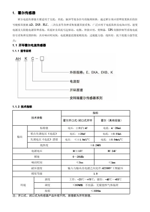
1.霍尔传感器霍尔电流传感器主要适用于交流、直流、脉冲等复杂信号的隔离转换,通过霍尔效应原理使变换后的信号能够直接被AD 、DSP 、PLC 、二次仪表等各种采集装置直接采集,广泛应用于电流监控及电池应用、逆变电源及太阳能电源管理系统、直流屏及直流马达驱动、电镀、焊接应用、变频器,UPS 伺服控制等系统电流信号采集和反馈控制,具有响应时间快,电流测量范围宽精度高,过载能力强,线性好,抗干扰能力强等优点。
1.1开环霍尔电流传感器1.1.1型号说明1.1.2技术指标技术参数指标霍尔开口式/闭口式开环霍尔(真有效值)输出标称值电压:±5V/±4V 电流:4~20mA 零点失调电压(电流)电压:±20mV电流:±0.05mA失调电压(电流)漂移电压:≤±1.0mV/℃电流:±0.04mA/℃线性度≤0.2%FS电源电压DC ±15V DC 24V频宽0~20kHz 响应时间≤5us≤1ms耐压强度输入与输出及电源之间允许AC2500V 工频耐压精度等级1.0环境温度工作:-25℃~+70℃;储存:-40℃~+85℃湿度≤95%RH,不结露,无腐蚀性气体场所海拔≤3500m注:开口式、闭口式为传感器产品外观不同,原理都为开环原理。
1.1.3开口式开环霍尔电流传感器1.1.3.1规格尺寸(单位:mm)图1图21.1.3.2规格参数对照表型号额定电流供电电源额定输出测量孔径(mm)准确度AHKC-EKA 0~(50-500)A ±15V 5V /4V φ201级AHKC-EKAADC 0~(50-500)A12V/24V4~20mAφ201级尺寸规格外形尺寸穿孔尺寸安装尺寸图形W H D a e ΦM N AHKC-EKA 606416//2047/图1AHKC-EKAA 606416//2047/图1AHKC-EKDA 606416//2047/图1AHKC-EKB 10010224//4080/图1AHKC-EKBA 10010224//4080/图1AHKC-EKBDA 10010224//4080/图1AHKC-EKC 11511027//6095.5/图1AHKC-EKCA 11511027//6095.5/图1AHKC-EKCDA 11511027//6095.5/图1AHKC-K 12763256416//30图2AHKC-KAA 12763256416//30图2AHKC-KDA 12763256416//30图2AHKC-H 14979258232//46图2AHKC-KA 17695.52910436//60图2AHKC-HB 204111.52913252//48×2图2AHKC-HBAA 204111.52913252//48×2图2AHKC-HBDA204111.52913252//48×2图2AHKC-EKDA AC 0~(50-500)A 12V/24V 4~20mA φ201级AHKC-EKB 0~(200-1000)A±15V 5V /4V φ401级AHKC-EKBADC 0~(200-1000)A 12V/24V4~20mAφ401级AHKC-EKBDA AC 0~(200~1000)A 12V/24V 4~20mA φ401级AHKC-EKC 0~(500-1500)A±15V 5V /4V φ551级AHKC-EKCADC 0~(500-1500)A 12V/24V4~20mAφ551级AHKC-EKCDA AC 0~(500-1500)A 12V/24V 4~20mA φ551级AHKC-K 0~(400-2000)A±15V 5V /4V 64×161级AHKC-KAA DC 0~(400-2000)A 12V/24V4~20mA64×161级AHKC-KDAAC 0~(400-2000)A12V/24V 4~20mA 64×161级AHKC-H 0~(500-3000)A ±15V 5V /4V 82×321级AHKC-KA 0~(500-5000)A±15V 5V /4V 104×361级AHKC-HB0~(2000-20000)A±15V5V /4V132×521级AHKC-HBAA DC 0~(2000-20000)A12V/24V 4~20mA 132×521级AHKC-HBDA AC 0~(2000-20000)A12V/24V 4~20mA 132×521级注:额定电流未标注表示输入电流交直流均可测量,订货时请注明。

凯利K S L 系列无刷无霍尔电机控制器用户手册适用的产品型号:K S L2L241004100K S L 24241150K S L 24200K S L 24300K S L 36100K S L 36150KSL36200KSL36300KSL48100KSL48150KSL48200KSL48300KSL48400BKSL48500B KSL72100KSL72150KSL72200KSL72300KSL72400BKSL72500B KSL96150KSL96250版本1.22013年4月目录第一章概述 (2)第二章主要特性和规格 (3)2.1基本功能 (3)2.2特性 (3)2.3规格 (4)2.4型号 (4)第三章安装和使用 (5)3.1安装控制器 (5)3.2连线 (6)3.3连接计算机串口 (10)3.4安装时检查 (10)3.5开始使用 (11)第四章维护 (16)4.1清洗 (16)4.2配置 (16)表1:LED错误代码 (17)联系我们: (19)1第一章概述本手册主要介绍凯利公司KSL系列控制器产品的特性,安装使用方法以及维护等方面的知识。
用户在使用凯利控制器之前,请详细阅读本手册,这会帮助您正确的安装和使用凯利控制器。
如果在使用过程中遇到任何问题,请从本文档最后一页查询联系方式与我们联系。
KSL无传感器无刷直流电机驱动控制器由凯利科技投资有限公司自主开发完成,特别适用于风机、水泵、空调压缩机、冰箱压缩机等直流无刷电机和驱动控制的应用场合。
凯利系列控制器采用大功率MOSFET高频设计,效率可达99%。
强大智能的微处理器为凯利系列控制器提供了全面精确的控制。
用户还可以通过我们提供的连接线连接计算机与控制器,自己配置控制器、引导测试并且可以简单快速的获得诊断信息。
2第二章主要特性和规格2.1基本功能(1)扩展的故障检测和保护。
可通过LED闪烁代码来识别故障。
(2)电池电压实时监控。
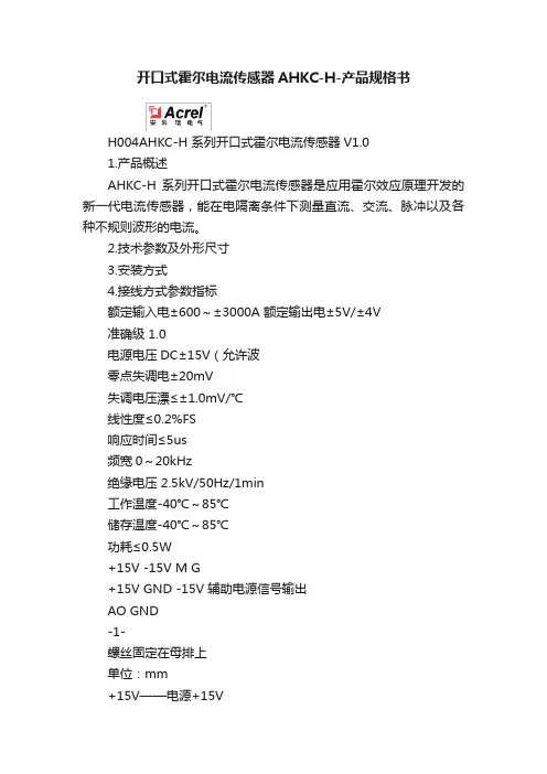
开口式霍尔电流传感器AHKC-H-产品规格书H004AHKC-H 系列开口式霍尔电流传感器V1.01.产品概述AHKC-H 系列开口式霍尔电流传感器是应用霍尔效应原理开发的新一代电流传感器,能在电隔离条件下测量直流、交流、脉冲以及各种不规则波形的电流。
2.技术参数及外形尺寸3.安装方式4.接线方式参数指标额定输入电±600~±3000A 额定输出电±5V/±4V准确级 1.0电源电压DC±15V(允许波零点失调电±20mV失调电压漂≤±1.0mV/℃线性度≤0.2%FS响应时间≤5us频宽0~20kHz绝缘电压 2.5kV/50Hz/1min工作温度-40℃~85℃储存温度-40℃~85℃功耗≤0.5W+15V -15V M G+15V GND -15V 辅助电源信号输出AO GND-1-螺丝固定在母排上单位:mm+15V——电源+15V-15V——电源-15V(注意电源正极与负极不可接反)M——信号输出端正极G——电源地与信号输出端负极注:具体接线按实物外壳上的端子编号为准。
5.注意事项1、霍尔传感器在使用时,为了得到较好的动态特性和灵敏度,必须注意原边线圈和副边线圈之间的耦合,建议使用单根导线且导线完全填满霍尔传感器模块过线孔;2、霍尔传感器在使用时,在额定输入电流值下才能得到最佳的测量精度,当被测电流远低于额定值时,若要获得最佳精度,原边可使用多匝,即:IpNp=额定安匝数。
另外,原边馈线温度不应超过80℃;3、霍尔电流传感器正常工作时的辅助电源不应超过标定值的±20%;4、霍尔电流传感器在安装使用过程中严禁从高处摔落(≥1m);5、不能调节零点、满度调节电位器;6、辅助电源需要自行配置;7、电源正负极不能接反。
6.订货范例例1AHKC-H霍尔电流传感器辅助电源:DC±15V输入:1000A输出:5V精度:1级江苏安科瑞电器制造有限公司联系人:刘丹玲电话:0510-********地址:江苏省江阴市南闸东盟工业园东盟路5号。

Eaton 050075Eaton Moeller® series ZW7 Current transformer-operated overload relay, 420-630A, 1N/O+1N/CAllgemeine spezifikationEaton Moeller® series ZW7 Current transformer-operated overload relay050075162.5 mm97 mm 200.5 mm 0.64 kgIEC/EN 60947 VDE 0660Rated operational current: Switch-on and switch-off conditions based on DC-13, time constant as specified.4015080500759ZW7-630Product NameCatalog Number Product Length/Depth Product Height Product Width Product Weight Certifications Catalog NotesEANModel CodeProtection with heavy starting duty Test/off buttonTrip-free releaseReset pushbutton manual/auto -25 °C50 °C-25 °C40 °COtherDamp heat, constant, to IEC 60068-2-78Damp heat, cyclic, to IEC 60068-2-30IP00Separate positioningSeparate mountingAs required27 mm420 A630 AIII3ZW7 current transformer-operated overload relaysFinger and back-of-hand proof, Protection against direct contact when actuated from front (EN 50274)Features Ambient operating temperature - minAmbient operating temperature - maxAmbient operating temperature (enclosed) - minAmbient operating temperature (enclosed) - maxClassClimatic proofingDegree of protectionMounting methodMounting positionOpening diameterOverload release current setting - minOverload release current setting - maxOvervoltage categoryPollution degreeProduct categoryProtectionRated impulse withstand voltage (Uimp)8000 V AC4000 V (auxiliary and control circuits)10 g, Mechanical, Sinusoidal, Shock duration 10 ms Branch circuits, (UL/CSA)Continuous 2 x (0.75 - 2.5) mm²1 x (0.75 - 2.5) mm²2 x (0.75 - 4) mm²1 x (0.75 - 4) mm²2 x (18 - 14)8 mmM3.5, Terminal screw2, Terminal screw, Pozidriv screwdriver1 x 6 mm, Terminal screw, Control circuit cables, Standard screwdriver1.2 Nm, Screw terminals, Control circuit cables6 A 1.5 A 1.5 A 0.9 A 0.4 A 0.2 A 0.9 A With overload relay in conjunction with a transformer as required for the contactor, Max. Fuse, Main conducting pathsMax. 6 A gG/gL, Fuse, Auxiliary contacts111Shock resistanceSuitable forTemperature compensation Terminal capacity (flexible with ferrule) Terminal capacity (solid)Terminal capacity (solid/stranded AWG) Stripping length (control circuit cable) Screw sizeScrewdriver sizeTightening torqueConventional thermal current ith of auxiliary contacts (1-pole, open)Rated operational current (Ie) at AC-15, 120 VRated operational current (Ie) at AC-15, 220 V, 230 V, 240 V Rated operational current (Ie) at AC-15, 380 V, 400 V, 415 V Rated operational current (Ie) at DC-13, 110 VRated operational current (Ie) at DC-13, 220 V, 230 VRated operational current (Ie) at DC-13, 24 VRated operational current (Ie) at DC-13, 60 V Short-circuit protectionShort-circuit protection ratingNumber of auxiliary contacts (change-over contacts) Number of auxiliary contacts (normally closed contacts) Number of auxiliary contacts (normally open contacts) Number of contacts (normally closed contacts)0.75 A690 V440 V AC, Between auxiliary contacts and main contacts, According to EN 61140240 V AC, Between auxiliary contacts, According to EN 61140 440 V AC, Between main circuits, According to EN 61140B600 at opposite polarity, AC operated (UL/CSA)R300, DC operated (UL/CSA)B300 at opposite polarity, AC operated (UL/CSA)18.1 W0 W2.7 W630 A0 WMeets the product standard's requirements.Meets the product standard's requirements.Meets the product standard's requirements.Meets the product standard's requirements.Meets the product standard's requirements.Does not apply, since the entire switchgear needs to be evaluated.Does not apply, since the entire switchgear needs to be evaluated.Meets the product standard's requirements.Does not apply, since the entire switchgear needs to be evaluated.Rated operational voltage (Ue) - maxSafe isolationSwitching capacity (auxiliary contacts, pilot duty)Number of contacts (normally open contacts)Equipment heat dissipation, current-dependent PvidHeat dissipation capacity PdissHeat dissipation per pole, current-dependent PvidRated operational current for specified heat dissipation (In) Static heat dissipation, non-current-dependent Pvs10.2.2 Corrosion resistance10.2.3.1 Verification of thermal stability of enclosures10.2.3.2 Verification of resistance of insulating materials to normal heat10.2.3.3 Resist. of insul. mat. to abnormal heat/fire by internal elect. effects10.2.4 Resistance to ultra-violet (UV) radiation10.2.5 Lifting10.2.6 Mechanical impact10.2.7 Inscriptions10.3 Degree of protection of assemblies10.4 Clearances and creepage distancesMeets the product standard's requirements.Does not apply, since the entire switchgear needs to beevaluated.Does not apply, since the entire switchgear needs to be evaluated.Is the panel builder's responsibility.Is the panel builder's responsibility.Is the panel builder's responsibility.Is the panel builder's responsibility.Is the panel builder's responsibility.The panel builder is responsible for the temperature rise calculation. Eaton will provide heat dissipation data for the devices.Is the panel builder's responsibility. The specifications for the switchgear must be observed.Is the panel builder's responsibility. The specifications for the switchgear must be observed.The device meets the requirements, provided the information in the instruction leaflet (IL) is observed.eaton-tripping-devices-zw7-characteristic-curve-005.epseaton-tripping-devices-tripping-characteristic-zw7-characteristic-curve.epsDA-DC-00004857.pdfDA-DC-00004847.pdfDA-CE-ETN.ZW7-630IL03407132ZIL04210001ZSortimentskatalog Motoren schalten und schützenDA-CD-zw7DA-CS-zw7eaton-tripping-devices-circuit-zw7-wiring-diagram.epseaton-tripping-devices-current-zw7-dimensions.epseaton-tripping-devices-current-zw7-dimensions-002.epseaton-tripping-devices-current-zw7-3d-drawing.eps10.5 Protection against electric shock10.6 Incorporation of switching devices and components 10.7 Internal electrical circuits and connections10.8 Connections for external conductors10.9.2 Power-frequency electric strength10.9.3 Impulse withstand voltage10.9.4 Testing of enclosures made of insulating material 10.10 Temperature rise10.11 Short-circuit rating10.12 Electromagnetic compatibility10.13 Mechanical function Characteristic curve Declarations of conformity eCAD model Installationsanleitung KatalogemCAD modelSchaltpläne ZeichnungenEaton Konzern plc Eaton-Haus30 Pembroke-Straße Dublin 4, Irland © 2023 Eaton. Alle Rechte vorbehalten. Eaton ist eine eingetrageneMarke.Alle anderen Warenzeichen sindEigentum ihrer jeweiligenBesitzer./socialmedia。

Si721x 场输出霍尔效应磁性位置传感器数据表Silicon Labs 提供的 Si7211/2/3/4/5/6/7 霍尔效应磁性传感器产品系列结合了斩波稳定型霍尔元件以及低噪声模拟放大器、13 位 AD 转换器。
模数转换后,磁场数据可以以模拟、脉冲宽度调制 (PWM)或单边缘渐进传输 (SENT)格式提供(视部件编号而定)。
借助 Silicon Labs 成熟的 CMOS 设计技术,Si721x 产品系列融入数字信号处理,为温度和失调漂移提供精密补偿。
与现有霍尔效应传感器相比,Si721x 产品系列具有行业领先的灵敏度和低噪声,使传感器能够在较大气隙和较小磁体条件下使用。
在最简单的情况下,Si721x 设备以 3 引脚 SOT23 或 TO92 形式封装,提供电源、接地和单输出引脚,该单输出引脚可用于输出对应模拟格式、PWM 或 SENT 格式的磁场信号。
Si721x 设备还提供 5 引脚 SOT23 和 8 引脚 DFN(即将推出)封装形式,除上述引脚外,其他引脚可以用于睡眠模式 (DIS) 或用于启动片上线圈内置自检 (BISTb) 功能。
应用特性:•高灵敏度霍尔效应传感器•与磁场相对应的低噪声输出•为温度和失调漂移提供补偿的集成数字信号处理•睡眠电流消耗低至 50 nA(典型值)•可配置灵敏度、输出极性和采样率•随温度变化,灵敏度漂移幅度 < ±3%•电源电压范围广•1.7 至 5.5 V•3.3 至 26.5 V•可配置输出选项•模拟•PWM•SENT•行业标准封装•表面安装式 SOT-23(3 引脚或 5 引脚)封装•TO92 封装•DFN 封装(即将推出)•消费、工业和汽车应用中的机械位置传感器•相机影像稳定、放大和自动聚焦•液位感应•控制旋钮和选择器开关DIS (Optional)VOUTVDD VDDTable of Contents1.Electrical Specifications (3)2.Functional Description (9)3.Analog Output (10)4.PWM Output Description (11)5.SENT Output (12)5.1 tSENT Status Nibble (12)5.2 SENT Data Nibbles (13)5.3 CRC Calculation (13)5.4 SENT Pause Pulse (13)5.5 SENT Frame Rate (13)5.6 BIST Activation During SENT Operation (13)6.Pin Description (14)7.Ordering Guide (16)8.Package Outline (18)8.1 SOT23 3-Pin Package (18)8.2 SOT23-5 5-Pin Package (20)8.3 TO92S 3-Pin Package (22)nd Patterns (23)9.1 SOT23 3-Pin PCB Land Pattern (23)9.2 SOT23-5 5-Pin PCB Land Pattern (24)10.Top Marking (25)10.1 SOT23 3-Pin Top Marking (25)10.2 SOT23-5 5-Pin Top Marking (26)10.3 TO92 Top Marking (26)11.Revision History (27)1.Electrical SpecificationsUnless otherwise specified, all min/max specifications apply over the recommended operating conditions.Table 1.1. Recommended Operating ConditionsTable 1.2. General Specification1Table 1.3. Output Pin SpecificationsTable 1.4. Magnetic SensorTable 1.5. Temperature CompensationTable 1.6. Thermal CharacteristicsTable 1.7. Absolute Maximum Ratings1Functional Description 2. Functional DescriptionThe Si7211/2/3/4/5/7 family of Hall Effect magnetic sensors digitize the component of the magnetic field in the z axis of the device (pos-itive field is defined as pointing into the device from the bottom). The digitized field is then converted to an output format of analog, PWM or SENT and presented on the output pin.Table 2.1. Part DescriptionRefer to the Magnetic Sensors Selector Guide for the two digit number after the die revision which gives more details about output, sampling frequency and other details.Data output is always unsigned. That is, half scale (V DD/2 for analog out parts, 50% duty cycle for PWM output parts and 2048 (0x800) for SENT output parts) corresponds to zero field.The parts are preconfigured for the magnetic field measurement range, idle time, temperature compensation and digital filtering and will wake into this mode when first powered. The specific configuration output type (open collector or push pull) are determined by the part number.Analog Output 3. Analog OutputFor the Si7211, the analog output is V DD/2 at zero field and goes from nearly zero at large negative field to nearly V DD at large positive field.B(mT)=(20.47or204.7)×(2×Vout Vdd−1)4- and 5-pin packages also have the option of a BISTb pin. When configured and detected low, the internal coil is turned on until the pin is detected high again. Each subsequent BISTb activation flips the polarity of the coil during BIST.For high voltage parts (Si7216), the output is ratiometric to an internally derived V DD of 5V (± 5%) so long as the input V DD is > 6 V.B(mT)=(20.47or204.7)×(2×Vout5−1)For V DD < 6 V the internally derived reference drops 1 V for each 1 V drop in V DD to the minimum recommended working voltage of 4.0 V.PWM Output Description 4. PWM Output DescriptionThe PWM output can be configured as open drain or push pull. High voltage parts can only be configured as open drain. The PWM duty cycle is factory configured and is normally set to in the range of 10 Hz to 1 KHz and is ±5%. See ordering guide for specific part num-bers..As each measurement completes, the next PWM cycle will be updated to reflect the last measurement result. The duty cycle varies from 0 to 100% where 50% duty cycle means zero field, 0 % duty cycle generally means maximum negative field (-20.47 mT or -204.7 mT) and 100% duty cycle generally means maximum positive field (+20.47 or +204.7 mT). The high portion of the PWM is output first so thatB(mT)=(20.47or204.7)×(2×Thigh−1)Thigh+TlowThe host processor should look for a variation in the magnetic field to determine the entire system is working properly.4- and 5-pin packages also have the option of a BISTb pin. When configured and detected low the internal coil is turned on until the pin is detected high again. Each subsequent BISTb activation flips the polarity of the coil during BIST.5. SENT OutputThe Si7213 and Si7215 output data in SENT (Single Edge Nibble transmission) format conforming to J2716 January 2010. All SENT output parts are configured as open collector.SENT protocol messages consist of:• A calibration/synchronization period consisting of 56 clock ticks• A status and serial communication 4-bit nibble• A sequence of up to six data nibbles• A one nibble checksum•Each nibble is 12 to 27 clock ticks•An optional delay pause pulseFigure 5.1. SENT Timing DiagramAs can be seen, each part of the sequence is determined by the timing between falling edges of the open drain sent output. First, a time of 56 clock ticks is produced so that the receiver can calibrate itself to the Si7213/5 speed. Then a total of 8 nibbles (4 bits per nibble) is produced. The edge to edge time of each nibble is 12 clock ticks for a data nibble of 0000b 13 ticks for a data value of 0001b and so on up to 27 ticks for a data value of 1111b.The nominal tick time has been standardized at 5 μsec (±5%) however this is configurable.5.1 tSENT Status NibbleIn the Si721x the four bit status nibble is defined as follows:•Bit 3 and Bit 2 always transmitted as zeroes (No serial message support)•Bit 1 and Bit 0•00 Normal; No error condition•01 Error condition•10 Positive field BIST active•11 Negative field BIST active5.2 SENT Data NibblesThe Si7213 and Si7215 are configurable to support a variety of options. The standard option follows J2716 A.3 where:For magnetic field, 3 nibbles are put together for a total 12 bit data word with values that can range from 0 to 4095. For magnetic field data, 2048 corresponds to zero field. The Si7213 can be configured for ± 20.47 mT full scale or ± 204.7 mT full scale. On the 20.47 mT full scale 1 LSB is 0.01 mT and on the 204.7 mT full scale 1 LSB is 0.1 mT.5.3 CRC CalculationThe CRC is calculated based on the 6 data nibble according to x4 +x3 + x2 + 1 with a seed value of 0101 as per the recommendations in J7216 section 5.4.2.2. The legacy CRC calculation is not supported.5.4 SENT Pause PulseThe Si7213 and Si7215 are configurable for a pause pulse that is 12 ticks low, 256 ticks wide. However, the standard offering is no pause pulse.5.5 SENT Frame RateFor the standard offering with no pause pulse, each message will be 154 to 270 ticks in length. At a tick time of 5 μsec this is 770 to 1350 μsec. This gives an average frame rate of approximately 1 msec for the standard tick time of 5 μsec. Conversion start is synchronized to the start of the synch pulse and is normally completed before the synch pulse completes so the data that is reported is the data obtained during the synch pulse time.5.6 BIST Activation During SENT OperationFor 3-pin packages BIST can be activated by holding the output pin low for the entire message.Once BIST is activated SENT messages resume 12 ticks after the SENT IO pin is detected high. Eight positive field BIST messages are followed by eight negative field BIST messages followed by a return to normal messages.The nominal magnetic field output of the on-chip generator varies with coil current. The coil current varies with the coil resistance and power supply voltage, so the nominal magnetic field output varies according to:Bout = BperVnom x VDDBperVnom is 1.6 mT/VThis can be used to calculate the expected magnetic field from the test coil for a given V DD. This is somewhat temperature dependent, so the actual measured field will vary according to the accuracy of the part as well as temperature. Generally, as the coil is turned on and off the measured variation in field should be within ±25% of expectation based on the calculated field generation.The host processor should look for a variation in the magnetic field output to determine the entire system is working properly.The 4- and 5-pin packages also have the option of a BISTb pin. When configured and detected low, the internal coil is turned on until the pin is detected high again. Each subsequent BISTb activation flips the polarity of the coil during BIST.6. Pin Description123TO-92, 3-PinFront ViewSOT-23, 5-PinTop ViewSOT-23, 3-Pin Top View Figure 6.1. Si721x Pin AssignmentsNote:The 3-pin option includes part numbers: Si7211/12/13/14/15/16.The SOT-23 5 pin option include part numbers: Si7217.Table 6.1. Si7211/12/13/14/15/16 (SOT23 3-pin Package)Table 6.2. Si7217 (SOT23 5-pin Package)Table 6.3. Si7211 (TO-92 Package)7. Ordering GuideSi721B F V Rxx Silicon Labs Magnetic Sensor Family Output TypeRevision Feature Set MinorTemperature GradePackageTape and Reel (Optional)See Selector Guide for breakdown of feature setV = SOT23, B = TO92, M = DFN8xFeature Set Major1, 6, 7 = Analog 2, 4 = PWM F = (0 to +70)I = (-40 to +125)3, 5 = SENTFigure 7.1. Si721x Part NumberingTable 7.1. Product Selection GuideAdditional InformationFor information on the below specifications of each OPN refer to the Magnetic Sensors Selector Guide:•Current consumption•Built in self test if applicableAll Si721x parts periodically measure the field and output the data in PWM, SENT, or analog format.The Si721x parts are factory configurable for:•The type of output analog, SENT, or PWM•The amount of digital filtering applied to the samples•The time between measurements•The output pin can be open drain or push pull (SENT and PWM parts)•Full scale can be programmed as 20mT or 200mT• A temperature compensation can be applied to the field data to adjust for the variation in field with temperature for common magnet typesNote: North pole of a magnet at the bottom of a SOT23 package, top of a DFN 8 package(coming soon), or front of a TO92 pack-age(coming soon) is defined as positive field.8. Package Outline 8.1 SOT23 3-Pin PackageTable 8.1. SOT23 3-Pin Package Dimensions8.2 SOT23-5 5-Pin PackageTable 8.2. SOT23-5 5-Pin Package Dimensions8.3 TO92S 3-Pin PackageTable 8.3. TO92S 3-Pin Package Dimensions9. Land Patterns9.1 SOT23 3-Pin PCB Land Pattern9.2 SOT23-5 5-Pin PCB Land Pattern10. Top Marking10.1 SOT23 3-Pin Top MarkingNote: TTTT is a manufacturing code.10.2 SOT23-5 5-Pin Top MarkingNote: TTTT is a manufacturing code.10.3 TO92 Top MarkingNote: TTTT is a manufacturing code. PPPP is 72xx.Revision History 11. Revision HistoryRevision 1.3May, 2020•Added EOL note for Si7214/15/16 in the Ordering Guide (200324717 End of Life Notification for High Voltage Si72xx Devices). Revision 1.2March, 2019•Removed all mention of AEC-Q100 qualification in product description and feature list.Revision 1.1October 11th, 2018•Added Si7211 TO92 part number.•Added details on Si7217 part number.•Added specifications for Si7217.Revision 1.0January 4, 2018•Updated power numbers to be consistent with production test limits.•Moved detailed ordering guide to a separate selection guide.•Updated detailed description to be clearer and more accurate.Revision 0.9June 30, 2017•Updated 1. Electrical Specifications.•Updated 7. Ordering Guide.•Minor typo corrections.Revision 0.1February 1, 2016•Initial release.Smart. Connected. Energy-Friendly.Products /productsQuality/qualitySupport and CommunitySilicon Laboratories Inc.400 West Cesar ChavezAustin, TX 78701USADisclaimerSilicon Labs intends to provide customers with the latest, accurate, and in-depth documentation of all peripherals and modules available for system and software implementers using or intending to use the Silicon Labs products. Characterization data, available modules and peripherals, memory sizes and memory addresses refer to each specific device, and "Typical" parameters provided can and do vary in different applications. Application examples described herein are for illustrative purposes only. Silicon Labs reserves the right to make changes without further notice to the product information, specifications, and descriptions herein, and does not give warranties as to the accuracy or completeness of the included information. Without prior notification, Silicon Labs may update product firmware during the manufacturing process for security or reliability reasons. Such changes will not alter the specifications or the performance of the product. Silicon Labs shall have no liability for the consequences of use of the information supplied in this document. This document does not imply or expressly grant any license to design or fabricate any integrated circuits. The products are not designed or authorized to be used within any FDA Class III devices, applications for which FDA premarket approval is required, or Life Support Systems without the specific written consent of Silicon Labs. A "Life Support System" is any product or system intended to support or sustain life and/or health, which, if it fails, can be reasonably expected to result in significant personal injury or death. Silicon Labs products are not designed or authorized for military applications. Silicon Labs products shall under no circumstances be used in weapons of mass destruction including (but not limited to) nuclear, biological or chemical weapons, or missiles capable of delivering such weapons. Silicon Labs disclaims all express and implied warranties and shall not be responsible or liable for any injuries or damages related to use of a Silicon Labs product in such unauthorized applications.Trademark InformationSilicon Laboratories Inc.®, Silicon Laboratories®, Silicon Labs®, SiLabs® and the Silicon Labs logo®, Bluegiga®, Bluegiga Logo®, Clock B uilder®, CMEMS®, DSPLL®, EFM®, EFM32®, EFR, Ember®, Energy Micro, Energy Micro logo and combinations thereof, "the world’s most energy friendly microcontrollers", Ember®, EZLink®, EZRadio®, EZRadioPRO®, Gecko®, Gecko OS, Gecko OS Studio, ISOmodem®, Precision32®, ProSLIC®, Simplicity Studio®, SiPHY®, Telegesis, the Telegesis Logo®, USBXpress® , Zentri, the Zentri logo and Zentri DMS, Z-Wave®, and others are trademarks or registered trademarks of Silicon Labs. ARM, CORTEX, Cortex-M3 and THUMB are trademarks or registered trademarks of ARM Holdings. Keil is a registered trademark of ARM Limited. Wi-Fi is a registered trademark of the Wi-Fi Alliance. All other products or brand names mentioned herein are trademarks of their respective holders.。
霍尔基础介绍霍尔效应原理电流Is通过N型或P型霍尔元件,磁场B方向与电流Is方向垂直,且磁场方向由内向外,对于N型半导体及P型半导体,分别产生的方向如左图和右图的霍尔电场EH。
霍尔电势差E H会阻止载流子继续向侧面偏移,当载流子所受的横向电场力F E与洛仑兹力F B相等时,上下两侧电荷的积累就达到动态平衡。
因为:F E=eE H,F B=evB,则:E H=vB又因为:I S=nevbd其中b为宽,d为厚度,n为载流子浓度带入公式得到霍尔电势:Uh=E H b=BIs/nedUh=K H*Is*B其中KH=1/ned,KH被称为霍尔元件的霍尔系数*霍尔电势Uh与控制电流Is 及磁感应强度B成正比霍尔元件•霍尔元件常见半导体材料:霍尔元件温度特性InSb霍尔一般工作在恒压模式,温度特性好GaAs霍尔一般工作在恒流模式,温度特性好开环霍尔电流传感器◆开环霍尔电流传感器由磁芯和放置在磁芯开口气隙内的霍尔元件组成。
载流导体穿过磁芯中心孔,它将产生一个和其电流成比例的磁场。
这个磁场被磁芯集中并被霍尔元件检测到。
大部分开环电流传感器含有温度补偿的电子线路,它输出一个经过校正的电压输出。
◆开环电流传感器测量直流和交流电流并提供被测电流和输出电压之间的电气隔离。
开环传感器的典型功耗远小于闭环传感器。
它们是在电池供电的要求功耗较小的系统中最优的选择。
◆还有一种叫法叫直放式电流传感器开环霍尔电流传感器原理图开环单电源电路开环双电源电路开环电流传感器--特点•体积小•重量轻•测量范围宽•低能量损耗•无插入损耗•结构简单,可靠性高闭环霍尔电流传感器◆闭环霍尔电流传感器主要由磁芯、放置在磁芯开口气隙内的霍尔元件、环绕铁芯的线圈和一个电流放大器组成。
载流导线穿过磁芯中心孔,它将产生一个和其电流成比例的磁场。
这个磁场被磁芯集中并被传送到霍尔元件检测。
霍尔传感器及电流放大器产生与检测电流成比例的输出电流,它驱动线圈产生反向磁场。
罗克韦尔自动化 42KD-IN001A-ZH-P — 2014 年 10 月42KD 微型传感器安装说明翻译自原版说明描述42KD 微型传感器为空间非常狭小的应用提供了解决方案。
42KD 传感器是光电传感器产品组合中最小的传感器。
它提供多种传感模式、多种检测距离,以及自动 PNP/NPN 功能、按钮/远程示教功能和按钮锁定选项。
尽管体积小巧,但其性能和特性很可靠,极具竞争优势。
42KD 提供可见红色 LED 型号,以及偏振反射式和固定/可调式背景抑制传感模式。
示教按钮可简化设置过程,甚至还支持从远程对传感器进行示教。
该传感器还支持选择明操作 (L.O.) 或暗操作 (D.O.)。
所有 42KD 传感器都具有特有的“自动 PNP/NPN”输出,可以降低库存成本,简化选型、安装和维护工作。
对于包括自动化、包装和物料输送领域在内的众多应用而言,42KD 传感器都是一个极佳的解决方案。
借助以上这些特性,42KD 传感器可轻松适用于各项具有挑战性的应用,而且尤其适合于空间有限的应用。
特征•罗克韦尔自动化产品组合中最小的传感器•自动 NPN/PNP 输出•通过示教按钮轻松设置切换点•外部示教功能•IP67 外壳•完备的独立传感器•产品随附安装配件请保存本说明,以备后用。
重要信息技术规格接线图引脚输出下图显示的是快速断开接头。
引脚编号与传感器上的公接头相对应。
认证CE 标记,满足所有适用指令外壳类型等级IP67工作温度 [C(F)]-20…+50° (-4…+122°)存储温度 [C(F)]-20…+80° (-4…+176°)振动10…55 Hz ,1 mm 振幅,满足 IEC 60947-5-2 要求或达到更高水平冲击30 g ,脉冲持续时间 11 ms ,满足 IEC 60947-5-2 要求或达到更高水平光学LED 指示灯绿色:工作电压开启;黄色:检测到对象/正在启动输出电气工作电压10…30V DC 空载电流LED 型号:≤30 mA保护类型短路和反极性输出响应时间500 μs输出类型自动 NPN/PNP输出功能额外支持通过按钮和远程示教来启用明操作和暗操作(固定背景抑制型号);额外支持通过远程示教启用明操作和暗操作输出电流≤50 mA开关频率1,000 Hz机械外壳材料PUR 镜头材料PMMAPNP 模式NPN 模式M8 公头罗克韦尔自动化 42KD-IN001A-ZH-P — 2014 年 10 月2 42KD 微型传感器尺寸 [mm (in.)]示教接口默认设置:出厂默认设置如下:传感范围:最大设置输出类型:自动 PNP/NPN 。
NSM2012 基于霍尔原理,高精度,具有共模磁场抑制,可达3000V隔离的电流传感器Datasheet (CN) 1.0Product OverviewNSM2012是一款集成路径电流传感器,具有1.2mΩ极低的导通电阻,减少了芯片上的热损耗。
纳芯微创新的隔离技术以及信号调理设计能够满足高隔离等级的同时感测流过内部B usbar的电流。
内部采用差分霍尔对,因此对外部杂散磁场有很强的抵御能力。
NSM2012支持比例输出和固定输出模式,固定模式方便客户ADC差分采样Vref以及Vout的电压以减少外部共模干扰(比如温度等)。
对比同样Shunt+隔离运放的电流采样方式,NSM2012省去了原边供电并且Layout简单方便,同时具有极高隔离耐压以及Lifetime稳定性。
在高边电流检测应用中只需用一颗NSM2012即可达到600V pk工作电压,无需加任何保护器件即可耐受6kV浪涌电压。
由于NSM2012内部精确的温度补偿算法以及出厂精度校准,此电流传感器在全温度工作范围都可以保持很好的精度,客户无需做二次编程。
支持3.3V/5V供电电压(不同供电版本)。
Key Features•高带宽以及快速响应时间•400kHz带宽• 1.5us响应时间•高精度电流测量•差分霍尔检测可抵御外界杂散磁场•满足UL标准的高隔离等级•耐受隔离耐压(V ISO):3000Vrms•最大浪涌隔离耐压(V surge):6kV•CMTI > 100V/ns•CTI(I)•爬电距离/电气间距:4mm•纳芯微创新的斩波以及旋转电流激励技术使得零点温漂很小•比例输出或者固定输出•工作温度:-40℃ ~ 125℃•原边导通电阻:1.2mΩ•SOIC8封装•满足UL62368/EN62368安规认证•ROHSApplications•光伏•工业电源•电机控制•OBC/DCDC/PTC Heater•充电桩Device InformationFunctional Block DiagramsFigure 1. NSM2012 Block DiagramINDEX1. PIN CONFIGURATION AND FUNCTIONS (3)2. ABSOLUTE MAXIMUM RATINGS (4)3. ISOLATION CHARACTERISTICS (4)4. SPECIFICATIONS (5)4.1C OMMON C HARACTERISTICS (TA=-40°C TO 125°C,VCC=5V OR 3.3V, UNLESS OTHERWISE SPECIFIED) (5)4.2NSM2012-30B3R-DSPR C HARACTERISTICS (TA=-40°C TO 125°C,VCC=3.3V, UNLESS OTHERWISE SPECIFIED) (6)4.3NSM2012-30B5R-DSPR C HARACTERISTICS (TA=-40°C TO 125°C,VCC=5V, UNLESS OTHERWISE SPECIFIED) (6)4.4NSM2012-10U5R-DSPR C HARACTERISTICS (TA=-40°C TO 125°C,VCC=5V, UNLESS OTHERWISE SPECIFIED) (7)4.5NSM2012-20B5R-DSPR C HARACTERISTICS (TA=-40°C TO 125°C,VCC=5V, UNLESS OTHERWISE SPECIFIED) (8)4.6T YPICAL P ERFORMANCE C HARACTERISTICS (9)NSM2012-30B3R-DSPR[1] (9)NSM2012-30B5R-DSPR[1] (9)NSM2012-10U5R-DSPR[1] (10)NSM2012-20B5R-DSPR[1] (11)5. FUNCTION DESCRIPTION (13)5.1.O VERVIEW (13)5.2.NSM2012R版本(单端比例输出) (13)5.3.NSM2012F版本(固定输出版本) (13)5.4.NSM2012专业术语定义 (13)6. APPLICATION NOTE (16)6.1.典型应用电路 (16)6.2.PCB L AYOUT (16)6.3.热评估实验 (17)7. PACKAGE INFORMATION (18)8. ORDER INFORMATION (19)9. TAPE AND REEL INFORMATION (20)10. REVISION HISTORY (21)1. Pin Configuration and FunctionsR Version F VersionFigure 1.1 NSM2012 PackageTable 1.1 NSM2012 Pin Configuration and Description2.Absolute Maximum Ratings3.Isolation Characteristics4.Specifications[1]: 被设计保证。
数据手册概述SDC177MJJ是一款单极型的开关霍尔集成电路,内置反向保护电路,电压稳压器,霍尔电压发生器,差分放大器,史密特触发器和集电极开路输出,能将变化的磁场信号转换成数字信号输出。
它可应用于麻将机、速度测量等场合。
特点⏹工作电压范围宽:3.5V~20V ⏹内含温度补偿电路⏹集电极开路输出⏹最大25mA的输出电流⏹封装形式:TO-92S应用⏹麻将机⏹电子开关⏹速度测量图1. 封装形式TO-92SS D CD EN TI ALD OC UME NT数据手册管脚描述GND VCCOUT Package: TO-92S图2. 管脚排布编号 名称 功能 1 VCC工作输入电源2 GND地 3OUT输出脚表1. 管脚描述功能框图OUT图3. 功能框图SN T I AL D OCUM EN T数据手册订购信息SDC177MJJ Circuit TypePackage TO-92S: ZSE1: Pb-freeG1: Halogen-free X X -XMagnetic Characteristics: A/B/C/DX TR: Tape Reel Blank: Tube封装 温度范围产品编号标识编号包装 形式 无铅 无卤无铅 无卤 TO-92S -20℃~85℃SDC177MJJBZS-E1 SDC177MJJBZS-G1177M 177MG 袋装 SDC177MJJCZS-E1SDC177MJJCZS-G1 177M 177MG 袋装 SDC177MJJDZS-E1SDC177MJJDZS-G1177M 177MG 袋装 SDC177MJJBZSTR-E1 SDC177MJJBZSTR-G1 177M 177MG 编带 SDC177MJJCZSTR-E1 SDC177MJJCZSTR-G1 177M 177MG 编带 SDC177MJJDZSTR-E1SDC177MJJDZSTR-G1177M177MG编带SD CCO NFID E N T I AL D OCUM EN T数据手册极限参数(注意:应用不要超过最大值,以防止损坏。