txs0102 电平转换芯片
- 格式:pdf
- 大小:583.00 KB
- 文档页数:20
txs0108e 原理
TXS0108E是一种8位级电压级转换器,通常用于在不同电压域之间进行逻辑电平转换。
它具有多种功能和特性,其原理涉及到几个方面。
首先,TXS0108E的原理之一是电压级转换。
它能够将高电平转换为低电平,反之亦然。
这意味着当输入端的电压高于VCC1时,TXS0108E会将其转换为VCC2的电平输出,反之亦然。
这种功能使得它在不同电压领域之间进行信号传输时非常有用。
其次,TXS0108E还具有双向传输功能。
这意味着它可以同时处理从A端到B端和从B端到A端的信号传输。
这种双向传输的特性使得它在双向通信系统中非常实用,例如I2C总线通信。
此外,TXS0108E还内置了电流保护功能,可以保护芯片免受短路和过电流的损害。
这使得它在复杂电路中更加可靠和安全。
另外,TXS0108E还具有低功耗特性,这使得它在便携设备和电池供电系统中能够节省能源,延长电池寿命。
总的来说,TXS0108E通过电压级转换、双向传输、电流保护和低功耗等原理,实现了在不同电压领域之间可靠、安全、高效地进行信号传输和通信的功能。
这些原理使得TXS0108E在电子设备中得到广泛应用,特别是在需要进行电压级转换和双向通信的场合。

双向电平转换芯片的参数介绍双向电平转换芯片是一种常用的电子元件,用于在不同电平之间进行转换和传递信号。
它可以将高电平转换为低电平,也可以将低电平转换为高电平,实现不同电平之间的互联和通信。
本文将对双向电平转换芯片的参数进行介绍。
我们来了解一下双向电平转换芯片的工作原理。
双向电平转换芯片通常由两个部分组成:输入端和输出端。
输入端接收来自外部的信号,输出端将信号传递给外部设备。
双向电平转换芯片通过内部电路将输入端的信号转换为输出端的信号,并确保信号在传递过程中保持稳定和准确。
在介绍双向电平转换芯片的参数之前,我们先来了解一下常见的电平标准。
常见的电平标准有TTL、CMOS和LVCMOS等。
TTL (Transistor-Transistor Logic)电平标准是一种数字电平标准,逻辑高电平为5V,逻辑低电平为0V。
CMOS(Complementary Metal-Oxide-Semiconductor)电平标准也是一种数字电平标准,逻辑高电平为Vcc(供电电压),逻辑低电平为0V。
LVCMOS(Low-Voltage CMOS)电平标准是一种低电压数字电平标准,逻辑高电平和逻辑低电平的电压范围根据具体型号而定。
接下来,我们来介绍一些常见的双向电平转换芯片参数。
1. 供电电压(Vcc):双向电平转换芯片的工作电压范围,一般为3.3V、5V或其他供电电压。
2. 逻辑电平转换:双向电平转换芯片能够将输入端的逻辑高电平转换为输出端的逻辑高电平,并将逻辑低电平转换为逻辑低电平,确保信号的准确传递。
3. 带宽:双向电平转换芯片的带宽指的是其能够传递的最高频率信号,通常以MHz为单位。
4. 上升时间和下降时间:双向电平转换芯片的上升时间和下降时间是指信号从逻辑低电平到逻辑高电平或从逻辑高电平到逻辑低电平的转换时间,一般以纳秒为单位。
5. 输入和输出电阻:输入电阻是指双向电平转换芯片输入端对外部信号的阻抗,输出电阻是指双向电平转换芯片输出端对外部设备的阻抗。
电平转换芯片内部原理
电平转换芯片是一种常见的电子元器件,它可以将输入的电信号转换为特定的电平输出信号,以满足各种电子产品对电平转换的需求。
其内部原理是通过使用特定的逻辑电路和模拟电路,在输入信号和输出信号之间建立一个适当的转换桥梁。
电平转换芯片主要分为数字电平转换芯片和模拟电平转换芯片
两种类型。
数字电平转换芯片内部包含多个逻辑门电路,可以将输入的数字信号转换为特定的数字电平输出信号,比如将3.3V的数字信
号转换为5V的数字信号。
而模拟电平转换芯片则通过运用模拟电路
来实现输入信号和输出信号之间的电平转换,比如将低电平输入信号转换为高电平输出信号。
电平转换芯片内部的核心器件是转换管,它是一种特殊的双极性晶体管。
当输入信号满足一定电平条件时,转换管会将其转化为输出信号。
同时,为了保证转换管的稳定性和可靠性,电平转换芯片内部通常还包括电源管理电路、过压保护电路、温度补偿电路等辅助电路。
总的来说,电平转换芯片通过逻辑电路和模拟电路实现不同电平之间的转换,从而满足不同电子产品对电平转换的需求。
其内部结构和原理的精细设计和制造,为现代电子技术的发展和应用提供了重要的技术支持。
- 1 -。
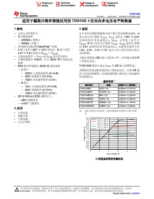
适用于漏极开路和推挽应用的 TXS0104E 4 位双向多电压电平转换器1 特性•无需方向控制信号•最大数据速率–24Mbps(推挽)–2Mbps(开漏)•采用德州仪器 (TI) NanoFree™封装• A 端口支持 1.65V 至 3.6V 的电压,B 端口支持2.3V 至 5.5V 的电压 (V CCA≤ V CCB)•无需电源排序– V CCA或 V CCB均可优先斜升•闩锁性能超过 100mA,符合 JESD 78 II 类规范的要求•ESD 保护性能超过 JESD 22 规范要求–A 端口•2000V 人体放电模型 (A114-B)•200V 机器模型 (A115-A)•1000V 充电器件模型 (C101)–B 端口•15kV 人体放电模型 (A114-B)•200V 机器模型 (A115-A)•1000V 充电器件模型 (C101)•IEC 61000-4-2 ESD(B 端口)–±8kV 接触放电–±10kV 气隙放电2 应用•手持终端•智能手机•平板电脑•台式计算机3 说明这个 4 位同相转换器使用两个独立的可配置电源轨。
A 端口设计用于跟踪 V CCA。
V CCA支持从 1.65V 到 3.6V 范围内的任意电源电压。
V CCA必须低于或等于V CCB。
B 端口旨在用于跟踪 V CCB。
V CCB支持从 2.3V 到5.5V 范围内的任意电源电压。
这使得该器件可在 1.8V、2.5V、3.3V 和 5V 电压节点之间任意进行低压双向转换。
当输出使能端 (OE) 输入为低电平时,所有输出都被置于高阻抗状态。
TXS0104E 被设计成由 V CCA为 OE 输入电路供电。
为确保在加电或断电期间处于高阻抗状态,应将 OE 通过下拉电阻器接地;该电阻器的最小值取决于驱动器的拉电流能力。
(1)(1)如需了解所有可用封装,请参阅数据表末尾的可订购产品附录。
OutputVoltage(V)Input Voltage (V)C001N 沟道晶体管的传输特征内容1 特性...................................................................................12 应用...................................................................................13 说明...................................................................................14 修订历史记录.....................................................................25 引脚配置和功能.................................................................4引脚功能:ZXU/ NMN.......................................................4引脚功能:DSBGA...........................................................5引脚功能:D 、PW 或 RGY...............................................66 规格...................................................................................76.1 绝对最大额定值...........................................................76.2 ESD 等级....................................................................76.3 建议运行条件..............................................................86.4 热性能信息:ZXU 、YZT 和 NMN...............................86.5 热性能信息:D 、PW 和 RGY.....................................96.6 电气特性......................................................................96.7 时序要求:V CCA = 1.8V ± 0.15V...............................106.8 时序要求:V CCA = 2.5V ± 0.2V.................................106.9 时序要求:V CCA = 3.3V ± 0.3V.................................106.10 开关特性:V CCA = 1.8V ± 0.15V.............................116.11 开关特性:V CCA = 2.5V ± 0.2V...............................136.12 开关特性:V CCA = 3.3V ± 0.3V...............................156.13 典型特性..................................................................167 参数测量信息...................................................................177.1 负载电路.. (17)7.2 电压波形....................................................................188 详细说明..........................................................................198.1 概述...........................................................................198.2 功能方框图................................................................198.3 特性说明....................................................................208.4 器件功能模式............................................................209 应用和实现.......................................................................219.1 应用信息....................................................................219.2 典型应用....................................................................2110 电源相关建议.................................................................2311 布局................................................................................2411.1 布局布线指南...........................................................2411.2 布局示例..................................................................2412 器件和文档支持.............................................................2512.1 文档支持..................................................................2512.2 接收文档更新通知...................................................2512.3 社区资源..................................................................2512.4 商标.........................................................................2513 接收文档更新通知..........................................................2514 支持资源........................................................................2515 静电放电警告.................................................................2516 术语表............................................................................2517 机械、封装和可订购信息.. (25)4 修订历史记录注:以前版本的页码可能与当前版本的页码不同Changes from Revision H (May 2018) to Revision I (October 2020)Page•更新了整个文档的表、图和交叉参考的编号格式................................................................................................1•添加了 NMN 封装 12 引脚 nFBGA......................................................................................................................4Changes from Revision G (September 2017) to Revision H (May 2018)Page•更改了开关特性:V CCA = 3.3V ± 0.3V 表中最大数据速率的最大值..................................................................15Changes from Revision F (December 2014) to Revision G (September 2017)Page•更改了“器件信息”表........................................................................................................................................1•通篇删除了 GXU 引用.........................................................................................................................................4•在绝对最大额定值 中添加了结温........................................................................................................................7•重新编排了电气特性 ..........................................................................................................................................9•将电压转换基础知识 添加到“相关文档”........................................................................................................25•添加了接收文档更新通知 和社区资源 (25)Changes from Revision E (August 2013) to Revision F (December 2014)Page•添加了引脚配置和功能 部分、处理等级 表、特性说明 部分、器件功能模式、应用和实施 部分、电源相关建议 部分、布局 部分、器件和文档支持 部分以及机械、封装和可订购信息 部分......................................................1•从“绝对最大额定值”表中删除了封装热阻信息,并将其添加到“热性能信息”表中将 T stg 行移到了新的“处理额定值”表中...................................................................................................................................................7•将第一个开关特性表中最后 2 行的“最小值最大值”中的最大值 24 和最大值 2 更改到最小值列. (11)TXS0104EZHCSI61I – JUNE 2006 – REVISED OCTOBER 2020Changes from Revision D (May 2008) to Revision E (August 2013)Page•删除了订购表 (1)TXS0104EZHCSI61I – JUNE 2006 – REVISED OCTOBER 20205 引脚配置和功能图 5-1. ZXU 封装顶视图图 5-2. NMN 顶视图引脚功能:ZXU/ NMNTXS0104EZHCSI61I – JUNE 2006 – REVISED OCTOBER 2020图 5-3. YZT 封装 12 引脚 DSBGA 顶视图引脚功能:DSBGATXS0104EZHCSI61I – JUNE 2006 – REVISED OCTOBER 20201147823456131211109B1B2B3B4NCA1A2A3A4NCO EV G N DC C BV C C ANC - 无内部连接图 5-4. RGY 封装 14 引脚 VQFN 顶视图NC - 无内部连接图 5-5. D 和 PW 封装 14 引脚 SOIC 和 TSSOP 顶视图引脚功能:D 、PW 或 RGYTXS0104EZHCSI61I – JUNE 2006 – REVISED OCTOBER 20206 规格6.1 绝对最大额定值(1)(1)应力超出绝对最大额定值 下所列的值可能会对器件造成损坏。
双向电平转换芯片的参数介绍双向电平转换芯片是一种常用的电子元件,用于将不同电平之间进行转换。
它在数字电路中起到了重要的作用,能够实现不同电平之间的平滑过渡,确保电路的正常运行。
本文将就双向电平转换芯片的参数进行介绍。
我们来了解一下双向电平转换芯片的工作原理。
双向电平转换芯片可以将低电平转换为高电平,也可以将高电平转换为低电平。
其内部结构包含输入输出端口、电平转换电路和控制逻辑电路。
当输入端口的电平发生变化时,电平转换电路会进行相应的转换,并将转换后的电平输出到输出端口。
控制逻辑电路则负责控制电平的转换过程,确保电路能够按照预定的规则进行运行。
接下来,我们来介绍一下双向电平转换芯片的参数。
双向电平转换芯片的参数包括工作电压、转换速度、功耗和封装形式等。
首先是工作电压。
工作电压是指双向电平转换芯片能够正常工作的电压范围。
不同的双向电平转换芯片有不同的工作电压范围,常见的有3.3V和5V等。
在使用双向电平转换芯片时,需要根据实际情况选择合适的工作电压,以保证电路的正常运行。
其次是转换速度。
转换速度是指双向电平转换芯片完成电平转换所需的时间。
转换速度一般以纳秒为单位进行表示,常见的有10ns和20ns等。
转换速度越快,双向电平转换芯片的响应能力就越高,电路的工作效率也就越高。
再次是功耗。
功耗是指双向电平转换芯片在工作过程中消耗的能量。
功耗一般以毫瓦为单位进行表示,常见的有10mW和20mW等。
功耗越低,双向电平转换芯片的能耗就越小,对电路的供电要求也就越低。
最后是封装形式。
封装形式是指双向电平转换芯片的外观尺寸和引脚布局。
双向电平转换芯片的封装形式有多种,常见的有DIP封装和SOP封装等。
不同的封装形式适用于不同的应用场景,可以根据实际需求选择合适的封装形式。
双向电平转换芯片是一种重要的电子元件,能够实现不同电平之间的平滑过渡。
其参数包括工作电压、转换速度、功耗和封装形式等。
在选择和使用双向电平转换芯片时,需要根据实际情况考虑这些参数,以确保电路的正常运行。
txs0108epwr电平转换器工作原理TXS0108EPWR电平转换器是一种常用的逻辑电平转换器,可以实现不同电平之间的转换,使得不兼容的电路之间可以进行正常的通信和连接。
本文将介绍TXS0108EPWR电平转换器的工作原理。
一、引言在现代电子设备中,不同的逻辑电平标准广泛存在。
例如,输入电平高电平标准可能是3.3伏特,而输出电平高电平标准可能是5伏特。
这就导致了不同电路之间的兼容性问题。
TXS0108EPWR电平转换器的出现解决了这个问题。
二、TXS0108EPWR电平转换器概述TXS0108EPWR是一款8位双向逻辑电平转换器,可以将5VTTL/CMOS电平转换为3.3V TTL/CMOS电平,同时还支持3.3VTTL/CMOS电平转换为5V TTL/CMOS电平。
它采用了高速自动方向控制功能,可以提供高达100Mbps的传输速率。
三、工作原理TXS0108EPWR电平转换器的工作原理非常简单。
它包括一个输入端和一个输出端,通过内部的逻辑电路将输入端的电平转换为输出端的电平。
1. 输入端电平转换当输入端电平为高电平时,TXS0108EPWR电平转换器会将其转换为目标电平,例如 3.3V。
转换的过程中,它会检测输入端电平的变化,并根据目标电平的要求,输出相应的电平。
通过适当的电平整形和放大,确保输出端能够正确接收到转换后的电平信号。
2. 输出端电平转换当输出端电平为高电平时,TXS0108EPWR电平转换器会将其转换为原始电平,例如5V。
同样地,它会检测输出端电平的变化,并根据原始电平的要求,输出相应的电平。
在这个过程中,电平整形和放大的作用依然十分重要,以确保输出端能够正常连接到接收端。
综上所述,TXS0108EPWR电平转换器通过内部的逻辑电路将输入端电平转换为输出端电平,实现不同电平标准之间的互通。
其高速自动方向控制功能,保证了信号的快速传输。
四、应用场景由于TXS0108EPWR电平转换器具有高速稳定的特点,广泛应用于各种电子设备中。
电平转换芯片
电平转换芯片是一种常见的电子元器件,用于实现不同电平之间的转换。
它可以将高电平信号转换为低电平信号,或者将低电平信号转换为高电平信号,以适应不同电路之间的连接和通信需求。
电平转换芯片通常由多个逻辑门组成,最常见的逻辑门有与门、或门、非门等。
这些逻辑门由晶体管和其他电子元件组成,通过在不同的逻辑门之间连接,可以实现不同电平之间的转换。
电平转换芯片的工作原理是基于逻辑门的工作原理。
例如,在一个与门内部,当所有输入引脚都高电平时,输出引脚才会输出高电平,否则输出引脚为低电平。
通过连接多个逻辑门,我们可以实现从一个电平到另一个电平的转换。
电平转换芯片在电子设备中的应用非常广泛。
它可以用来实现逻辑电路之间的连接,例如将低电平的输入信号转换为高电平信号,以便与高电平的逻辑电路进行通信。
另外,电平转换芯片还可以用于信号放大、滤波和传输等应用。
在实际应用中,电平转换芯片需要注意以下几个问题。
首先是电平转换的速度问题,即转换所需的时间。
电平转换芯片需要在一段时间内完成电平转换,因此需要保证转换速度足够快,以满足实时性的要求。
其次,电平转换芯片还需要考虑功耗和稳定性等问题,以确保其正常可靠地工作。
总之,电平转换芯片是一种重要的电子元器件,用于实现不同
电平之间的转换。
它广泛应用于电子设备中,可以用于逻辑电路的连接和通信,以及信号的放大、滤波和传输等应用。
在实际应用中需要注意转换速度、功耗和稳定性等问题,以保证电平转换芯片的正常工作。
txs0108epwr电平转换器工作原理-回复电平转换器(Level Translator)是一种电子装置,广泛应用于电子系统中的电压转换功能。
它可以将一个电路的电平转化为另一个电路所需的电平,实现不同电路之间的互联和数据交换。
txs0108epwr电平转换器是一种常见的电平转换器,它具有高性能和广泛的应用范围。
本文将从工作原理、应用场景和实现方式等方面对txs0108epwr电平转换器进行详细介绍。
一、工作原理txs0108epwr电平转换器主要基于电平转换技术实现不同电平间的转换。
它通过输入端和输出端之间的电路设计,将输入端的电平转换成输出端所需的电平。
其工作原理可简单分为输入端电平检测、电平转换、输出端电平驱动三个步骤。
1. 输入端电平检测txs0108epwr电平转换器通过输入端电路检测输入信号的电平,以确定输入信号的高低电平状态。
一般情况下,输入电路会设计为能够适应不同输入电平范围的自适应电路,以保证输入信号稳定可靠。
2. 电平转换一旦输入信号的电平状态确定,电平转换器会根据输出端所需的电平类型进行相应的转换。
以txs0108epwr为例,它支持1.2V至5.5V的输入电压范围,并能将其转换为1.8V至5.5V的输出电压范围。
转换过程中,电平转换器内部会根据电路设计将输入信号进行电平放大、滤波、反相等处理,以满足输出端的电平要求。
3. 输出端电平驱动最后,txs0108epwr电平转换器会将已经转换后的信号输出至输出端,并根据输出端要求的电平类型进行电平驱动。
输出端通常也会提供自适应电路,以适应不同输出电平的需求。
总之,txs0108epwr电平转换器通过输入端识别输入信号的电平状态,经过电平转换处理后输出符合输出端需求的电平,实现不同电路之间的电平转换和数据交换。
二、应用场景txs0108epwr电平转换器具有广泛的应用范围,特别适用于以下几个场景:1. 逻辑电平转换在数字电路中,不同芯片可能使用不同的逻辑电平标准。

电平转换精要-输出信号应有对应电平的输入信号Gene Warzecha, 应用工程经理Maxim公司在电子设计中,电平转换器能使I/O电压不同的器件建立通信。
多年前,I/O的电压通常是匹配的,因为大多数处理器和逻辑器件的工作电压都是5V。
当3.3V电压的器件出现后,它们也可以兼容5V电压。
但现在,伴随着高级工艺的发展,电子设计要能兼容许多更低的I/O电压。
芯片设计者能运用特殊的设计技术使I/O的电压“升高”,但是这些技术会降低生产量,降低品质,增加功耗。
此外,处理器或者其他器件需要由不同的电源供电,每个电源都要兼顾其应用和特殊的I/O电压。
因此,受器件设计差别和多个供电电源的影响,需要相互通信的两个器件可能不能直接通信,因为每个器件有不同的工作电压。
而逻辑电平转换器可以帮助解决这个问题。
理想的逻辑电平转换器(LLT)能在1Hz至1GHz之间正常工作,驱动漏级开路信号像驱动COMS推挽信号一样容易,也能很轻松的驱动长电缆。
但是逻辑电平转换器不是理想器件,一定存在功能上的妥协,因此电平转换器供应商会提供各种样式的转换器以满足不同种类的应用。
逻辑电平转换器基础一个主动双向电平转换器有两种基本组成结构,其中一种如图1所示。
通过管(Pass FET,下文同)的每一边都有一个上拉电阻,门级连接到V bias(通常是V cc1和V cc2中较低的那个电压)。
如果任何一个I/O电压(V i或者V o)连接到地电平,这会使正电压V gs打开FET,同时驱动另一侧I/O电压降到地电平。
如果没有I/O电压为低(两个都悬空),由于上拉电阻的作用,I/O的电压为各自的供电电压(V i或者V o)。
关于这个电路的一些重要结论:●输出信号的下降时间(fall time)主要由驱动器的强度,通过管的导通电阻和信号线的寄生电容决定。
●输出信号的上升时间(rise time)主要由输出端的上拉电阻和信号线的寄生电容决定-假设通过管是即刻关闭的(事实并非如此,为方便此处讨论我们做此假设)●输出端低电平电压总比输入端的低电平电压高,这是欧姆定律决定的。
一、txs0108epwr电平转换器的作用电平转换器是一种用于将不同电平信号转换成另一种电平信号的器件。
txs0108epwr是一款常用的电平转换器,它具有多种输入和输出电平的转换功能,能够在不同电平的设备之间进行信号转换,起到了非常重要的作用。
二、txs0108epwr电平转换器的工作原理1. 输入阻抗匹配在信号转换过程中,首先需要进行输入阻抗的匹配。
txs0108epwr电平转换器采用了专门设计的输入电路,能够有效地将来自不同电平信号源的信号进行阻抗匹配,确保信号输入的稳定性和可靠性。
2. 电平转换txs0108epwr电平转换器主要通过逻辑电平的变化来实现电平转换的功能。
它能够将来自低电平设备的信号转换成高电平设备可以接受的信号,也能够将高电平设备的信号转换成低电平设备可以接受的信号。
这种转换过程通过内部的逻辑电路和开关电路来实现,能够实现高速、稳定的电平转换。
3. 输出阻抗匹配在信号转换完成后,txs0108epwr电平转换器还需要进行输出阻抗匹配。
它同样采用了专门设计的输出电路,能够确保输出信号的质量和稳定性,使得输出信号能够被目标设备准确地接受和解析。
三、txs0108epwr电平转换器的特点1. 多种电平转换txs0108epwr电平转换器支持多种不同电平之间的转换,可以实现3.3V到5V、1.5V到3.3V等多种转换方式,满足了不同设备之间的电平转换需求。
2. 高速稳定由于采用了高性能的逻辑和开关电路,txs0108epwr电平转换器能够实现高速、稳定的电平转换,在保证信号质量的前提下,尽可能地提高信号转换的速度。
3. 低功耗在实际应用中,功耗也是一个非常重要的考量因素。
txs0108epwr电平转换器能够在较低的功耗下完成电平转换,节约了设备的能源消耗。
4. 小型化设计txs0108epwr电平转换器采用了紧凑的封装设计,占用空间小,便于在各种设备中进行集成和应用。
四、txs0108epwr电平转换器的应用领域由于其优越的性能特点,txs0108epwr电平转换器在各种电子设备中都有着广泛的应用。
串口电平转换芯片串口电平转换芯片是一种将串口信号进行电平转换的芯片。
串口通信是一种用于计算机和外部设备之间进行数据交换的通信方式。
在计算机硬件中,串口是一种常用的接口,用于连接外部设备,例如打印机、调制解调器、传感器等。
串口通信是通过发送和接收串行数据进行通信的。
在串口通信中,数据位是以连续的高低电平来表示的。
通常情况下,计算机的串口输出的高电平是5V,低电平是0V。
然而,有些外部设备需要不同的电平水平来进行通信,例如3.3V或1.8V。
这就需要使用串口电平转换芯片。
串口电平转换芯片可以将计算机串口输出的电平转换为外设所需的电平,从而实现可靠的数据传输。
它通常包含发送电平转换和接收电平转换两个部分。
在发送电平转换部分,串口电平转换芯片将计算机输出的5V 高电平转换为外设所需的电平。
作为一个电平转换器,它起到了一个阻隔的作用,将高电平转换为所需的低电平。
在接收电平转换部分,串口电平转换芯片将外设输出的低电平转换为计算机所需的5V高电平。
它将外设发送的低电平经过转换,使得计算机能够正确地接收到数据。
串口电平转换芯片通常具有以下特点:1. 低功耗:串口电平转换芯片通常采用低功耗设计,以确保长时间使用而不容易发生过热现象。
2. 高可靠性:由于外设和计算机之间的电平差异,串口通信可能会出现数据错误或丢失。
串口电平转换芯片通常具有电平转换的精确性和可靠性,以确保数据的准确传输。
3. 多功能性:串口电平转换芯片通常支持多种不同的电平转换。
它可以转换不同的电压水平,例如5V到3.3V或者3.3V到1.8V。
总之,串口电平转换芯片在串口通信中起到了至关重要的作用。
它可以实现计算机和外设之间的电平转换,确保数据的可靠传输。
在实际应用中,我们需要根据具体情况选择适合的串口电平转换芯片。
车规的i2c电平转换芯片
以下是一些常见的车规级I2C 电平转换芯片:
1. Texas Instruments (TI) 的SN74LVC125A:这是一款具有低电压、高速特性的I2C 电平转换芯片,适用于汽车应用。
2. NXP Semiconductors 的PCA9509:这是一款低功耗、高速的I2C 和SPI 电平转换芯片,符合汽车级标准。
3. Microchip Technology 的MCP2221A:这是一款具有低功耗、高数据速率的I2C 电平转换芯片,适用于汽车和工业应用。
4. STMicroelectronics 的STM32F103C8T6:这是一款基于Arm Cortex-M3 内核的微控制器,内置I2C 接口,适用于汽车电子应用。
这些芯片通常具有低功耗、高抗扰性、宽工作温度范围等特点,以满足汽车环境的要求。
请注意,具体选择应根据你的应用需求、设计要求和供应商的可靠性等因素进行综合考虑。
在选择车规级芯片时,建议参考相关的汽车电子标准和规范,并与芯片供应商确认其是否符合车规要求。
自动方向识别电平转换芯片1.引言1.1 概述自动方向识别电平转换芯片是一种关键的器件,主要用于在不同电气系统之间进行信号传输和电平转换。
随着技术的进步和电子设备的不断发展,各种不同的设备和系统之间频繁进行信号传输已成为现实。
然而,不同设备或系统之间的电平标准常常存在差异,这就需要使用电平转换芯片来确保信号的正确传递和解读。
从传统的手工设置到自动识别,自动方向识别技术能够自动检测和调整信号的方向,进一步提高了信号传输的稳定性和准确性。
这项技术的引入不仅大大降低了人为操作的错误率,还节省了时间和劳动成本,同时提高了系统整体性能。
电平转换芯片在现代电子设备中起着至关重要的作用。
无论是不同终端设备之间的信号传输,还是数字和模拟电路之间的通信,电平转换芯片都能够准确地将信号从一种电平标准转换为另一种电平标准。
这种转换不仅包括电压电平的调整,还包括信号的滤波和放大。
只有通过电平转换芯片,各个设备之间才能实现高效的通信和协作。
综上所述,自动方向识别电平转换芯片在现代电子设备中起着重要的作用。
它能够实现不同电平标准之间的信号传输和转换,提高了系统的稳定性和性能。
随着科技的不断进步,我们期待自动方向识别电平转换芯片能够在更多领域发挥重要作用,并持续推动电子通信技术的发展。
1.2 文章结构文章结构部分介绍了整篇文章的组织架构和各个章节的内容安排。
本文共分为引言、正文和结论三部分。
在引言部分,首先会给出对整篇文章的概述,简要介绍自动方向识别电平转换芯片的背景和意义。
接着会说明文章的结构和篇章的安排,以便读者能够清晰地了解整个文章的脉络。
最后,还会明确本文的目的,即通过详细的分析和探讨,揭示自动方向识别电平转换芯片的重要性,并展望其未来的发展方向。
在正文部分,首先会详细介绍自动方向识别技术的相关背景和原理,并探讨其在实际应用中的重要性和优势。
随后,会重点讨论电平转换芯片的作用及其在自动方向识别中的关键作用,以及在智能设备、通信领域等方面的广泛应用。
项目过程中,经常出现电平不匹配的问题,就需要进行电平匹配。
本文介绍几种常用的低速信号电平匹配方法1、 三极管+上拉电阻法,如下图是VCC1V8转VCC3V3:RESET_REQ_B 信号是CPU 发出的信号,电平为1.8V ,而APX811的MR_N 信号高电平要求3.3V ,故通过一个NPN 三极管进行电平转换。
如上图,当RESET_REQ_B 为high 的时候,三极管关断,此时MR_N 电平为上拉VCC_3V3,当RESET_REQ_B 为low 的时候,三极管导通,MR_N 信号为低,实现了电平转换。
但运用此电路的时候,一定要正确使用三极管,如下是某项目中设计的一个3.3V 转1.8V 的电平转换电路。
实际测量过程中发现不管BT_RSTn 电平如何变化,BT_RST_N 的电平都是2.5V ,该电路是由NPN 三极管时序1.8V 转3.3V ,由于PN 结的原因,BC 之间导通,三级管的基级电压VCC_3V3通过BC 之间的的PN 结直接到集电极,查看规格书,PN 结电压大约在0.8V 左右,故集电极BT_RST_N 的电压一直为2.5V 左右。
NPN 三极管使用中,一定要保证VC>VB ,如下为三极管工作的四种状态。
2、 电阻分压法RESET_REQ_B5RESET54.7KohmBT_RSTn10电阻分压法只能用于高电平转低电平的电路中,如上中3.3V 转1.8V(VDDS)电路,可以通过电阻分压法进行电平转换。
如下是修改后的电路:3、 使用串阻方法该方法也只适用于高电平转低电平电路,如下:高逻辑电平驱动低逻辑电平时,可串联50Ω~330Ω电阻实现电平的转换,串联电阻的阻值需要根据I/O 口动态电流计算。
4、 使用OD/OC 门芯片+上拉电阻如下图,采用了一个输出为OD 门的buffer 芯片,实现1.8V 转1.35V 的电平转换5、 电平转换芯片专用电平转换芯片主要用于信号速率较高,对信号要求延时等由要求的电路中,如下是MDC/MDIO (SMI )使用的电平转换芯片。
V CCAVCCBProduct Folder Order Now Technical Documents Tools &SoftwareSupport &CommunityTXS0102ZHCSHK3I –JANUARY 2007–REVISED OCTOBER 2018适用于漏极开路和推挽应用的TXS01022位双向电压电平转换器1特性•无需方向控制信号•最大数据速率–24Mbps (推挽)–2Mbps (开漏)•采用德州仪器的NanoStar™封装•A 端口支持1.65V 至3.6V 的电压,B 端口支持2.3V 至5.5V 的电压(V CCA ≤V CCB )•V CC 隔离特性:如果任何一个V CC 输入接地(GND),则两个端口均处于高阻抗状态•无需电源定序:V CCA 或V CCB 均可优先斜升•I off 支持局部关断模式运行•闩锁性能超出JESD 78II 类规范要求的100mA •静电放电(ESD)保护性能超过JESD 22规范的要求–A 端口:–2500V 人体放电模型(A114-B)–250V 机器放电模式(A115-A)–1500V 充电器件模型(C101)–B 端口:–8kV 人体放电模型(A114-B)–250V 机器放电模式(A115-A)–1500V 充电器件模型(C101)2应用•I 2C/SMBus •UART•通用输入/输出(GPIO)3说明此两位同相转换器是一个双向电压电平转换器,可用来在混合电压系统之间建立数字开关兼容性。
它使用两个独立的可配置电源轨,其中A 端口支持1.65V 至3.6V 工作电压范围,同时可跟踪V CCA 电源,而B 端口支持2.3V 至5.5V 工作电压范围,同时可跟踪V CCB 电源。
因此,该器件能够支持更低及更高的逻辑信号电平,同时能够在1.8V 、2.5V 、3.3V 和5V 电压节点之间任意进行双向转换。
当输出使能端(OE)输入为低电平时,所有输入/输出均处于高阻抗状态,从而显著减少了电源静态电流消耗。
FEATURESDCT OR DCU PACKAGE(TOP VIEW)1B1827V CCB 36OE 45B2GND V CCA A2A1YZP PACKAGE (BOTTOM VIEW)A254A136OE V CCA 27V CCBGND8B11B2A1B1C1D1A2B2C2D2DESCRIPTION/ORDERINGINFORMATIONTXS0102 SCES640A–JANUARY 2007–REVISED MAY 20082-BIT BIDIRECTIONAL VOLTAGE-LEVEL TRANSLATOR FOR OPEN-DRAIN AND PUSH-PULL APPLICATIONS•No Direction-Control Signal Needed •ESD Protection Exceeds JESD 22•Max Data Rates–A Port–24Mbps (Push Pull)–2500-V Human-Body Model (A114-B)–2Mbps (Open Drain)–250-V Machine Model (A115-A)•Available in the Texas Instruments NanoFree™–1500-V Charged-Device Model (C101)Package–B Port• 1.65V to 3.6V on A port and 2.3V to 5.5V on –8-kV Human-Body Model (A114-B)B port (V CCA ≤V CCB )–250-V Machine Model (A115-A)•V CC Isolation Feature –If Either V CC Input Is at –1500-V Charged-Device Model (C101)GND,Both Ports Are in the High-Impedance State•No Power-Supply Sequencing Required –Either V CCA or V CCB Can Be Ramped First •I off Supports Partial-Power-Down Mode Operation•Latch-Up Performance Exceeds 100mA Per JESD 78,Class IIThis two-bit noninverting translator uses two separate configurable power-supply rails.The A port is designed to track V CCA .V CCA accepts any supply voltage from 1.65V to 3.6V.The B port is designed to track V CCB .V CCA must be less than or equal to V CCB .V CCB accepts any supply voltage from 2.3V to 5.5V.This allows for low-voltage bidirectional translation between any of the 1.8-V,2.5-V,3.3-V,and 5-V voltage nodes.When the output-enable (OE)input is low,all outputs are placed in the high-impedance state.To ensure the high-impedance state during power up or power down,OE should be tied to GND through a pulldown resistor;the minimum value of the resistor is determined by the current-sourcing capability of the driver.ORDERING INFORMATIONT APACKAGE (1)(2)ORDERABLE PART NUMBER TOP-SIDE MARKING (3)NanoStar™–WCSP (DSBGA)Reel of 3000TXS0102YZPR 2H_0.23-mm Large Bump –YZPReel of 3000TXS0102DCTR NFEZ___–40°C to 85°CSSOP –DCT Tube of 250TXS0102DCTT NFEZ ___VSSOP –DCUReel of 3000TXS0102DCURNFE_(1)Package drawings,thermal data,and symbolization are available at /packaging .(2)For the most current package and ordering information,see the Package Option Addendum at the end of this document,or see the TI website at .(3)DCT:The actual top-side marking has three additional characters that designate the year,month,and assembly/test site.DCU:The actual top-side marking has one additional character that designates the assembly/test site.YZP:The actual top-side marking has three preceding characters to denote year,month,and sequence code,and one following character to designate the assembly/test site.Pin 1identifier indicates solder-bump composition (1=SnPb,•=Pb-free).Please be aware that an important notice concerning availability,standard warranty,and use in critical applications of Texas Instruments semiconductor products and disclaimers thereto appears at the end of this data sheet.NanoFree is a trademark of Texas Instruments.PRODUCTION DATA information is current as of publication date.Copyright ©2007–2008,Texas Instruments IncorporatedProducts conform to specifications per the terms of the Texas Instruments standard warranty.Production processing does not necessarily include testing of all parameters.3.3 V1.8 VTXS0102SCES640A–JANUARY2007–REVISED PIN DESCRIPTION(DCT AND DCU PACKAGES) FUNCTION1B2Input/output B.Referenced to V CCB.2GND Ground3V CCA A-port supply voltage.1.65V≤V CCA≤3.6V and V CCA≤V CCB4A2Input/output A.Referenced to V CCA.5A1Input/output A.Referenced to V CCA.3-state output mode enable.Pull OE low to place all outputs in3-state mode.6OEReferenced to V CCA.7V CCB B-port supply voltage.2.3V≤V CCB≤5.5V8B1Input/output B.Referenced to V CCB.TYPICAL OPERATING CIRCUIT2Submit Documentation Feedback Copyright©2007–2008,Texas Instruments IncorporatedProduct Folder Link(s):TXS0102ABSOLUTE MAXIMUM RATINGS (1)RECOMMENDED OPERATING CONDITIONS (1)(2)TXS0102 SCES640A–JANUARY 2007–REVISED MAY 2008over recommended operating free-air temperature range (unless otherwise noted)MINMAX UNIT V CCA Supply voltage range –0.5 4.6V V CCB Supply voltage range –0.5 6.5V A port –0.5 4.6V I Input voltage range (2)V B port –0.5 6.5A port –0.5 4.6Voltage range applied to any outputV O V in the high-impedance or power-off state (2)B port –0.5 6.5A port –0.5V CCA +0.5V O Voltage range applied to any output in the high or low state (2)(3)VB port –0.5V CCB +0.5I IK Input clamp current V I <0–50mA I OK Output clamp current V O <0–50mA I OContinuous output current±50mA Continuous current through V CCA ,V CCB ,or GND±100mADCT package220θJA Package thermal impedance (4)DCU package 227°C/W YZP package102T stg Storage temperature range–65150°C (1)Stresses beyond those listed under "absolute maximum ratings"may cause permanent damage to the device.These are stress ratings only,and functional operation of the device at these or any other conditions beyond those indicated under "recommended operating conditions"is not implied.Exposure to absolute-maximum-rated conditions for extended periods may affect device reliability.(2)The input and output negative-voltage ratings may be exceeded if the input and output current ratings are observed.(3)The value of V CCA and V CCB are provided in the recommended operating conditions table.(4)The package thermal impedance is calculated in accordance with JESD 51-7.V CCAV CCBMIN MAX UNIT V CCA 1.65 3.6Supply Vvoltage (3)V CCB2.35.51.65V to 1.95V V CCI –0.2V CCI A-port I/Os2.3V to 5.5V 2.3V to3.6V V CCI –0.4V CCI High-level V IHV input voltageB-port I/Os V CCI –0.4V CCI 1.65V to 3.6V2.3V to 5.5VOE input V CCA ×0.655.5A-port I/Os00.15Low-level V ILB-port I/Os 1.65V to 3.6V2.3V to 5.5V00.15V input voltageOE inputV CCA ×0.35A-port I/Os,push-pull driving10Input transitionΔt/Δv B-port I/Os,push-pull driving1.65V to 3.6V2.3V to 5.5V10ns/V rise or fall rateControl input 10T A Operating free-air temperature–4085°C (1)V CCI is the supply voltage associated with the input port.(2)V CCO is the supply voltage associated with the output port.(3)V CCA must be less than or equal to V CCB ,and V CCA must not exceed 3.6V.Copyright ©2007–2008,Texas Instruments Incorporated Submit Documentation Feedback3Product Folder Link(s):TXS0102ELECTRICAL CHARACTERISTICS (1)(2)(3)TXS0102SCES640A–JANUARY 2007–REVISED MAY over recommended operating free-air temperature range (unless otherwise noted)T A =25°C –40°C to 85°CTEST PARAMETER V CCA V CCB UNIT CONDITIONS MINTYP MAXMIN MAXI OH =–20µA,V OHA 1.65V to 3.6V 2.3V to 5.5V V CCA ×0.67V V IB ≥V CCB –0.4V I OL =1mA,V OLA 1.65V to 3.6V 2.3V to 5.5V 0.4V V IB ≤0.15V I OH =–20µA,V OHB 1.65V to 3.6V 2.3V to 5.5V V CCB ×0.67V V IA ≥V CCA –0.2V I OL =1mA,V OLB 1.65V to 3.6V 2.3V to 5.5V 0.4V V IA ≤0.15VI I OE 1.65V to 3.6V2.3V to 5.5V ±1±2µA A port 0V 0to 5.5V ±1±2µA I off B port 0to3.6V 0V ±1±2µA I OZ A or B port1.65V to 3.6V2.3V to 5.5V ±1±2µA1.65V to V CCB2.3V to 5.5V2.4V I =V O =open,I CCA3.6V 0V 2.2µAI O =00V 5.5V –11.65V to V CCB2.3V to 5.5V12V I =V O =open,I CCB3.6V 0V –1µA I O =00V 5.5V 1V I =V CCI or GND,I CCA +I CCB 1.65V to V CCB2.3V to 5.5V14.4µA I O =0C I OE 3.3V 3.3V 2.5 3.5pF A or B port 3.3V3.3V10C ioA port 56pFB port67.5(1)V CCI is the V CC associated with the input port.(2)V CCO is the V CC associated with the output port.(3)V CCA must be less than or equal to V CCB ,and V CCA must not exceed 3.6V.4Submit Documentation FeedbackCopyright ©2007–2008,Texas Instruments IncorporatedProduct Folder Link(s):TXS0102TIMING REQUIREMENTS TIMING REQUIREMENTS TIMING REQUIREMENTS TXS0102 SCES640A–JANUARY2007–REVISED MAY2008over recommended operating free-air temperature range,V CCA=1.8V±0.15V(unless otherwise noted)V CCB=2.5V V CC=3.3V V CC=5V±0.2V±0.3V±0.5V UNITMIN MAX MIN MAX MIN MAXPush-pull driving212224 Data rate Mbp Open-drain driving222t w Push-pull driving474541 PulseData inputs ns duration Open-drain driving500500500over recommended operating free-air temperature range,V CCA=2.5V±0.2V(unless otherwise noted)V CCB=2.5V V CC=3.3V V CC=5V±0.2V±0.3V±0.5V UNITMIN MAX MIN MAX MIN MAXPush-pull driving202224 Data rate Mbp Open-drain driving222t w Push-pull driving504541 PulseData inputs ns duration Open-drain driving500500500over recommended operating free-air temperature range,V CCA=3.3V±0.3V(unless otherwise noted)V CC=3.3V V CC=5V±0.3V±0.5V UNITMIN MAX MIN MAXPush-pull driving2324 Data rate Mbps Open-drain driving22t w Push-pull driving4341 Pulse duration Data inputs ns Open-drain driving500500Copyright©2007–2008,Texas Instruments Incorporated Submit Documentation Feedback5Product Folder Link(s):TXS0102SWITCHING CHARACTERISTICSTXS0102SCES640A–JANUARY 2007–REVISED MAY over recommended operating free-air temperature range,V CCA =1.8V ±0.15V (unless otherwise noted)V CCB =2.5V V CCB =3.3V CCB =5V ±0.2V V FROM TO TEST ±0.5V PARAMETERUNIT±0.3V (INPUT)(OUTPUT)CONDITIONSMIN MAXMIN MAXMIN MAXPush-pull driving5.3 5.46.8t PHLOpen-drain driving 2.38.8 2.49.6 2.610ABns Push-pull driving 6.87.17.5t PLH Open-drain driving 452603*********Push-pull driving 4.4 4.5 4.7t PHLOpen-drain driving 1.9 5.3 1.1 4.4 1.24BA ns Push-pull driving 5.3 4.50.5t PLH Open-drain driving451753614027102t en OE A or B 200200200ns t dis OEA or B504035ns Push-pull driving 3.29.5 2.39.327.6t rA A-port rise time ns Open-drain driving 38165301322295Push-pull driving 410.8 2.79.1 2.77.6t rB B-port rise time ns Open-drain driving 34145231061058Push-pull driving 2 5.9 1.96 1.713.3t fA A-port fall time Open-drain driving 4.4 6.9 4.3 6.4 4.2 6.1ns Push-pull driving 2.913.8 2.816.2 2.816.2t fB B-port fall time Open-drain driving 6.913.87.516.2716.2t SK(O)Channel-to-channel skew0.70.70.7ns Push-pull driving 212224Max data rateMbps Open-drain driving2226Submit Documentation FeedbackCopyright ©2007–2008,Texas Instruments IncorporatedProduct Folder Link(s):TXS0102SWITCHING CHARACTERISTICS TXS0102 SCES640A–JANUARY2007–REVISED MAY2008over recommended operating free-air temperature range,V CCA=2.5V±0.2V(unless otherwise noted)V CCB=2.5V CCB=3.3V V CCB=5VVFROM TO TEST±0.3V±0.5V PARAMETER UNIT±0.2V(INPUT)(OUTPUT)CONDITIONSMIN MAX MIN MAX MIN MAXPush-pull driving 3.2 3.7 3.8 t PHLOpen-drain driving 1.7 6.326 2.1 5.8A B nsPush-pull driving 3.5 4.1 4.4 t PLHOpen-drain driving432503*********Push-pull driving3 3.6 4.3 t PHLOpen-drain driving 1.8 4.7 2.6 4.2 1.24B A nsPush-pull driving 2.5 1.61 t PLHOpen-drain driving441703714027103 t en OE A or B200200200ns t dis OE A or B504035nsPush-pull driving 2.87.4 2.6 6.6 1.8 5.6 t rA A-port rise time nsOpen-drain driving34149281212489Push-pull driving 3.28.3 2.97.2 2.4 6.1 t rB B-port rise time nsOpen-drain driving35151241121264Push-pull driving 1.9 5.7 1.9 5.5 1.8 5.3 t fA A-port fall time nsOpen-drain driving 4.4 6.9 4.3 6.2 4.2 5.8Push-pull driving 2.27.8 2.4 6.7 2.6 6.6 t fB B-port fall time nsOpen-drain driving 5.18.8 5.49.4 5.410.4 t SK(O)Channel-to-channel skew0.70.70.7nsPush-pull driving202224Max data rate MbpsOpen-drain driving222Copyright©2007–2008,Texas Instruments Incorporated Submit Documentation Feedback7Product Folder Link(s):TXS0102SWITCHING CHARACTERISTICSTXS0102SCES640A–JANUARY 2007–REVISED MAY over recommended operating free-air temperature range,V CCA =3.3V ±0.3V (unless otherwise noted)V CCB =3.3V V CCB =5V FROM TO TEST ±0.3V ±0.5V PARAMETERUNIT(INPUT)(OUTPUT)CONDITIONSMINMAX MIN MAXPush-pull driving2.43.1t PHLOpen-drain driving 1.3 4.2 1.4 4.6ABns Push-pull driving 4.2 4.4t PLH Open-drain driving 3620428165Push-pull driving 2.5 3.3t PHLOpen-drain driving 1124197BA ns Push-pull driving 2.5 2.6t PLH Open-drain driving31393105t en OE A or B 200200ns t dis OEA or B4035ns Push-pull driving 2.3 5.6 1.9 4.8t rA A-port rise time ns Open-drain driving 251161985Push-pull driving 2.5 6.4 2.17.4t rB B-port rise time ns Open-drain driving 261161472Push-pull driving 2 5.4 1.95t fA A-port fall time ns Open-drain driving 4.3 6.1 4.2 5.7Push-pull driving 2.37.4 2.47.6t fB B-port fall time ns Open-drain driving57.6 4.88.3t SK(O)Channel-to-channel skew0.70.7ns Push-pull driving 2324Max data rateMbps Open-drain driving228Submit Documentation FeedbackCopyright ©2007–2008,Texas Instruments IncorporatedProduct Folder Link(s):TXS0102PRINCIPLES OF OPERATIONApplicationsArchitectureV CCA V CCBInput Driver RequirementsPower UpEnable and DisableTXS0102 SCES640A–JANUARY 2007–REVISED MAY 2008The TXS0102can be used in level-translation applications for interfacing devices or systems operating at different interface voltages with one another.The TXS0102is ideal for use in applications where an open-drain driver is connected to the data I/Os.The TXS0102can also be used in applications where a push-pull driver is connected to the data I/Os,but the TXB0102might be a better option for such push-pull applications.The TXS0102architecture (see Figure 1)does not require a direction-control signal to control the direction of data flow from A to B or from B to A.Figure 1.Architecture of a TXS01xx CellEach A-port I/O has an internal 10-k Ωpullup resistor to V CCA ,and each B-port I/O has an internal 10-k Ωpullup resistor to V CCB .The output one-shots detect rising edges on the A or B ports.During a rising edge,the one-shot turns on the PMOS transistors (T1,T2)for a short duration,which speeds up the low-to-high transition.The fall time (t fA ,t fB )of a signal depends on the output impedance of the external device driving the data I/Os of the TXS0102.Similarly,the t PHL and max data rates also depend on the output impedance of the external driver.The values for t fA ,t fB ,t PHL ,and maximum data rates in the data sheet assume that the output impedance of the external driver is less than 50Ω.During operation,ensure that V CCA ≤V CCB at all times.During power-up sequencing,V CCA ≥V CCB does not damage the device,so any power supply can be ramped up first.The TXS0102has an OE input that is used to disable the device by setting OE low,which places all I/Os in the Hi-Z state.The disable time (t dis )indicates the delay between the time when OE goes low and when the outputs actually get disabled (Hi-Z).The enable time (t en )indicates the amount of time the user must allow for the one-shot circuitry to become operational after OE is taken high.Copyright ©2007–2008,Texas Instruments Incorporated Submit Documentation Feedback9Product Folder Link(s):TXS0102TXS0102SCES640A–JANUARY2007–REVISED Pullup or Pulldown Resistors on I/O LinesEach A-port I/O has an internal10-kΩpullup resistor to V CCA,and each B-port I/O has an internal10-kΩpullup resistor to V CCB.If a smaller value of pullup resistor is required,an external resistor must be added from the I/O to V CCA or V CCB(in parallel with the internal10-kΩresistors).10Submit Documentation Feedback Copyright©2007–2008,Texas Instruments IncorporatedProduct Folder Link(s):TXS0102PARAMETER MEASUREMENT INFORMATIONV OH V OLOutput Control (low-level enabling)Output Waveform 1S1 at 2 × V CCO (see Note B)Output Waveform 2S1 at GND (see Note B)0 V0 V V CCI0 VV CCA V CCO VOLTAGE WAVEFORMSPROPAGATION DELAY TIMES VOLTAGE WAVEFORMSPULSE DURATION VOLTAGE WAVEFORMS ENABLE AND DISABLE TIMESInput A.C L includes probe and jig capacitance.B.Waveform 1 is for an output with internal conditions such that the output is low, except when disabled by the output control.Waveform 2 is for an output with internal conditions such that the output is high, except when disabled by the output control.C.All input pulses are supplied by generators having the following characteristics: PRR v 10 MHz, Z O = 50 Ω, dv/dt ≥ 1 V/ns.D.The outputs are measured one at a time, with one transition per measurement.E.t PLZ and t PHZ are the same as t dis .F.t PZL and t PZH are the same as t en .G.t PLH and t PHL are the same as t pd .H.V CCI is the V CC associated with the input port.I.V CCO is the V CC associated with the output port.J.All parameters and waveforms are not applicable to all devices.W DATA RATE, PULSE DURATION, PROPAGATION DELAY ,OUTPUT RISE AND FALL TIME MEASUREMENT USINGA PUSH-PULL DRIVER W DATA RATE, PULSE DURATION, PROPAGATION DELAY ,OUTPUT RISE AND FALL TIME MEASUREMENT USING AN OPEN-DRAIN DRIVERTXS0102 SCES640A–JANUARY 2007–REVISED MAY 2008Figure 2.Load Circuit and Voltage WaveformsPACKAGING INFORMATIONOrderable Device Status(1)PackageType PackageDrawingPins PackageQtyEco Plan(2)Lead/Ball Finish MSL Peak Temp(3)TXS0102DCTR ACTIVE SM8DCT83000Green(RoHS&no Sb/Br)CU NIPDAU Level-1-260C-UNLIMTXS0102DCTRE4ACTIVE SM8DCT83000Green(RoHS&no Sb/Br)CU NIPDAU Level-1-260C-UNLIMTXS0102DCTT ACTIVE SM8DCT8250Green(RoHS&no Sb/Br)CU NIPDAU Level-1-260C-UNLIMTXS0102DCTTE4ACTIVE SM8DCT8250Green(RoHS&no Sb/Br)CU NIPDAU Level-1-260C-UNLIMTXS0102DCTTG4ACTIVE SM8DCT8250Green(RoHS&no Sb/Br)CU NIPDAU Level-1-260C-UNLIMTXS0102DCUR ACTIVE US8DCU83000Green(RoHS&no Sb/Br)CU NIPDAU Level-1-260C-UNLIMTXS0102DCURG4ACTIVE US8DCU83000Green(RoHS&no Sb/Br)CU NIPDAU Level-1-260C-UNLIMTXS0102DCUT ACTIVE US8DCU8250Green(RoHS&no Sb/Br)CU NIPDAU Level-1-260C-UNLIMTXS0102DCUTG4ACTIVE US8DCU8250Green(RoHS&no Sb/Br)CU NIPDAU Level-1-260C-UNLIMTXS0102YZPR ACTIVE DSBGA YZP83000Green(RoHS&no Sb/Br)SNAGCU Level-1-260C-UNLIMTXS0102YZTR ACTIVE DSBGA YZT83000Green(RoHS&no Sb/Br)SNAGCU Level-1-260C-UNLIM(1)The marketing status values are defined as follows:ACTIVE:Product device recommended for new designs.LIFEBUY:TI has announced that the device will be discontinued,and a lifetime-buy period is in effect.NRND:Not recommended for new designs.Device is in production to support existing customers,but TI does not recommend using this part in a new design.PREVIEW:Device has been announced but is not in production.Samples may or may not be available.OBSOLETE:TI has discontinued the production of the device.(2)Eco Plan-The planned eco-friendly classification:Pb-Free(RoHS),Pb-Free(RoHS Exempt),or Green(RoHS&no Sb/Br)-please check /productcontent for the latest availability information and additional product content details.TBD:The Pb-Free/Green conversion plan has not been defined.Pb-Free(RoHS):TI's terms"Lead-Free"or"Pb-Free"mean semiconductor products that are compatible with the current RoHS requirements for all6substances,including the requirement that lead not exceed0.1%by weight in homogeneous materials.Where designed to be soldered at high temperatures,TI Pb-Free products are suitable for use in specified lead-free processes.Pb-Free(RoHS Exempt):This component has a RoHS exemption for either1)lead-based flip-chip solder bumps used between the die and package,or2)lead-based die adhesive used between the die and leadframe.The component is otherwise considered Pb-Free(RoHS compatible)as defined above.Green(RoHS&no Sb/Br):TI defines"Green"to mean Pb-Free(RoHS compatible),and free of Bromine(Br)and Antimony(Sb)based flame retardants(Br or Sb do not exceed0.1%by weight in homogeneous material)(3)MSL,Peak Temp.--The Moisture Sensitivity Level rating according to the JEDEC industry standard classifications,and peak solder temperature.Important Information and Disclaimer:The information provided on this page represents TI's knowledge and belief as of the date that it is provided.TI bases its knowledge and belief on information provided by third parties,and makes no representation or warranty as to the accuracy of such information.Efforts are underway to better integrate information from third parties.TI has taken and continues to take reasonable steps to provide representative and accurate information but may not have conducted destructive testing or chemical analysis on incoming materials and chemicals.TI and TI suppliers consider certain information to be proprietary,and thus CAS numbers and other limited information may not be available for release.In no event shall TI's liability arising out of such information exceed the total purchase price of the TI part(s)at issue in this document sold by TIto Customer on an annual basis.TAPE AND REEL INFORMATION*All dimensions are nominal Device Package Type Package DrawingPinsSPQ Reel Diameter (mm)Reel Width W1(mm)A0(mm)B0(mm)K0(mm)P1(mm)W (mm)Pin1Quadrant TXS0102DCUR US8DCU 83000180.09.2 2.25 3.35 1.05 4.08.0Q3TXS0102YZPR DSBGAYZP 83000180.08.4 1.1 2.10.56 4.08.0Q1TXS0102YZTR DSBGA YZT 83000180.08.4 1.02 2.020.754.08.0Q1*All dimensions are nominalDevice Package Type Package Drawing Pins SPQ Length(mm)Width(mm)Height(mm) TXS0102DCUR US8DCU83000202.0201.028.0 TXS0102YZPR DSBGA YZP83000220.0220.034.0 TXS0102YZTR DSBGA YZT83000220.0220.034.0MECHANICAL DATAMPDS049B – MAY 1999 – REVISED OCTOBER 2002DCT (R-PDSO-G8)PLASTIC SMALL-OUTLINE PACKAGE 0,600,200,250°– 8°0,15 NOMGage Plane4188781/C 09/024,2550,300,152,903,752,70843,152,7510,100,001,30 MAX Seating Plane0,10M 0,130,65PIN 1INDEX AREANOTES: A.All linear dimensions are in millimeters.B.This drawing is subject to change without notice.C.Body dimensions do not include mold flash or protrusion D.Falls within JEDEC MO-187 variation DA.IMPORTANT NOTICETexas Instruments Incorporated and its subsidiaries(TI)reserve the right to make corrections,modifications,enhancements,improvements, and other changes to its products and services at any time and to discontinue any product or service without notice.Customers should obtain the latest relevant information before placing orders and should verify that such information is current and complete.All products are sold subject to TI’s terms and conditions of sale supplied at the time of order acknowledgment.TI warrants performance of its hardware products to the specifications applicable at the time of sale in accordance with TI’s standard warranty.Testing and other quality control techniques are used to the extent TI deems necessary to support this warranty.Except where mandated by government requirements,testing of all parameters of each product is not necessarily performed.TI assumes no liability for applications assistance or customer product design.Customers are responsible for their products and applications using TI components.To minimize the risks associated with customer products and applications,customers should provide adequate design and operating safeguards.TI does not warrant or represent that any license,either express or implied,is granted under any TI patent right,copyright,mask work right, or other TI intellectual property right relating to any combination,machine,or process in which TI products or services are rmation published by TI regarding third-party products or services does not constitute a license from TI to use such products or services or a warranty or endorsement e of such information may require a license from a third party under the patents or other intellectual property of the third party,or a license from TI under the patents or other intellectual property of TI.Reproduction of TI information in TI data books or data sheets is permissible only if reproduction is without alteration and is accompanied by all associated warranties,conditions,limitations,and notices.Reproduction of this information with alteration is an unfair and deceptive business practice.TI is not responsible or liable for such altered rmation of third parties may be subject to additional restrictions.Resale of TI products or services with statements different from or beyond the parameters stated by TI for that product or service voids all express and any implied warranties for the associated TI product or service and is an unfair and deceptive business practice.TI is not responsible or liable for any such statements.TI products are not authorized for use in safety-critical applications(such as life support)where a failure of the TI product would reasonably be expected to cause severe personal injury or death,unless officers of the parties have executed an agreement specifically governing such use.Buyers represent that they have all necessary expertise in the safety and regulatory ramifications of their applications,and acknowledge and agree that they are solely responsible for all legal,regulatory and safety-related requirements concerning their products and any use of TI products in such safety-critical applications,notwithstanding any applications-related information or support that may be provided by TI.Further,Buyers must fully indemnify TI and its representatives against any damages arising out of the use of TI products in such safety-critical applications.TI products are neither designed nor intended for use in military/aerospace applications or environments unless the TI products are specifically designated by TI as military-grade or"enhanced plastic."Only products designated by TI as military-grade meet military specifications.Buyers acknowledge and agree that any such use of TI products which TI has not designated as military-grade is solely at the Buyer's risk,and that they are solely responsible for compliance with all legal and regulatory requirements in connection with such use. TI products are neither designed nor intended for use in automotive applications or environments unless the specific TI products are designated by TI as compliant with ISO/TS16949requirements.Buyers acknowledge and agree that,if they use any non-designated products in automotive applications,TI will not be responsible for any failure to meet such requirements.Following are URLs where you can obtain information on other Texas Instruments products and application solutions:Products ApplicationsAmplifiers AudioData Converters AutomotiveDSP BroadbandClocks and Timers Digital ControlInterface MedicalLogic MilitaryPower Mgmt Optical NetworkingMicrocontrollers SecurityRFID TelephonyRF/IF and ZigBee®Solutions Video&ImagingWirelessMailing Address:Texas Instruments,Post Office Box655303,Dallas,Texas75265Copyright©2008,Texas Instruments Incorporated。