Intersil DC-DC电源转换-Basics
- 格式:ppt
- 大小:2.97 MB
- 文档页数:23
开关电源结构与原理时间:2013-01-05 来源:作者:PC电源知多少个人PC所采用的电源都是基于一种名为“开关模式”的技术,所以我们经常会将个人PC电源称之为——开关电源(Switching Mode Power Supplies,简称SMPS),它还有一个绰号——DC-DC转化器。
本次文章我们将会为您解读开关电源的工作模式和原理、开关电源内部的元器件的介绍以及这些元器件的功能。
●线性电源知多少目前主要包括两种电源类型:线性电源(linear)和开关电源(switching)。
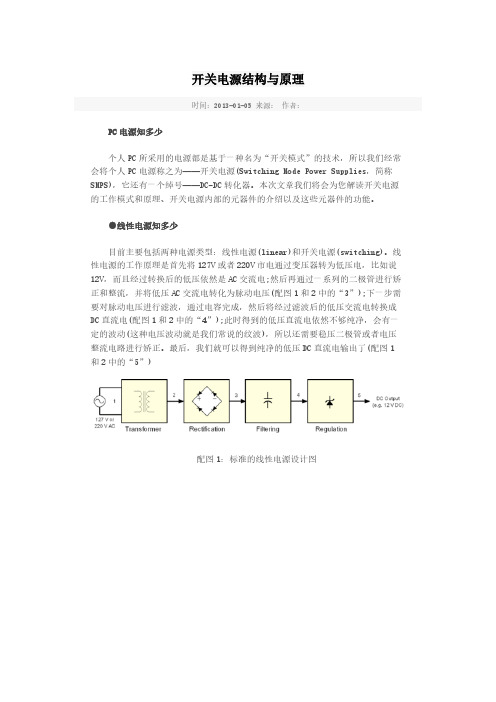
线性电源的工作原理是首先将127V或者220V市电通过变压器转为低压电,比如说12V,而且经过转换后的低压依然是AC交流电;然后再通过一系列的二极管进行矫正和整流,并将低压AC交流电转化为脉动电压(配图1和2中的“3”);下一步需要对脉动电压进行滤波,通过电容完成,然后将经过滤波后的低压交流电转换成DC直流电(配图1和2中的“4”);此时得到的低压直流电依然不够纯净,会有一定的波动(这种电压波动就是我们常说的纹波),所以还需要稳压二极管或者电压整流电路进行矫正。
最后,我们就可以得到纯净的低压DC直流电输出了(配图1和2中的“5”)配图1:标准的线性电源设计图配图2:线性电源的波形尽管说线性电源非常适合为低功耗设备供电,比如说无绳电话、PlayStation/ Wii/Xbox等游戏主机等等,但是对于高功耗设备而言,线性电源将会力不从心。
对于线性电源而言,其内部电容以及变压器的大小和AC市电的频率成反比:也即说如果输入市电的频率越低时,线性电源就需要越大的电容和变压器,反之亦然。
由于当前一直采用的是60Hz(有些国家是50Hz)频率的AC市电,这是一个相对较低的频率,所以其变压器以及电容的个头往往都相对比较大。
此外,AC市电的浪涌越大,线性电源的变压器的个头就越大。
由此可见,对于个人PC领域而言,制造一台线性电源将会是一件疯狂的举动,因为它的体积将会非常大、重量也会非常的重。

Selection GuidePart No.InputOutputFull LoadEfficiency (%)Typ.Max.Capacitive Load(µF)Voltage(VDC)(Range)Current(mA,Typ.)Full Load/No LoadVoltage (VDC)+Vo1/+Vo2Current (mA)+Io1/+Io2QA123HC-1504R312(10.8-13.2)215/8+15.0/-4.0+120/-12082/872200QA153HC-1504R315(13.5-16.5)171/82200QA243HC-1504R324(21.6-26.4)131/1077/822200QA123HC-2005R312(10.8-13.2)213/14+20.0/-5.0+90/-9082/87470QA153HC-2005R315(13.5-16.5)167/82200QA243HC-2005R324(21.6-26.4)129/1176/812200Input SpecificationsItemOperating ConditionsMin.Typ.Max.UnitInput Voltage (1sec.max.)Vin=12VDC DC -0.7--18VDC Vin=15VDC DC -0.7--21Vin=24VDCDC-0.7--30Input Filter Capacitance FilterHot PlugUnavailableOutput SpecificationsItem Operating ConditionsMin.Typ.Max.UnitOutput VoltageQA123HC-1504R3+Vo Vin=12VDC,Pin10&Pin9+Io=+120mA 14.2515.0015.75VDC -Vo Vin=12VDC,Pin9&Pin8-Io=-120mA -3.60-3.80-4.00QA153HC-1504R3+Vo Vin=15VDC,Pin10&Pin9+Io=+120mA 13.8014.5515.30-VoVin=15VDC,Pin9&Pin8-Io=-120mA-3.80-4.00-4.20DC-DC module power supply specialized for SIC driverRoHSFEATURES●High efficiency up to 87%●SIP package●I/O isolation test voltage:5.0kVAC(reinforced insulation )●Max.Capacitive Load:2200µF ●Ultra-low isolation capacitance●Operating ambient temperature range:-40℃to +105℃●Continuous short-circuit protection Industry standard pin-outQAxxxHC-R3is DC-DC module power supplie designed for SiC driver requiring two sets of isolation power supply.The mode of common ground outputs is adopted internally for better energy provision of SiC turn-on and turn-off.Output short-circuit protection and self-recovery capabilities are also provided.General application includes:1.Universal converter 2.AC servo drive system 3.Electric welding machine 4.Uninterruptible power supply (UPS)QA243HC-1504R3+Vo Vin=24VDC,Pin10&Pin9+Io=+120mA 14.5515.3016.05-Vo Vin=24VDC,Pin9&Pin8-Io=-120mA -3.96-4.16-4.36QA123HC-2005R3+Vo Vin=12VDC,Pin10&Pin9+Io=+90mA 18.6019.6020.60-Vo Vin=12VDC,Pin9&Pin8-Io=-90mA -4.95-5.20-5.45QA153HC-2005R3+Vo Vin=15VDC,Pin10&Pin9+Io=+90mA 18.4019.4020.40-Vo Vin=15VDC,Pin9&Pin8-Io=-90mA -4.85-5.10-5.35QA243HC-2005R3+Vo Vin=24VDC,Pin10&Pin9+Io=+90mA 19.0020.0021.00-VoVin=24VDC,Pin9&Pin8-Io=-90mA -4.75-5.00-5.25Voltage Accuracy 10%-100%load See output regulation curve (Fig.2)%Linear Regulation Full voltage input range+Vo Output --±1.1±1.5---Vo Output --±1.1±1.5Load Regulation 10%-100%load +Vo Output --815%-Vo Output--815Temperature Coefficient Full load--±0.04±0.1%/℃Ripple &Noise*20MHz bandwidth--50100mVp-pShort-circuit ProtectionContinuous,self-recoveryNote:*The “parallel cable”method is used for Ripple and Noise test,please refer to DC-DC Converter Application Notes for specific information.Mechanical SpecificationsCase Material Black plastic;flame-retardant and heat-resistant Dimensions 27.40x 9.50x 12.00mm Weight5.3g (Typ.)Cooling MethodFree air convectionElectromagnetic Compatibility (EMC)Emissions CE CISPR32/EN55032CLASS A (see Fig.7for recommended circuit)RE CISPR32/EN55032CLASS A (see Fig.7for recommended circuit)ImmunityESDIEC/EN61000-4-2Contact ±8kVperf.Criteria BGeneral SpecificationsItem Operating ConditionsMin.Typ.Max.Unit IsolationInput-output,Test for 1minute with a leakage current of 1mA max(reinforced insulation)5000----VAC Continuous insulation voltage(IEC61800-5-1)Input-output1700----V Insulation Resistance Input-output resistance at 500VDC 1000----M ΩIsolation capacitor Input-output capacitor at 100kHz/0.1V -- 3.55pF Electrical clearance Input-output 14.1414.74--mm Creepage distance Input-output 14.1414.74--mm CMTIInput-output±200----kV/usOperating Temperature Derating when operating temperature ≥85℃,(see Fig.1)-40--105℃Storage Temperature -55--125Pin Soldering Resistance TemperatureSoldering spot is 1.5mm away from case for 10seconds----300Case Temperature Rise Ta=25℃,nominal input voltage,full load ----40Storage Humidity Non-condensing5--95%RH Switching Frequency Full load,nominal input voltage --200--kHz MTBFMIL-HDBK-217F@25℃3500----k hoursTypical Characteristic CurvesFig.1Fig.2 Fig.3Note:Take QA153HC-2005R3as an example,other models can be corresponding referenceDesign Reference1.Over-load ProtectionThere is no over-load protection under normal operating conditions,we suggest to add an circuit breaker outside in the circuit.2.Test configurations12657VC3C1VinLoadDC/DC A VinGND +Vo 0V-VoFig.412765VC2C1LoadDC/DC A VinGND +Vo 0V-Vo Fig.5Note:C1,C2,C3:100µF/35V3.Typical applicationFig.6C1/C2/C3100µF/35V4.EMC typical recommended circuitFig.7LDM 33uHC1/C21.0µF/35V(Low internalresistance)5.Electrolytic capacitors are recommended for external capacitors at the input or output of the product.Tantalum capacitors are not,otherwise there is a risk of failure.6.The products do not support parallel connection of their output for power expansion purpose or hot-plug .7.For more information please find the application notes on SiC DriverControl SignalSiCDimensions and Recommended LayoutNotes:1.For additional information on Product Packaging please refer to .Packaging bag number:58200015;2.The lead wire connecting the power module and IGBT driver(or SiC MOSFET driver)should be as short as possible when in use;3.The output filter capacitor is as close as possible to the power module and IGBT driver(or SiC MOSFET driver);4.IGBT driver(or SiC MOSFET driver)gate drive current has a high peak value.5.It is recommended that the output filter capacitor of the power module use a low internal resistance electrolytic capacitor;6.The average output power of the driver must be lower than that of the power supply module;7.Consider fixing with glue near the module if being used in vibration occasion;8.The maximum capacitive load offered were tested at nominal input voltage and full load;9.Unless otherwise specified,parameters in this datasheet were measured under the conditions of Ta=25℃,humidity<75%RH with nominalinput voltage and rated output load;10.All index testing methods in this datasheet are based on company corporate standards;11.We can provide product customization service,please contact our technicians directly for specific information;12.Products are related to laws and regulations:see"Features"and"EMC";13.Our products shall be classified according to ISO14001and related environmental laws and regulations,and shall be handled byqualified units.MORNSUN Guangzhou Science&Technology Co.,Ltd.Address:No.5,Kehui St.1,Kehui Development Center,Science Ave.,Guangzhou Science City,Huangpu District,Guangzhou,P.R.China Tel:86-20-38601850Fax:86-20-38601272E-mail:***************。

PYBJ15-Q24-S5-Mdate 06/24/2019page1 of 9SERIES: PYBJ15 │ DESCRIPTION: DC-DC CONVERTERFEATURES• up to 15 W isolated output• ultra wide 4:1 input voltage range • single regulated output• output short circuit, over current, over voltage protection • efficiency up to 89%• DIP and SMT mounting styles • available with or without case• 1500 Vdc isolationMODELinput voltageoutput voltageoutput currentoutput powerripple & noise 1efficiency 2typ (Vdc)range (Vdc)(Vdc)min (mA)max (mA)max (W)max (mVp-p)typ (%)PYBJ15-Q24-S3249~36 3.30450014.8510088PYBJ15-Q24-S5249~365030001510088PYBJ15-Q24-S12249~3612012501510089PYBJ15-Q24-S15249~3615010001510089PYBJ15-Q48-S34818~75 3.30450014.8510088PYBJ15-Q48-S54818~755030001510088PYBJ15-Q48-S124818~7512012501510089PYBJ15-Q48-S154818~751510001510089Notes: 1. From 5~100% load, nominal input, 20 MHz bandwidth oscilloscope, with 10 µF tantalum and 1 µF ceramic capacitors on the output. From 0~5% load, ripple and noise is <5% Vo.2. Measured at nominal input voltage, full load.3. All specifications are measured at T a=25°C, humidity < 75%, nominal input voltage, and rated output load unless otherwise specified.PART NUMBER KEYBase NumberPYBJ15 - Q XX - S XX - X XInput VoltageOutput VoltageCase:“blank” = with case O = no caseMounting Style:D = DIPM = SMTdate 06/24/2019 │page 2 of 9 CUI Inc │ SERIES: PYBJ15 │DESCRIPTION: DC-DC CONVERTERINPUTparameter conditions/description min typ max unitsoperating input voltage24 Vdc input models48 Vdc input models 91824483675VdcVdcstart-up voltage24 Vdc input models48 Vdc input models 918VdcVdcsurge voltage24 Vdc input models for 1 second max48 Vdc input models for 1 second max -0.7-0.750100VdcVdcunder voltage shutdown24 Vdc input models48 Vdc input models 5.5126.515.5VdcVdccurrent 24 Vdc input models3, 5 Vdc output models12, 15 Vdc output models727718mAmA48 Vdc input models 3.3 Vdc output models5 Vdc output models363360mAmAstart-up current24 Vdc input models48 Vdc input models 3,0001,500mAmAremote on/off (CTRL)4turn on (CTRL pin pulled low to GND (0~1.2 Vdc))turn off (CTRL pin open or pulled high (3.5~12 Vdc))input current when switched off615mAalarm indication (ALM)Valm (relative to GND), when under voltage protection isgoing to happen, and during the over voltage protectionworking status.0.2 1.2Vdc Valm (relative to GND), other working status 3.59Vdcfilter Pi filterno load power consumption0.36W Notes: 4. The voltage of the CTRL pin is referenced to input GND pin.OUTPUTparameter conditions/description min typ max unitsmaximum capacitive load53.3, 5 Vdc output models12 Vdc output models15 Vdc output models4,7001,000820μFμFμFvoltage accuracy from 0% to full load±1±2% line regulation from low line to high line, full load±0.2±0.5% load regulation6from 5% to full load±0.5±1% switching frequency7PWM mode300kHz transient recovery time25% load step change, nominal input voltage300500μstransient response deviation 25% load step change, nominal input voltage3.3, 5 Vdc output modelsall other output models±3±3±8±5%%temperature coefficient at full load±0.03%/°C Note: 5. Tested at input voltage range and full load.6. At 0~100% load, the max load regulation is ±3%.7. Value is based on full load. At loads <50%, the switching frequency decreases with decreasing load for efficiency improvement.date 06/24/2019 │ page 3 of 9CUI Inc │ SERIES: PYBJ15 │ DESCRIPTION: DC-DC CONVERTER PROTECTIONSparameterconditions/description min typmax units over voltage protection output shut down 110160%over current protection hiccup, auto recovery110180230%short circuit protectionhiccup, continuous, auto recoverySAFETY AND COMPLIANCEparameter conditions/descriptionmin typ max units isolation voltageinput to output for 1 minute at 1 mA input to case 8 for 1 minute at 1 mA output to case 8 for 1 minute at 1 mA 1,500500500Vdc Vdc Vdc isolation resistance input to output at 500 Vdc input to case 8 at 500 Vdc output to case 8 at 500 Vdc 100100100MΩMΩMΩisolation capacitance input to output, 100 kHz / 0.1 V 1,000pFsafety approvals IEC 62368-1, EN 62368-1conducted emissions CISPR32/EN55032, class B (external circuit required, see Figure 2-a) radiated emissions CISPR32/EN55032, class B (external circuit required, see Figure 2-a)ESDIEC/EN61000-4-2, contact ±6 kV , class B radiated immunity IEC/EN61000-4-3, 10 V/m, class AEFT/burst IEC/EN61000-4-4, ±2 kV , class B (external circuit required, see Figure 2-b)surgeIEC/EN61000-4-5, line-line ±2 kV , class B (external circuit required, see Figure Figure 2-b)conducted immunity IEC/EN61000-4-6, 3 Vr .m.s, class A MTBF as per MIL-HDBK-217F , 25°C 1,000,000hoursRoHSyesNote:8. Only applies to versions with case.ENVIRONMENTALparameterconditions/description min typmax units operating temperature see derating curves-4085°C storage temperature -55125°C storage humidity non-condensing595%vibration10~150 Hz, for 60 minutes on each axis 5GDERATING CURVESO u t p u t L o a d (%)60801004020120 0Temperature Derating Curve(Output Load vs. Ambient Tempearature3.3, 5 Vdc output models)O u t p u t L o a d (%)60801004020120 070Temperature Derating Curve(Output Load vs. Ambient Tempearature12, 15 Vdc output models)date 06/24/2019 │ page 4 of 9CUI Inc │ SERIES: PYBJ15 │ DESCRIPTION: DC-DC CONVERTER MECHANICALparameterconditions/descriptionmintypmaxunits dimensionsDIP without case:3.3, 5 Vdc output models: 38.70 x 27.20 x 6.20 [1.524 x 1.071 x 0.244 inch]12, 15 Vdc output models: 38.70 x 27.20 x 5.80 [1.524 x 1.071 x 0.228 inch]mm mm DIP with case:3.3, 5 Vdc output models: 39.10 x 29.50 x 6.80 [1.539 x 1.161 x 0.268 inch]12, 15 Vdc output models: 39.10 x 29.50 x 6.40 [1.539 x 1.161 x 0.252 inch]mm mm SMT without case:3.3, 5 Vdc output models: 38.70 x 27.20 x 6.20 [1.524 x 1.071 x 0.244 inch]12, 15 Vdc output models: 38.70 x 27.20 x 5.80 [1.524 x 1.071 x 0.228 inch]mm mm SMT with case:3.3, 5 Vdc output models: 39.10 x 29.50 x 6.80 [1.539 x 1.161 x 0.268 inch]12, 15 Vdc output models: 39.10 x 29.50 x 6.40 [1.539 x 1.161 x 0.252 inch]mm mm case material aluminum alloyweightwithout case 3.3, 5 Vdc output models without case 12, 15 Vdc output models with case 3.3, 5 Vdc output models with case 12, 15 Vdc output models11.08.813.811.5g g g g10 Sec. Max.Wave Soldering Time4 Sec. Max.Peak Temp. 260°C Max.Time (sec.)T e m p e r a t u r e (°C )25020015010050SOLDERABILITYparameter conditions/descriptionmin typ max units hand soldering 1.5 mm from case for 10 seconds 300°C wave soldering 9see wave soldering profile260°C reflow soldering 10see reflow soldering profileMaximum duration >217°C is 60 seconds.For actual application, refer to IPC/JEDEC J-STD-020D.1245°CNote: 9. For DIP models only. 10. For SMT models only.50100150200250245217T e m p e r a t u r e (°C )Time (sec.)60 sec max (>217°C)Peak Temp 245°CWave Soldering Proflile(DIP models)Reflow Soldering Profile(SMT models)date 06/24/2019 │ page 5 of 9CUI Inc │ SERIES: PYBJ15 │ DESCRIPTION:DC-DC CONVERTER units: mm [inch]tolerance: ±0.50[±0.020]pin section tolerance: ±0.10[±0.004]Recommended PCB LayoutTop Viewunits: mm [inch]tolerance: ±0.50[±0.020]pin section tolerance: ±0.10[±0.004]MECHANICAL DRAWING (DIP WITH CASE )Recommended PCB LayoutTop ViewMECHANICAL DRAWING (DIP WITHOUT CASE )PIN CONNECTIONS PIN Function 1+Vo 2+Vo 3+Vo 40V 50V 6NC 7ALM 8CTRL 9NC 10+Vin 11+Vin 12GND 13GND PIN CONNECTIONS PIN Function 1+Vo 2+Vo 3+Vo 40V 50V 6NC 7ALM 8CTRL 9NC 10+Vin 11+Vin 12GND 13GND 14NCNote: NC = no connectdate 06/24/2019 │ page 6 of 9CUI Inc │ SERIES: PYBJ15 │ DESCRIPTION: DC-DC CONVERTER units: mm [inch]tolerance: ±0.50[±0.020]pin section tolerance: ±0.10[±0.004]MECHANICAL DRAWING (SMT WITHOUT CASE )Recommended PCB LayoutTop Viewunits: mm [inch]tolerance: ±0.50[±0.020]pin section tolerance: ±0.10[±0.004]MECHANICAL DRAWING (SMT WITH CASE )PIN CONNECTIONS PIN Function 1+Vo 2+Vo 3+Vo 40V 50V 6NC 7NC 8ALM 9CTRL 10NC 11+Vin 12+Vin 13GND 14GND Recommended PCB LayoutTop ViewPIN CONNECTIONS PIN Function 1+Vo 2+Vo 3+Vo 40V 50V 6NC 7NC 8ALM 9CTRL 10NC 11+Vin 12+Vin 13GND 14GND 15NCNote: NC = no connectdate 06/24/2019 │page 7 of 9 CUI Inc │ SERIES: PYBJ15 │DESCRIPTION: DC-DC CONVERTERAPPLICATION CIRCUITFigure 1 Table 1Vin+Vo0V Vout(Vdc)Cin(μF)Cout(μF)3.3/5/12/1510010This series has been tested according to the following recommended circuit (Figure 1) before leaving the factory. If you want to further reduce the input and output ripple, you can increase the input and output capacitors or select capacitors of low equivalent impedance provided that the capacitance is less than the maximum capacitive load of the model.EMC RECOMMENDED CIRCUITTable 2Figure 2Recommended External Circuit ComponentsVin (Vdc)2448FUSE choose according to actual input currentC0470 µF / 50 V680 µF / 100 VC1, C2 4.7 µF / 50 V 4.7 µF / 100 VC3refer to the Cout in T able 1C4330 µF / 50 V330 µF / 100 VLCM1 4.7 µHCY1, CY22000 pF /2 kVdate 06/24/2019 │page 8 of 9 CUI Inc │ SERIES: PYBJ15 │DESCRIPTION: DC-DC CONVERTERPACKAGINGunits: mmInner Carton Size: 280 x 196 x 63 mmOuter Carton Size: 600 x 285 x 225 mmOuter Carton QTY: 288 pcsdate 06/24/2019 │ page 9 of 9CUI Inc │ SERIES: PYBJ15 │ DESCRIPTION: DC-DC CONVERTER CUI offers a two (2) year limited warranty. Complete warranty information is listed on our website.Headquarters20050 SW 112th Ave.Tualatin, OR 97062800.275.4899Fax 503.612.2383cui .com*******************rev.description date 1.0initial release06/24/2019The revision history provided is for informational purposes only and is believed to be accurate.REVISION HISTORYPYBJ15-Q24-S5-M。
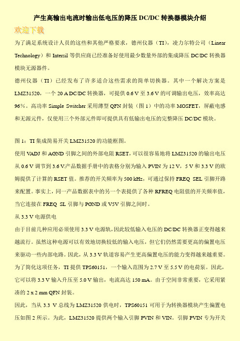
产生高输出电流时输出低电压的降压DC/DC转换器模块介绍为了满足系统设计人员的这些和其他严格要求,德州仪器(TI),凌力尔特公司(Linear Technology)和Intersil等供应商已经准备好使用最少数量外部的集成降压DC/DC转换器模块无源器件。
德州仪器(TI)已经发布了许多适合这些需求的简单切换器。
其中一个解决方案是LMZ31520,一个20 A DC/DC转换器,可提供0.6 V至3.6 V的可调输出电压,效率高达96%。
高功率Simple Switcher采用薄型QFN封装(图1)中的功率MOSFET,屏蔽电感和无源元件,仅使用三个外部元件即可提供具有低输出电压的完整降压DC/DC模块。
图1:TI集成简易开关LMZ31520的功能框图。
使用V ADJ和AGND引脚之间的外部电阻RSET,可以很容易地将LMZ31520的输出电压从0.6 V调节到3.6 V.产品数据手册中的表格分别为输入PVIN为12 V,5 V和3.3 V的欧姆提供了计算的RSET值。
推荐的开关频率为500 kHz,可通过保持FREQ_SEL引脚开路来配置。
事实上,同一产品数据表中的另一个表提供了各种RFREQ电阻值的开关频率值,当它连接在FREQ_SL引脚与PGND或V5V引脚之间时。
从3.3 V电源供电由于目前几种应用必须使用3.3 V电源轨,因此较低输入电压的DC/DC转换器正变得越来越流行。
虽然这种电源可以有效地切换较低的输入电压,但它们仍然需要更高的偏置电压来驱动一些内部电路。
因此,从3.3 V轨道容易产生更高偏置电压的能力变得越来越重要。
为了简化这项任务,TI提供TPS60151,一个输入范围为2.7 V至5.5 V的电荷泵。
因此,它可以将3.3 V输入升压至5.0 V输出,电流高达150 mA。
由于空间非常重要,它采用紧凑的2 x 2 mm QFN封装。
因此,当从3.3 V总线为LMZ31520供电时,TPS60151可用于为转换器模块产生偏置电压如图2所示。

凌力尔特公司推出具有集成输出断接功能的DC转换器
佚名
【期刊名称】《电信技术》
【年(卷),期】2012(000)010
【摘要】2012年10月18日,凌力尔特公司推出具有集成输出断接功能的
3MHz电流模式、同步升压型DC/DC转换器LTC3122。
其内部2.5A开关在
启动时的18~5.5V(运行时为05V)输入电压范围内提供高达15V的输出电压,从而使该器件非常适用于电池或标准33V和5V电源。
LTC3122从5V输入转换
至12V时能提供高达800mA的连续输出电流。
【总页数】1页(P82-82)
【正文语种】中文
【中图分类】TN492
【相关文献】
1.凌特推出具有输出断接功能的1.4A,1.5MHz同步升压型DC/DC转换器 [J],
2.凌力尔特推出具集成输出断接功能的转换器 [J],
3.凌力尔特推出双通道DC/DC转换器用于有源矩阵OLED和CCD偏置的升压型和负输出DC/DC转换器 [J],
4.凌力尔特推出具动态可调输出的3通道同步降压型DC/DC转换器 [J],
5.凌力尔特公司推出新型3A输出、2MHz同步降压-升压型DC/DC转换器 [J],因版权原因,仅展示原文概要,查看原文内容请购买。
Intersil推出高效4通道直流/直流转换器
无
【期刊名称】《电子测试:新电子》
【年(卷),期】2005(000)010
【摘要】Intersil公司目前宣布推出高效4通道直流/直流转换器,可用于电视或桌面监视器等的大屏(19英寸或更大)TFT—LCD(薄膜晶体管液晶显示器)。
EL7585A具有集成3.5AFET(场效应晶体管),可为大型显示屏提供高输出功率。
它还具有极高的电源效率,引入了冷却运行系统,通过提高集成度缩小印制电路设计的面积。
【总页数】1页(P100)
【作者】无
【作者单位】无
【正文语种】中文
【中图分类】TN873.93
【相关文献】
1.美国国家半导体推出多款无需加设电感器的全新高效率降压直流/直流转换器,进一步扩大便携式系统电源管理芯片系列的产品阵容 [J],
2.NS推出面向便携式应用的4MHz同步降压直流/直流转换器 [J], 无
3.美国国家半导体推出面向便携式应用的最小型1A、4MHz同步降压直流/直流转换器 [J],
4.IR推出性能卓越的高温高压直流一直流转换器 [J],
5.Intersil推出业界最大集成3.5AFET的高效直流/直流转换器 [J],
因版权原因,仅展示原文概要,查看原文内容请购买。
Intersil推出高性能同步降压DC—DC转换器
佚名
【期刊名称】《中国集成电路》
【年(卷),期】2009(18)6
【摘要】Intersil公司宣布,推出高性能同步降压DC—DC转换器ZL2008,带有引脚设置(pin—strap)补偿和电流分配功能。
ZL2008发挥了Zilker Labs专利的Digital-DCTM技术优势,专为数字式电源模块而设计,使系统设计师能够轻松对板级电源进行配置,时刻领先于市场需求的变化。
【总页数】1页(P5-5)
【关键词】同步降压;转换器;DC;性能;Intersil公司;电源模块;电流分配;Labs
【正文语种】中文
【中图分类】TP335;TM42
【相关文献】
1.Intersil推出AEC-Q100认证的汽车等级高性能双通道同步降压DC/DC稳压器[J],
2.Intersil推出AEC-Q100认证的汽车等级高性能双信道同步降压DC/DC稳压器[J],
3.高性能同步降压DC/DC转换器 [J],
4.凌力尔特推出具双输入电源通路控制的同步降压-升压型DC/DC转换器 [J],
5.Linear推出1.5A同步降压型DC/DC转换器,2MHz提供93%效率 [J],
因版权原因,仅展示原文概要,查看原文内容请购买。