PSRR
- 格式:pdf
- 大小:116.62 KB
- 文档页数:8
音频放大器PSRR测量技术及其电源纹波效应探讨,由于免除不必要的数字模拟转换,因此可降低成本,并提升性能。
但是,如今市场上的封闭回路I2S 放大器并不普遍,因为要建立反馈回路来进行PWM 输出取样并且与内送I2S 数字音频串流(digital audio stream) 相加总是相当困难的。
在模拟反馈系统中,通常是模拟输出与模拟输入相加总,因此较为简易可行。
然而,随着I2S 市场的演变,大多数的I2S 放大器都采取模拟输入放大器的做法,并采用反馈架构。
显然PSRR 不是测量BTL D 类放大器供电抑制的有效方法,那么应该怎么做?现在回头谈谈互调这个名词。
设计人员需要测量在播放音频时所产生的互调失真及其对应的THD+N 配置。
在开始之前,让我们先回顾一下SE 架构。
在SE 架构中,不论是AB 类、D 类或Z 类,都没有BTL 架构的抵消作用,这是因为喇叭的其中一端连接放大器,另一端则接地。
因此,对于AB 类或D 类放大器而言,在SE 架构中,传统的PSRR 测量都能够确实指出供电噪音抑制的情形。
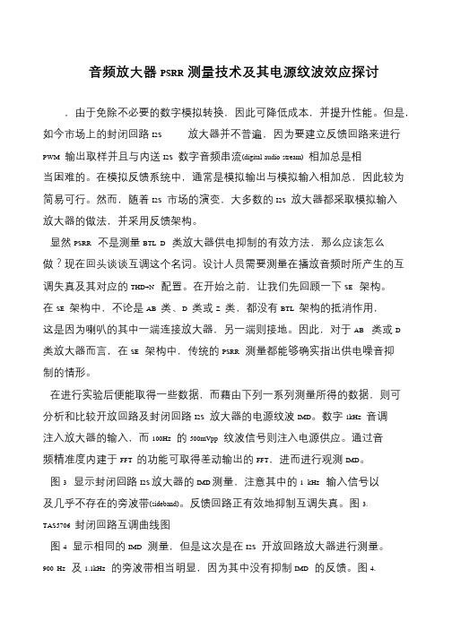
在进行实验后便能取得一些数据,而藉由下列一系列测量所得的数据,则可分析和比较开放回路及封闭回路I2S 放大器的电源纹波IMD。
数字1kHz 音调注入放大器的输入,而100Hz 的500mVpp 纹波信号则注入电源供应。
通过音频精准度内建于FFT 的功能可取得差动输出的FFT,进而进行观测IMD。
图3 显示封闭回路I2S 放大器的IMD 测量,注意其中的1 kHz 输入信号以及几乎不存在的旁波带(sideband)。
反馈回路正有效地抑制互调失真。
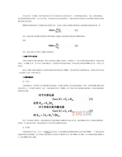
图3. TAS5706 封闭回路互调曲线图图4 显示相同的IMD 测量,但是这次是在I2S 开放回路放大器进行测量。
900 Hz 及1.1kHz 的旁波带相当明显,因为其中没有抑制IMD 的反馈。
图4.。
在实际应用一个电路时,噪声和波动常会在不知不觉时被引入到供电电压中,从而影响输出端电压。
为此,要使电路稳定,就必须消除或抑制这些噪声。
基于这个原因,弄清楚由供电电压导致的噪声,在输出端是如何表现的以及如何测量并削弱这些影响输出的噪声是必要的。
PSRR是电路抑制来自于电源噪声能力的量化术语。
它被定义为输入端到输出端的增益与电源到输出端增益的比值,即这里,A(s)=输入端到输出端的增益=Gm×Rout;Ap(s)=电源到输出端的增益=GMp×Rout。
因此这里,Gm为输入信号跨导;GMp为电源跨导。
1 改善PSRR的方法为减小电源波动对输出端的影响,Gm必须增加而GMp必须减小。
理想情况下,要完全排除电源波动的影响,就要使Gm 无限大,而GMp为0。
文中介绍了共源共栅技术,负反馈技术和采用附加电路。
3种改善放大器电路PSRR的方法,并进行了仿真验证。
通过从VDD到输出端能够反方向影响电源波动的负增益改善PSRR,从而反映到放大电路的输出端。
共源放大器为应用这一技术提供了支撑,结果已被证实。
2 共源共栅技术2.1 简介共源共栅技术,尽管增加了放大器的输出阻抗Rout,却也极大地增加了放大器电路的增益。
然而,从电源VDD到输出端的增益仍然为1,与共源放大器相同。
这样,共源共栅技术改善了PSRR,由于它增加了输入端到输出端的增益,而保持电源到输出端的增益为常数。
然而,和共源放大器相比,共源共栅也带来了输出摆幅和3 dB频率点减小的不足。
输出摆幅减小是由于Vd输出摆幅值要求较低。
由于输出能力增加,输出端的频率点左移而导致3 dB频率的减小。
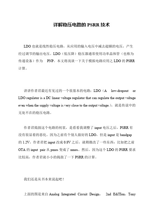
2.2 电路共源电路如图1所示,它由一个P MOS管作为负载,以负载MOS管的偏置电路来估计放大器的PSRR。
一个30 μA的电流源被用做放大器的偏置。
这个共源放大器的增益可以仿真到3 dB频率为5.43 MHz8寸的356。
由于电源端的增益AVDD为1,因此PSRR仍然为356。
详解稳压电路的PSRR技术
LDO也就是线性稳压电路,从应用的输入电压中减去超额的电压,产生经过调节的输出电压。
LDO(低压降)稳压器通常使用功率晶体管(也称为传递设备)作为PNP。
本文将浅谈一下关于模拟电路应用之LDO的PSRR 计算。
讲讲作者君最近有见过的一个很基本的电路:LDO(A low-dropout or LDO regulator is a DC linear voltage regulator that can regulate the output voltage even when the supply voltage is very close to the output voltage.),就是传说中的无处不在的稳压电路。
作者君捣鼓这个电路的初衷,是看看我调整了input电压之后,PSRR有没有很显着的恶化。
因为之前有个别人做好的LDO,但是input是bandgap
的1.2V,作者君把input改成0.8V之后,就稍微改了一些东西:比如把之前OTA的input pair从pmos变成了nmos。
然后,因为这个LDO的PSRR要求比较高,作者君就小小的捣鼓了一下PSRR的计算。
我们还是从书本来说起吧!
上面的图是来自Analog Integrated Circuit Design,2nd EdiTIon,Tony。
PSRR参数一、PSRR参数概述PSRR(Peak Signal-to-Noise Ratio)参数是一种用于评估音频处理系统性能的重要参数,它表示音频信号峰值与背景噪声之间的比率。
PSRR通过对音频信号的峰值进行测量,并比较这些峰值与背景噪声的均方根值,以提供一种量化音频质量的手段。
二、PSRR参数的计算方法PSRR参数的计算公式为:PSRR(dB) = 20 * log10(Vpeak / Vnoise),其中Vpeak表示处理后音频信号的最大值,Vnoise表示背景噪声的均方根值。
在计算PSRR时,通常采用快速傅里叶变换(FFT)等技术对音频信号进行频谱分析,以获取信号的最大值和噪声的均方根值。
三、PSRR参数在音频处理系统中的应用PSRR参数在音频处理系统的许多方面都得到了广泛的应用。
首先,PSRR可以用于评估音频压缩算法的性能。
通过测量压缩前后音频信号的PSRR值,可以量化压缩算法对音频质量的影响。
其次,PSRR可用于音频去噪算法的评价。
通过对添加噪声前后的音频信号进行PSRR计算,可以评估去噪算法的有效性。
此外,PSRR还广泛应用于音频编解码器性能评估、音频质量检测等领域。
四、PSRR参数与其他性能指标的关系PSRR参数与音频处理系统中的其他性能指标密切相关。
例如,较高的PSRR 值通常意味着更好的音频质量,而较低的PSRR值则可能表明音频质量较差。
此外,PSRR参数与信噪比(SNR)和音质损失指数(QLI)等其他性能指标之间存在一定的关系。
深入理解这些关系可以帮助我们更好地评估和比较各种音频处理系统的性能。
五、PSRR参数的优缺点分析PSRR参数的优点在于其简单易计算,能够快速评估音频信号的质量。
此外,PSRR参数对峰值信号的变化非常敏感,因此能够准确地反映音频信号中的噪声和失真。
然而,PSRR参数也存在一些局限性。
例如,它对背景噪声的均方根值进行测量,可能无法充分反映人耳对不同频率噪声的感知差异。
PSRR--电源抑制比(Power Supply Rejection Ratio):把电源的输入与输出看做独立的信号源,输入与输出的纹波比值即是PSRR,通经常使用对数形式表示,单位是dB。
PSRR=20log{[ripple(in)/ripple(out)]}关于高质量的D/A转换器,要求开关电路及运算放大器所用的电源电压发生转变时,对输出的电压阻碍极小.CMRR--共模抑制比,英文全称是Common Mode Rejection Ratio,因此一样用简写CMRR来表示。
为了说明差动放大电路抑制共模信号的能力,经常使用共模抑制比作为一项技术指标来衡量,其概念为放大器对差模信号的电压放大倍数Aud与对共模信号的电压放大倍数Auc 之比. 差模信号电压放大倍数Aud越大,共模信号电压放大倍数Auc越小,那么CMRR 越大。
现在差分放大电路抑制共模信号的能力越强,放大器的性能越好。
当差动放大电路完全对称时,共模信号电压放大倍数Auc=0,那么共模抑制比CCMR→∞,这是理想情形,事实上电路完全对称是不存在的,共模抑制比也不可能趋于无穷大。
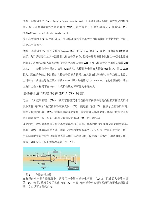
降低电话的"嗡嗡"噪声(RF 217Hz 噪音)电话、个人数字助理(PDA) 和其它便携式通信设备常常在条件恶劣而且噪声相当大的环境下工作。
这推动了新式音频功率放大器(PA) 的进展,这些PA 提供了全差动的架构,实现了良好的射频(RF)、共模和电源纹波抑制。
本文将讨论单端架构、典型桥接负载和全差动的音频放大器,另外还将探讨噪声对电源和RF 校正的阻碍。
业界利用三种要紧类型的音频功率放大器架构:单端、典型的桥接负载和全差动的放大器。
单端(SE) 音频功率放大器一样是所有架构中最简单的一种。
只是,在电话中咱们一样不用其驱动酷炫铃声或免提操作模式等应用的扬声器。
SE 放大器一样都用于驱动耳机,用于欣赏MP3格式的音乐或游戏音频(图1)。
图1 单端音频功放在典型的单电源单端配置中,需要用一个输出耦合电容器(COUT) 阻止放大器输出处的DC 偏置,这就幸免了负载中的DC 电流。

电源抑制比定义电源抑制比(Power Supply Rejection Ratio,简称PSRR)是电子电路中一个重要的性能参数,它用来衡量电路对电源电压变化的抑制能力。
PSRR的定义是电源电压变化引起电路输出电压变化的比例,通常以分贝(dB)为单位来表示。
理想的电路应该具有无限大的PSRR,即电源电压的变化不会引起输出电压的任何变化。
以下是对电源抑制比定义的详细介绍。
一、电源抑制比的定义电源抑制比(PSRR)定义为电源电压变化引起电路输出电压变化的比例。
当电源电压发生变化时,电路的输出电压也会相应发生变化,PSRR衡量的是这种变化的程度。
二、电源抑制比的单位电源抑制比通常以分贝(dB)为单位来表示。
分贝是一个对数单位,用于表示两个物理量之间的比例关系。
在电源抑制比的定义中,分贝用来表示电源电压变化与输出电压变化之间的比例关系。
三、电源抑制比的意义1. 电源抑制比反映了电路对电源电压变化的敏感程度。
一个高的PSRR值意味着电路对电源电压的变化不敏感,即电路能够有效地抑制电源电压的变化。
2. 电源抑制比是评估电路稳定性的重要指标。
一个高的PSRR值表明电路在电源电压变化时能够保持输出电压的稳定,这对于许多应用来说是非常重要的。
3. 电源抑制比对于电路的设计和优化具有指导意义。
通过提高PSRR值,可以设计出更加稳定和鲁棒的电路。
四、影响电源抑制比的因素1. 电路的设计:电路的设计决定了其对电源电压变化的敏感程度。
合理的设计可以提高PSRR值。
2. 元器件的选择:元器件的特性也会影响电源抑制比。
例如,选择具有高PSRR值的运放可以改善整个电路的PSRR。
3. 电源电压的稳定性:电源电压的稳定性也会影响电路的PSRR。
一个稳定的电源电压可以降低电路的PSRR值。
4. 电路的负载:电路的负载也会影响电源抑制比。
不同的负载条件下,电路的PSRR值可能会有所不同。
五、提高电源抑制比的方法1. 选择具有高PSRR值的元器件:在电路设计中,选择具有高PSRR值的运放、稳压器等元器件可以提高整个电路的PSRR。
什么是PSRR以及影响它的变量有哪些?
低压差线性稳压器(LDO)最大的优点之一是它们能够衰减开关模式电
源产生的电压纹波。
这对锁相环(PLL)和时钟等信号调节器件在内的数据
转换器尤为重要,因为噪声电源电压会影响性能。
我的同事Xavier Ramus在博客中介绍了噪音对信号调节设备的不利影响:减少高速信号链电源问题。
然而,电源抑制比(PSRR)仍然通常被误认为单一的静态值。
在这篇文章中,我将尝试说明什幺是PSRR以及影响它的变量有哪些。
什幺是PSRR?
PSRR是许多LDO数据手册中的公共技术要求。
它规定了某个频率的AC 元件从输入到LDO输出的衰减程度。
公式1表示PSRR为:
该等式告诉您衰减越高,每分贝的PSRR值越高。
(应该指出的是,一些
供应商会使用负号来表示衰减。
大多数供应商,包括德州仪器都不这样用。
)
在数据手册的电气特性表中找到频率为120Hz或1kHz的PSRR并不罕见。
但是,单独使用此规范可能对确定指定LDO是否符合您的过滤要求没有多大帮助。
让我们来看看为什幺这幺说。
psrr 共模增益
PSRR(电源抑制比)和共模增益是电子和电气工程中用于描述电路性能的两个重要参数,尤其在处理模拟信号时。
PSRR,全称为电源抑制比,是一个用于描述电源电压变化对电路输出信号影响程度的参数。
在许多电子应用中,电源电压的波动可能会影响到电路的性能。
PSRR就是用来量化这种影响的。
一个高的PSRR值意味着电源电压的变化对电路输出的影响较小,从而有助于提高信号的稳定性。
而共模增益则是描述电路对共模信号的放大能力的参数。
共模信号是在电路的两个输入端同时出现的信号,通常是由外部噪声或者其他干扰源产生的。
共模增益可以帮助我们了解电路对这种信号的放大程度。
一个适当的共模增益可以帮助电路更好地抑制外部噪声,从而提高信号的信噪比。
在实际应用中,高的PSRR和低的共模增益通常被认为是理想的。
高的PSRR可以减少电源电压波动对电路性能的影响,而低的共模增益则有助于减少外部噪声的干扰。
然而,这两个参数往往是一对矛盾:提高PSRR可能会牺牲共模增益的性能,反之亦然。
因此,在设计和优化电路时,工程师需要在这两者之间做出权衡,以满足特定应用的需求。
总的来说,PSRR和共模增益是衡量电子电路性能的重要参数,对于理解电路性能和优化设计至关重要。
PSRR介绍Understanding power supply ripple rejection in linear regulatorsPower supply ripple rejection ratio (PSRR) is a measure of how well a circuit rejects ripple coming from the input power supply at various frequencies and is very critical in many RF and wireless applications. In the case of an LDO,it is a measure of the output ripple compared to the input ripple over a wide frequency range (10 Hz to 10 MHz is common) and is expressed in decibels (dB). The basic equation for PSRR isMore specifically, PSRR for an LDO can be written aswhere A V is the open-loop gain of the regulator feedback loop, and A VO is the gain from V IN to V OUT with the regula-tor feedback loop open. From this equation it can be seenPSRR AA V VO =20log ,PSRR Ripple Ripple InputOutput =20log .that to increase the PSRR it is beneficial to increase the open-loop gain and decrease the gain from V IN to V OUT.Typically, A VO is significantly less than 0 dB, with –10 to –15 dB being typical; this is entirely driven by internal and external parasitics from input to output and at the gate of the pass FET. Figure 1 shows a simplified regulator block diagram with a PMOS pass device.Another parameter that is closely related to PSRR is line transient response. PSRR is specified at specific frequencies,whereas a line transient essentially contains all frequencies due to the Fourier components of a step function. However,the primary difference is that PSRR is based on small signals, whereas line transients are large signals and thus theoretically much more complicated in nature. Sinceimproving PSRR typically improves line transient response and vice versa, all of the effects on PSRR discussed in this article will usually have a similar effect on the line tran-sient response.Texas Instruments IncorporatedPower Management By John C. Teel (Email: jteel@/doc/757b3488680203d8ce2f2498.html )Analog IC Designer, Member Group Technical StaffTexas Instruments Incorporated Power ManagementA curve showing PSRR over a wide frequency range is shown in Figure 2.As mentioned previously, the open-loop gain of the LDO feedback circuit is the dominant factor in PSRR (at least in a limited frequency range); therefore, LDOs requiring good PSRR typically have high gain with a high unity-gain frequency (large gain-bandwidth product). However, this makes the loop more difficult to stabilize, which limits how much the gain-bandwidth product can be increased to improve PSRR. It is important to have a high unity-gain frequency so that the amplifier does not lose open-loop gain at relatively low frequencies, causing PSRR to roll off also.The curve in Figure 2 shows that PSRR for an LDO can be broken down into three basic frequency regions.Region 1 is from dc to the roll-off frequency of thebandgap filter and is dominated by both open-loop gain and bandgap PSRR. Region 2 extends from the bandgap filter roll-off frequency up to the unity-gain frequency where PSRR is dominated mainly by the open-loop gain of the regulator. Region 3 is above the unity-gain frequency,where the feedback loop has very little effect, so the out-put capacitor dominates along with any parasitics from V IN to V OUT . The gate driver’s ability to drive the pass-FET gate at high frequencies also has an effect in Region 3. A larger output capacitor with less equivalent series resistance (ESR) will typically improve PSRR in this region, but it can also actually decrease the PSRR at some frequencies.This is because increasing the output capacitor lowers the unity-gain frequency, causing the open-loop gain to roll off earlier and thus lowering PSRR. Nevertheless, the minimum PSRR that occurs at the unity-gain frequency will typically be improved.Anything affecting the gain of the feedback loop also affects PSRR in Region 2. One example is load current. As load current increases, the open-loop output impedance of the LDO decreases (since a MOSFET’s output impedance is inversely proportional to the drain current), thus lower-ing the gain. Increasing the load current also pushes the output pole to higher frequencies, which increases the feedback loop bandwidth.The net effect of increasing the load is therefore reduced PSRR at lower frequencies(because of the reduced gain) along with increased PSRR at higher frequencies.The differential dc voltage between input and output is another example of how a change in the feedback loop gain also affects PSRR. As V IN –V OUT is lowered to less than about 1 V, the internal pass FET (which provides gain in a PMOS design) starts to be pushed out of the active (satura-tion)region of operation and into the triode/linear region,which causes the feedback loop to lose gain. The dividing line between the active region and the triode region is proportional to the square root of the drain (load) current.So as the load current is increased, the voltage across the device (V IN –V OUT ) necessary to keep it in the active region increases as a function of the square root of the load cur-rent. For example, having V IN –V OUT at only 0.5 V may have no negative effect on PSRR at light load currents because the pass FET device doesn’t need much headroom to stay in the active region and to preserve gain. At heavier loads,Texas Instruments IncorporatedPower Managementhowever, 0.5 V may no longer be sufficient and the pass FET device may enter the triode region, causing the circuit to lose gain, thus reducing PSRR. When PSRR is compared among various LDOs, it’s important always to compare LDOs with identical V IN –V OUT and I Load conditions. It’s also important to compare LDOs with identical output voltages,since PSRR is usually better at lower output voltages.One of the dominant internal sources of PSRR in an LDO is the bandgap reference. Any ripple that makes its way onto the reference will be amplified and sent to the output, so it’s important to have a bandgap reference with high PSRR. Typically, the solution is simply to filter the bandgap with a low-pass filter (LPF). This LPF is almost always accomplished with a large internal resistor and an external capacitor. The effect of the LPF can be seen in Region 1 of Figure 2, where the PSRR is somewhat reduced because the LPF passes bandgap ripple in this frequency range.As has been shown, there are many ways to improve the PSRR in an LDO application. The most important is to start with a low-noise, high-PSRR LDO designed for high-PSRR applications such as one from the TPS793/4/5/6xx family or the low-I q TPS799xx family. The next most important way is to choose a low-ESR ceramic outputcapacitor and to determine the capacitance value based on the frequencies at which PSRR is most important. Finally,board layout must be carefully done to reduce the feedthrough from input to output via board parasitics.Related Web sites/doc/757b3488680203d8ce2f2498.html/doc/757b3488680203d8ce2f2498.html /sc/device/partnumberReplace partnumber with TPS79301, TPS79401,TPS79501, TPS79601, or TPS79901IMPORTANT NOTICETexas Instruments Incorporated and its subsidiaries (TI) reserve the right to make corrections, modifications, enhancements, improvements, and other changes to its products and services at any time and to discontinue any product or service without notice. Customers should obtain the latest relevant information before placing orders and should verify that such information is current and complete. All products are sold subject to TI's terms and conditions of sale supplied at the time of order acknowledgment. TI warrants performance of its hardware products to the specifications applicable at the time of sale in accordance with TI's standard warranty. Testing and other quality control techniques are used to the extent TI deems necessary to support this warranty. Except where mandated by government requirements, testing of all parameters of each product is not necessarily performed.TI assumes no liability for applications assistance or customer product design. Customers are responsible for their products and applications using TI components. To minimize the risks associated with customer products and applications, customers should provide adequate design and operating safeguards.TI does not warrant or represent that any license, either express or implied, is granted under any TI patent right, copyright, mask work right, or other TI intellectual property right relating to any combination, machine, or process in which TI products or services are used. Information published by TI regarding third-party products or services does not constitute a license from TI to use such products or services or a warranty or endorsement thereof. Use of such information may require a license from a third party under the patents or other intellectual property of the third party, or a license from TI under the patents or other intellectual property of TI. Reproduction of information in TI data books or data sheets is permissible only if reproduction is without alteration and is accompanied by all associated warranties, conditions, limitations, and notices. Reproduction of this information with alteration is an unfair and deceptive business practice. TI is not responsible or liable for such altered documentation.Resale of TI products or services with statements different from or beyond the parameters stated by TI for that product or service voids all express and any implied warranties for the associated TI product or service and is an unfair and deceptive business practice. TI is not responsible or liable for any such statements. Following are URLs where you can obtain information on other Texas Instruments products and application solutions: TI Worldwide Technical Support InternetTI Semiconductor Product Information Center Home Page/doc/757b3488680203d8ce2f2498.htmlTI Semiconductor KnowledgeBase Home Page/doc/757b3488680203d8ce2f2498.html /sc/knowledgebaseProduct Information CentersAmericasPhone+1(972) 644-5580Fax+1(972) 927-6377 Internet/Email /doc/757b3488680203d8ce2f2498.html /sc/pic/americas.htmEurope, Middle East, and AfricaPhoneBelgium (English)+32 (0) 27 45 54 32Netherlands (English)+31 (0) 546 87 95 45 Finland (English)+358 (0) 9 25173948Russia+7 (0) 95 7850415 France+33 (0) 1 30 70 11 64Spain+34 902 35 40 28 Germany+49 (0) 8161 80 3311Sweden (English)+46 (0) 8587 555 22 Israel (English)1800 949 0107United Kingdom+44 (0) 1604 66 33 99 Italy800 79 11 37Fax+(49) (0) 8161 80 2045Internet /doc/757b3488680203d8ce2f2498.html /sc/pic/euro.htmJapanFaxInternational+81-3-3344-5317Domestic0120-81-0036 Internet/EmailInternational /doc/757b3488680203d8ce2f2498.html /sc/pic/japan.htmDomestic www.tij.co.jp/picAsiaPhoneInternational+886-2-23786800Domestic Toll-Free Number Toll-Free Number Australia1-800-999-084New Zealand0800-446-934China800-820-8682Philippines1-800-765-7404 Hong Kong800-96-5941Singapore800-886-1028Indonesia001-803-8861-1006Taiwan0800-006800Korea080-551-2804Thailand001-800-886-0010 Malaysia1-800-80-3973Fax886-2-2378-6808Email tiasia@/doc/757b3488680203d8ce2f2498.html Internet/doc/757b3488680203d8ce2f2498.html /sc/pic/asia.htm ti-china@/doc/757b3488680203d8ce2f2498.htmlC011905 Safe Harbor Statement:This publication may contain forward-looking statements that involve a number of risks and uncertainties. These “forward-looking statements” are intended to qualify for the safe harbor from liability established by the Private Securities Litigation Reform Act of 1995. These forward-looking statements generally can be identified by phrases such as TI or its management “believes,” “expects,” “anticipates,”“foresees,” “forecasts,” “estimates” or other words or phrases of similar import. Similarly, such statements herein that describe the company's products, business strategy, outlook, objectives, plans, intentions or goals also are forward-looking statements. All such forward-looking statements are subject to certain risks and uncertainties that could cause actual results to differ materially from those in forward-looking statements. Please refer to TI's most recent Form 10-K for more information on the risks and uncertainties that could materially affect future results of operations. We disclaim any intention or obligation to update any forward-looking statements as a result of developments occurring after the date of this publication.Trademarks: All trademarks are the property of theirrespective owners.Mailing Address: Texas InstrumentsPost Office Box 655303Dallas, Texas 752652005 Texas Instruments IncorporatedSLYT202。