FC722芯片使用手册
- 格式:pdf
- 大小:399.48 KB
- 文档页数:7
12378910目录欢迎您加入日益兴旺的新型INFINITI英菲尼迪车主的行列。
我们满怀信心地向您提供该新型INFINITI英菲尼迪汽车。
它是用最新技术并在严格的质量管理下制造的。
本使用说明手册是为您了解车辆的操作和保养而准备的,有了它,您可享受久驶不损之乐趣。
在使用本车之前,请通读本手册。
另附的《保修和保养手册》对车辆的保修进行了详细的说明。
INFINITI英菲尼迪经销店最了解您汽车的情况。
如果您需要什么服务或有任何问题,我们都会运用重要的安全信息安全注意事项!遵守下列重要的驾驶规则,可确保您和乘客旅途的安全!.切勿酒后或服药后驾驶。
.务必观察限速标志,切勿超速驾驶。
.务必使用安全带及恰当的儿童保护装置。
未满13岁的儿童应坐在后座。
.务必提醒乘客车辆安全装置的正确使用方法。
.务必查阅本使用说明手册以获取重要的安全信息。
本手册说明本手册包括了有关该车型所有选装件的资料。
因此您可能会发现其中有些资料并不适用于您的车辆。
本手册中的所有资料,包括规格和插图,在本手册出版时有效。
INFINITI英菲尼迪汽车公司保留在任何时候修改车辆的规格或设计的权利,恕不另行通知。
车辆的改装不应对该车辆进行改装。
改装可能会影响车辆的性能、安全性或耐久性,甚至可能会违反政府的法规。
另外,INFINITI英菲尼迪汽车公司提供的保修服务将不包括由于改装所引起的损坏或性能问题。
请先阅读—然后安全驾驶在驾驶车辆之前,请仔细阅读本用户手册。
这能确保您熟悉车辆的控制与保养要求,有助于您安全驾驶。
在本手册中,我们使用了符号伴随警告二字。
这表示有可能导致死亡或严重人身伤害的危险。
要避免或降低这种风险,必须认真遵守操作程序。
在本手册里还使用符号伴随注意二字来表示有可能引起轻微或中度人身伤害或车辆损害的危险。
要避免或降低这种风险,必须认真遵守操作程序。
SIC0697如果您看到此符号,它表示“请勿进行此操作”或“请勿让此情况发生”。
如果您在插图中看到与此类似的符号,它表示箭头指向车头。
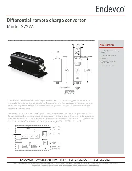
Differential remote charge converter Model 2777AKey features• Acceleration and velocityoutputs• 4-wire output device• Low noise• Frequency response(10 Hz - 10 kHz)• Two optional gainsModel 2777A-XX-YY Differential Remote Charge Convertor (DRCC) is a low noise ruggedized device designedfor use with differential piezoelectric transducers. This device converts the transducer’s high impedance chargeinput to a low impedance voltage output. The acceleration output is also integrated to produce an AC voltageproportional to velocity output.The low impedance output from the DRCC provides less susceptibility to noise in the cabling from the DRCC tothe main signal conditioning instrument, and it also makes the system’s noise level insensitive to the capacitanceof the cable connecting the DRCC to the main conditioner. This is a low noise device with a frequency response of10 Hz to 10 kHz. The DRCC operates over the temperature range of 5°F to 185°F (-15°C to 85°C).DifferentialInputVelocityOutAccelOut+Verify-Verify22-31 VDC PIN BPIN CPIN DPIN FPIN EOUTPUTINPUTGround PIN ADifferential remote charge converterModel 2777ASpecificationsInputsDifferential PE inputInput connection Differential with shield connected to caseInput source resistance 50 KΩ minimumInput source capacitance 30 000 pF, maximumMaximum input charge 37 500 pC pkOutputsAcceleration and velocity (Output is single ended)Output impedance 50 Ω maximumCapacitance load 30 000 pF maximumDC output bias (DC offset) 9.0 Vdc ±1.5 Vdc over the temp range 5˚F to 185˚F (-15˚C to 85˚C)Linear output voltage 10 Vpk-pk minimumLimited output voltage 15 Vpk-pk with 22 Vdc minimum compliance voltageOuput current 15 mA maximumLinearity ±1% of reading from the best straight lineResidual noise (RTO) -02-YYY: 1.0 mV RMS maximum, -10-YYY: 5mV RMS maximum referred to output Transfer characteristicsGain (Cs = 1000 pf) -02-YYY:2 mV/EU per pC/g,-10-YYY:10mV/EU per pC/g(for acceleration: EU=g) (for velocity: EU=IPS)Gain error ±3.0% at 100 Hz for Cs< 1000 pF (at 25˚C)Gain stability with temperature Less than ±1%Frequency response Flat within the lower and upper cutoff frequenciesLower cutoff frequency Acceleration: High-pass-roll-off -36 dB/octave at f < 2.27 Hz(Reference frequency 100Hz) Velocity: High-pass roll-off -42 dB/octave at f < 2.27 Hz-5% corner frequency YYY = 10/15/20/25/150 Hz ±10%-3 dB Corner frequency = 5.73/8.59/11.5/14.3/86 Hz ±10%Upper cutoff frequency Low-pass roll-off -12 dB/octave(Reference frequency 100 Hz) -5% corner = 10 kHz ±5%, -3dB corner = 17.5 kHz ±10%Power requirementsDC voltage requirements 22 Vdc to 31 VdcDC current requirement 15 mAWarm up time 10 secPhysical characteristicsDimensions 1.72” h x 1.67” w x 5.5” d (46.5 mm x 42.4 mm x 139.77mm)Weight 8.0 oz maximumCase material AluminumFinish Black powder coat, fine texture using Cardinal P141-BK03 or equiv Environmental characteristicsOperating temperature 5°F to 185°F (-15°C to 85°C)Short term operating temperature -10°F to 185°F (-23.3°C to 85°C)Storage temperature -76°F to 257°F (-60°C to 125°C)Humidity The unit will withstand 95% relative humidityVibration 7 g-pk from 55 Hz to 2 kHzShock 100 g-pk with 3.6 ms haver-sine pulseRadiation 105 Rads (integrated Gamma)Reliability (MTBF) 30 000 hours or greaterDifferential remote charge converter Model 2777AContactENDEVCO T el: +1 (866) ENDEVCO [+1 (866) 363-3826]Notes:1. Maintain high levels of precision and accuracy using Endevco’s factory calibration services. Call Endevco’s inside sales force at 866-ENDEVCO for recommended intervals, pricing and turn-around time for these services as well as for quotations on our standard products.AccessoriesOrdering informationWhere YYY is 10, 15, 20, 25 or 150 Hz lower cut-off frequency。

目录1. 远程控制概述 (1)1.1 如何远程控制 (1)1.2 通信协议 (3)1.3 远程控制功能 (5)2. SCPI简介 (10)2.1 命令格式 (10)2.2 符号说明 (10)2.3 参数类型 (11)2.4 命令缩写 (12)3. 模式共用命令 (13)3.1 IEEE公用命令子系统 (13)3.2 系统命令 (15)3.3 存储命令 (20)3.4 显示控制 (21)3.5 模式命令 (22)3.6 扫描命令 (22)4. 频谱分析模式 (24)4.1 仪器模式命令 (24)4.2 Initiate命令子系统 (24)4.3 Sense命令子系统 (25)4.4 Calculate命令系统 (43)4.5 Measurement命令系统 (58)4.6 触发 (72)4.7 TG (73)4.8 调制解调 (75)5. 矢量网络分析模式 (77)5.1 频率控制 (77)5.2 幅度控制 (78)5.3 带宽控制 (80)5.4 扫描控制 (80)5.5 TG (81)5.6 迹线 (81)5.7 光标 (85)6. 故障定点分析模式 (98)6.1 频率控制 (98)6.2 幅度控制 (99)6.3 扫描控制 (100)6.4 迹线 (101)6.5 光标 (102)6.6 测量 (105)7. 调制分析模式 (110)7.1 频率控制 (110)7.2 幅度控制 (111)7.3 带宽控制 (112)7.4 扫描控制 (113)7.5 迹线 (114)7.6 光标 (117)7.7 测量 (119)7.8 触发 (124)8. 实时频谱分析模式 (126)8.1 频率控制 (126)8.2 幅度控制 (129)8.3 带宽控制 (131)8.4 扫描控制 (132)8.5 迹线 (134)8.6 光标 (137)8.7 触发 (139)8.8 测量 (142)9. EMI测量 (145)9.1 频率控制 (145)9.2 幅度控制 (147)9.3 带宽控制 (150)9.4 扫描控制 (151)9.5 迹线 (153)9.6 光标 (155)9.7 限制 (159)10. 编程示例 (168)10.1 使用VISA的编程示例 (168)10.2Sockets/Telnet示例 (182)SIGLENT 1. 远程控制概述分析仪支持通过USB、LAN、GPIB-USB接口与计算机进行通信。
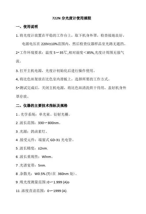
722N分光度计使用规程一、使用说明1.将光度计放置在平稳的工作台上,取下机身外罩,检查接地良好,电源电压在220V±10%范围内,然后检查仪器样品室光路无遮挡。
2•工作环境要求:温度5〜35℃,相对湿度<85%,光度计周围无强气流。
3.打开主机电源,光度计初始化后进行操作使用。
4,将比色皿架放在比色室内滑板上,选择所要的工作方式。
5•测试完成后,关闭主机电源,将比色皿清洗烘干待用,盖好机身外罩存放。
二、仪器的主要技术指标及规格1.光学系统:单光束、衍射光栅。
2.波长范围:330〜800nm。
3.光源:鸽卤素灯。
4.接受元件:端窗式GD-31光电管。
5.波长精度:±2nm.6.波长重现性:Wlnm。
7.光谱宽带:5nm.8.杂散光:W0.5% (T)(在360nm 处)。
9.吸光度测量范围:0〜1.999 (A)o11.浓度直读范围:0〜1999 (A).12.光度精度:A.透光度线性精度±0.5% (T).B.吸光度精度±0.004A(在0.5A处)。
13.透光度重现性0.5% (T).三、仪器的使用方法1.使用仪器前,使用者应该首先了解本仪器的结构和工作原理,以及各个操作旋钮的功能。
在未接通电源前,应对仪器进行检查, 电源线接线应牢固,通地要良好,各个调节旋钮的起始位置要正确,然后接通电源开关。
2.开启电源,指示灯亮,选择开关置于“T” ,波长调至测试用波长。
仪器预热30分钟。
3.打开试样室盖,调节“0”旋钮,使数字显示为"0.00"盖上试样室盖,将比色皿架处于蒸储水校正位置,使光电管受光,调节透过率“100%”旋钮,使数字显示为“100.0”4.预热后,按(3)连续几次调整“0”和“100%”,仪器即可进行测定工作。
5.吸光度的测量:按(3)调整仪器的“00.0”和“100%”后,将选择开关置于,调节吸光度调零旋钮,使数字显示为".000",然后将被测样品移入光路,显示值即为被测样品的吸光度值。
数控车床LBR-370-e操作使用说明书出版号: LC722-002-V7J un.2016OKUMA-BYJC在使用本机之前,请充分掌握本说明书的内容,进行正确的操作或作业。
如有疑问之处,请与本公司经销商或售后服务部进行联络。
重要说明1. 务必遵守本说明书内的安全注意事项,以及贴在机械上的安全铭牌的内容。
如果没有遵从这些内容,可能会造成重大的人身事故或物品损害。
如果需要交换用的安全铭牌,请向本公司订购。
2. 为说明细节部分,本说明书中部分例图以卸下护罩或门的状态画出。
请注意,为安全起见,在实际运转时必须装好。
3. 切忌擅自进行影响机械安全性的任何改造。
如需要改造,请与本公司经销商或售后服务部联络。
4. 机械出现故障时与本公司经销商或售后服务部进行联络,切忌擅自拆解维修,因拆解维修不当所引起的任何后果应由责任方承担。
5. 请将本使用说明书保管在机械附近,以便随时查阅。
安全注意事项本机床配有很多安全装置,用它们来防止由于意外事故造成人身的伤害和机床本身的损坏。
但是操作人员的误操作还可能导致严重的意外事故。
为了避免发生意外事故,在操作机床之前,应该通读本操作使用说明书,全面了解本机床的功能。
本操作使用说明书和固定在机床外罩上的警告标志只是指出了北一大隈公司可以预见到的危险,并非全部危险内容。
1.机床搬运、安装中的注意事项(1)机床搬运方法有两种:一种是采用随机附属的吊钩吊装;另一种是垫辊子牵引。
在操作时请注意下列各项。
吊装注意事项a.请使用直径超过¢20的钢丝绳。
b.请注意吊起前钢丝绳在不接触机床情况下的吊装角度。
(单根钢丝绳与垂直方向的夹角不要超过40°)c.请平稳水平吊起。
d.机床放下时要缓慢下降,以防下降速度快而撞击地面。
机床大概重量(约kg)1ST × 250 4,000kg 1SC × 500 4,200kg- -1SC ×1000 5,900kg(机床重量中包含油压单元、电柜、NC装置的重量。

I N S T A L L A T I O N I N S T R U C T I O N SMedium/Large Side-by-Side Accessoryfor Carts and StandsDutch Product DescriptionMAC722 / PAC722MAC722 / PAC722Installation Instructions2DISCLAIMERMilestone AV Technologies and its affiliated corporations and subsidiaries (collectively "Milestone"), intend to make thismanual accurate and complete. However, Milestone makes no claim that the information contained herein covers all details,conditions or variations, nor does it provide for every possible contingency in connection with the installation or use of this product. The information contained in this document is subject to change without notice or obligation of any kind. Milestone makes no representation of warranty, expressed or implied,regarding the information contained herein. Milestone assumes no responsibility for accuracy, completeness or sufficiency of the information contained in this document.Chief® is a registered trademark of Milestone AV Technologies.All rights reserved.IMPORTANT WARNINGS AND CAUTIONS!WARNING: A WARNING alerts you to the possibility ofserious injury or death if you do not follow the instructions.CAUTION: A CAUTION alerts you to the possibility ofdamage or destruction of equipment if you do not follow the corresponding instructions.WARNING:Failure to read, thoroughly understand, andfollow all instructions can result in serious personal injury,damage to equipment, or voiding of factory warranty! It is the installer’s responsibility to make sure all components are properly assembled and installed using the instructions provided.WARNING:Failure to provide adequate structural strengthfor this component can result in serious personal injury or damage to equipment! It is the installer’s responsibility to make sure the structure to which this component is attached can support five times the combined weight of all equipment.Reinforce the structure as required before installing the component. The wall to which the mount is being attached may have a maximum drywall thickness of 5/8" (1.6cm).WARNING:Exceeding the weight capacity can result inserious personal injury or damage to equipment! It is the installer’s responsibility to make sure the combined weight of all components located on the accessory does not exceed 150 lbs (68.0 kg) [75 lbs (34.0) per faceplate].LEGENDApretar elemento de fijación Befestigungsteil festziehen Apertar fixador Serrare il fissaggio Bevestiging vastdraaien Serrez les fixations Aflojar elemento de fijación Befestigungsteil lösen Desapertar fixador Allentare il fissaggio Bevestiging losdraaien Desserrez les fixationsLlave de cabeza hexagonal Sechskantschlüssel Chave de cabeça sextavada Chiave esagonale Zeskantsleutel Clé à tête hexagonale Llave de boca Gabelschlüssel Chave de bocas Chiave a punte aperte Steeksleutel Clé à fourcheInstallation Instructions MAC722 / PAC722 DIMENSIONS3MAC722 / PAC722Installation Instructions TOOLS REQUIRED FOR INSTALLATIONPARTS4Installation Instructions MAC722 / PAC722Assembly and InstallationThe MAC722 and PAC722 side-by-side accessories are for usewith Chief carts and stands.3.Attach faceplates (B and C)OR(D and E) to the extensionassembly (A) using two 5/16-18 x 3-1/2" button head capscrews (F) and two 5/16" locking nuts (G) for eachfaceplate. (See Figure 3)6WARNING:CART/STAND OR DISPLAY FALLING CAUSING SERIOUS PERSONAL INJURY OR DAMAGE TO EQUIPMENT!Extension measurement MUST be the same for both sides of the MAC722/PAC722.Attaching DisplaysWARNING:MAY LEAD TO SERIOUS PERSONAL INJURY ORDAMAGE TO EQUIPMENT! It is the installer’s responsibility to ensure the total amount of weight placed on the MAC722/PAC722 does not exceed 150 lbs (68.0 kg) [75 lbs (34.0) per faceplate].WARNING:PAC722 ensure the stand or cart is on a level surface.CAUTION:MAC722/PAC722 is evenly distributed.CAUTION:adjusting the height of the stand or cart.1.Adjust the stand or cart to the desired height by slightly lifting the inner column, pulling out knob on the center post and turning 90mechanism. (See Figure 6)2.Raise or lower the center post, then turn the knob 90direction to engage the knob and lock the stand at desired height. (See Figure 6)3.Attach interface brackets to the displays following the instructions included with the bracket.4.While supporting both sides of display, align four mounting buttons on display or interface bracket with four mounting holes in head assembly. (See Figures 10 and 11)(PAC722 shown)Two holes for full extensionInner ColumnWARNING:40 LBS! Always use two people and proper lifting techniques when installing or positioning display on stand.5.Lower display into place listening for audible "click" toensure recessed area of mounting buttons are properlyseated in lower area of mounting holes.(See Figure 7) and (See Figure 8)WARNING:STAND OR DISPLAY FALLING CAUSING SERIOUS PERSONAL INJURY OR DAMAGE TO EQUIPMENT! Ensure mounting buttons are completely engaged in mounting holes.NOTE:the pin and nut may be removed from the upper holesand moved to the lower holes for use as a morepermanent locking device. (See Figure 8)Figure 8Tilting DisplayThe display(s) can be tilted up to 5o either backward or forward from a straight upright position.1.Turn knob counterclockwise on back of faceplate to loosenthe tilt. (See Figure 9)Figure 92.Tilt display as desired, to a maximum of 5o either forward orbackward.3.Turn knob clockwise to tighten display on head assembly.(See Figure 9)CAUTION:Tighten knob on back of faceplate to prevent damage to the stand or cart.4.If leaving the display in a straight upright position, it isrecommended that a bolt (not provided) be placed through the faceplate (See Figure 9) to lock the display into theupright position.5.Repeat Steps 1-4 for remaining faceplate and display. Cable Management1.The display power cords can be run through the front of theextension assembly (A). (See Figure 4)2.The cords can then run through the extension assembly tothe center of the assembly. (See Figure 4)3.When the cords are run to the center of the extensionassembly, they can either exit out the front, or down through the cart or stand column. (See Figure 4)4.Any accessory power cords can be run through the frontFigure 10Remove pinand nut andmove to lower holes7MAC722 / PAC722Installation InstructionsUSA/InternationalA 8401 Eagle Creek Parkway, Savage, MN 55378P 800.582.6480 / 952.894.6280F 877.894.6918 / 952.894.6918EuropeA Fellenoord 130 5611 ZB EINDHOVEN, The Netherlands P +31 (0)40 2668620F +31 (0)40 2668615Asia PacificARoom 24F, Block D, Lily YinDu International BuildingLuoGang, BuJi Town, Shenzhen, CHINA.P +86-755-8996 9226F +86-755-8996 9217Chief Manufacturing, a products division of Milestone AV Technologies 8807-002006 Rev002009 Milestone AV Technologies, a Duchossois Group Company 06/09。
BL0972交/直流电能计量芯片数据手册V1.0目录1、产品简述 (5)2、基本特征 (6)2.1主要特点 (6)2.2系统框图 (7)2.3管脚排列(TSSOP20) (7)2.4性能指标 (8)2.4.1电参数性能指标 (8)2.4.2极限范围 (9)3、工作原理 (10)3.1电流电压波形产生原理 (10)3.1.1PGA增益调整 (10)3.1.2相位补偿 (11)3.1.3通道偏置校正 (11)3.1.4通道增益校正 (12)3.1.5电流电压波形输出 (12)3.2有功功率计算原理 (13)3.2.1有功波形的选择 (14)3.2.2有功功率输出 (14)3.2.3有功功率校准 (14)3.2.4有功功率的防潜动 (15)3.2.5有功功率小信号补偿 (15)3.3有功能量计量原理 (16)3.3.1有功能量输出 (16)3.3.2有功能量输出选择 (16)3.3.3有功能量输出比例 (17)3.4电流电压有效值计算原理 (17)3.4.1有效值输出 (18)3.4.2有效值输入信号的设置 (18)3.4.3有效值刷新率的设置 (18)3.4.4电流电压有效值校准 (19)3.4.5有效值的防潜动 (19)3.5快速有效值检测原理 (20)3.5.1快速有效值输出 (20)3.5.2快速有效值输入选择 (21)3.5.3快速有效值累计时间和阈值 (21)3.5.4电网频率选择 (21)3.5.5快速有效值超限数据保存 (22)3.5.6过流指示 (22)3.5.7继电器控制 (22)3.6温度计量 (23)3.7.1线周期计量 (23)3.7.2线频率计量 (23)3.7.3相角计算 (24)3.7.4功率符号位 (24)3.8故障检测 (25)3.8.1过零检测 (25)3.8.2峰值超限 (25)3.8.3线电压跌落 (26)3.8.4过零超时 (27)3.8.5电源供电指示 (28)4、内部寄存器 (30)4.1电参量寄存器(只读) (30)4.2校表寄存器(外部写) (30)4.3OTP寄存器 (32)4.4模式寄存器 (33)4.4.1 MODE1寄存器 (33)4.4.2 MODE2寄存器 (33)4.4.3 MODE3寄存器 (34)4.5中断状态寄存器 (34)4.5.1 STATUS1寄存器 (34)4.5.2 STATUS3寄存器 (34)4.6校表寄存器详细说明 (34)4.6.1 通道PGA增益调整寄存器 (34)4.6.2 相位校正寄存器 (35)4.6.3 有效值增益调整寄存器 (35)4.6.4 有效值偏置校正寄存器 (36)4.6.5 有功小信号补偿寄存器 (36)4.6.7 防潜动阈值寄存器 (36)4.6.8 快速有效值相关设置寄存器 (37)4.6.9 过流报警及控制 (38)4.6.11 能量读后清零设置寄存器 (39)4.6.12 用户写保护设置寄存器 (39)4.6.13 软复位寄存器 (39)4.6.14 通道增益调整寄存器 (40)4.6.15 通道偏置调整寄存器 (40)4.6.16 有功功率增益调整寄存器 (40)4.6.17 有功功率偏置调整寄存器 (41)4.6.20 CF缩放比例寄存器 (41)4.7电参数寄存器详细说明 (42)4.7.1 波形寄存器 (42)4.7.2 有效值寄存器 (42)4.7.3 快速有效值寄存器 (42)4.7.7 电能脉冲计数寄存器 (43)4.7.8 波形夹角寄存器 (44)4.7.9 快速有效值保持寄存器 (44)4.7.11 线电压频率寄存器 (44)5、SPI通讯接口 (45)5.1概述 (45)5.2工作模式 (45)5.3帧结构 (45)5.4读出操作时序 (46)5.5写入操作时序 (47)5.6SPI接口的容错机制 (48)6、典型应用图 (49)7、封装信息 (50)1、产品简述BL0972是一颗内置时钟的单相交/直流电能计量芯片。
产品概述FM7222DS是高精度原边反馈的LED恒流驱动芯片。
芯片工作在电感电流断续模式,适用于85Vac~265Vac全范围输入电压、反激式隔离LED恒流电源。
FM7222DS芯片内部集成650V功率开关,采用原边反馈模式,无需次级反馈电路,也无需补偿电路,只需要极少的外围元件即可实现恒流。
采用专利的驱动和电流检测方式,芯片的工作电流极低,无需变压器辅助绕组检测和供电,进一步减少外围元器件,极大的节约了系统成本和体积。
FM7222DS芯片内带有高精度的电流取样电路,使得LED输出电流精度达到±5%以内。
芯片采用了特有的恒流控制方式,可以达到优异的线性调整率。
FM7222DS具有多重保护功能,包括LED开路/短路保护,欠压保护,芯片过温保护等。
特性➢内部集成650V功率管;➢原边反馈恒流控制,无需次级反馈电路;➢无需变压器辅助绕组检测和供电;➢芯片超低工作电流;➢宽输入电压;➢±5% LED 输出电流精度;➢LED短路/开路保护;➢芯片供电欠压保护;➢过温保护;➢封装形式:SOP-8 。
应用范围➢LED射灯;➢LED 球泡灯;➢其它LED照明。
内部框图流和交流电参数规范。
对于未给定上下限值的参数,该规范不予保证其精度,但其典型值合理反映了器件性能。
注2:温度升高最大功耗一定会减小,这也是由TJMAX, θJA,和环境温度TA所决定的。
最大允许功耗为PDMAX (TJMAX - TA)/ θJA或是极限范围给出的数字中比较低的那个值。
推荐工作范围电气特性应用信息FM7222DS是一款专用于LED照明的恒流驱动芯片,采用专有的恒流架构和控制方法,芯片内部集成650V功率开关,只需要极少的外围组件就可以达到优异的恒流特性。
采用了原边反馈技术,FM7222DS无需光耦及TL431反馈,也无需辅助绕组供电和检测,系统成本极低。
启动系统上电后,母线电压通过启动电阻对V CC电容充电,当V CC电压达到芯片开启阈值时,芯片内部控制电路开始工作。

DSC2210FM2-A0030Crystal-less™ Configurable Clock GeneratorGeneral DescriptionThe DSC2210FM2-A0030 is a programmable, high performance LVCMOS oscillators utilizing Microchip's proven silicon MEMS technology to provide excellent jitter and stability while incorporating additional device functionality.The DSC2210FM2-A0030 allows the user to easily modify the frequency using SPI interface.The user can also select from two pre-programmed default output frequencies using the frequency select pin.Applications• Consumer Electronics • Storage Area Networks- SATA, SAS, Fibre Channel • Passive Optical Networks- EPON, 10G-EPON, GPON, 10G-GPON • Ethernet- 1G, 10GBASE-T/KR/LR/SR, and FCoE • HD/SD/SDI Video & Surveillance • PCI Express • AutomotiveFeatures• Frequency and output formats:- LVCMOS 50/25MHz• Low RMS phase jitter: <1ps (typ)• ±25ppm frequency stability• -55°C to +125°C automotive temperature range • High supply noise rejection: -50dBc • SPI programmable frequency and drive • Excellent shock & vibration immunity - Qualified to MIL-STD-883• High reliability- 20x better MTF than quartz oscillators • Supply range of 2.25 to 3.6V • AEC-Q100 automotive qualified• 14-pin 3.2mm x 2.5mm QFN packageBlock DiagramControl CircuitryMEMS PLL VSSVDD/VDD2÷ 2÷ M1CLK150MHz LVCMOSOEFS ClockWorks is a registered trademark of Microchip Technology Inc.Microchip Technology Inc.October 31, 2019Revision 1.0*********************8418Ordering InformationOrdering Part Number Industrial Temperature RangeShippingPackageDSC2210FM2-A0030-55°C to +125°C Tube 14-pin 3.2mm x 2.5mm QFN DSC2210FM2-A0030T-55°C to +125°CTape and Reel14-pin 3.2mm x 2.5mm QFNDevices are Green and RoHS compliant. Sample material may have only a partial top mark.Pin Configuration14-pin 3.2mm x 2.5mm QFNOE NC SCLK GNDNC NC NC CLK1M O S IM I S OS S _b a rV D D 2V D DF SPin DescriptionPin NumberPin Name Pin TypePin Function1OE IEnables outputs when high and disables outputs when low 2NC Leave unconnected or connect to ground 3SCLK I SPI serial clock from master to slave 4GND PWR Ground5MOSI SPI serial data from master to slave 6MISO O SPI serial data from slave to master 7SS_bar SPI slave select (active low)8CLK1O LVCMOS output9NC Leave unconnected or connect to ground 10NC Leave unconnected or connect to ground 11NC Leave unconnected or connect to ground 12, 13VDD2, VDDPWR Power supply14FSI Frequency select pin, see Table 2 for detailsOctober 31, 20192Revision 1.0*********************8418Operational DescriptionThe DSC2210FM2-A0030 is a LVCMOS oscillator consisting of a MEMS resonator and a supportingPLL IC. The LVCMOS output is generated through independent 8-bit programmable dividers from the output of the internal PLL.DSC2210FM2-A0030 allows for easy programming of the output frequencies using SPI interface. Uponpower-up, the initial output frequency is controlledby an internal pre-programmed memory (OTP). This memory stores all coefficients required by the PLLfor two different default frequencies. The control pin (FS) selects the initial frequency. Once the device is powered up, a new output frequency can be programmed. Programming details are provided in the Programming Guide.When OE (pin 1) is floated or connected to VDD, the DSC2210FM2-A0030 is in operational mode. Driving OE to ground will disable both output drivers (hi-impedance mode).DSC2210FM2-A0030 has programmable output drive strength, which can be controlled via SPI.Table 1 displays typical rise / fall times for the output with a 15pF load capacitance as a function of these control bits at VDD = 3.3V and room temperature.Output Drive Strength Bits [OS2, OS1, OS0] - Default is [111]000001010011100101110111 tr (ns) 2.1 1.7 1.6 1.4 1.3 1.3 1.2 1.1 tf (ns) 2.5 2.4 2.42 1.8 1.6 1.3 1.3Table 1. Rise/Fall Times for Drive StrengthsOutput Clock FrequenciesFrequency select bits are weakly tied high so if left unconnected the default setting will be [1] and the device will output the associated frequency highlighted in bold.Freq (MHz)Freq Select Bit [FS] - Default is [1]01CLK12550Table 2. Pin-Selectable Output FrequenciesAbsolute Maximum RatingsItem Min.Max.Units Condition Supply Voltage-0.3+4.0VInput Voltage-0.3VDD + 0.3VJunction Temp-+150°CStorage Temp-55+150°CSoldering Temp-+260°C40sec max. ESDHBM MM CDM -40004001500V1000+ years of data retention on internal memoryOctober 31, 20193Revision 1.0********************* 8418Specifications (Unless specified otherwise: T = 25°C, max LVCMOS drive strength)44Parameter Symbol ConditionMin.Typ.Max.Units Supply Voltage¹VDD 2.253.6V Supply Current IDD OE pin low - output is disabled2123mA Frequency Stability F Includes frequency variation due to initial tolerance, temp. and power supply voltage ±25ppm Aging F First year (@ 25°C)±5ppm Startup Time²tSU T = 25°C5ms Input Logic Levels Input Logic High Input Logic Low VIH VIL 0.75 x VDD--0.25 x VDDV Output Disable Time³tDA 5ns Output Enable Time³tEN20ns Pull-Up Resistor Pull-up exists on all digital IO40kOhmsLVCMOS OutputSupply Current IDDOE pin high - output is enabled CL = 15pF, F0 = 125MHz 3135mAOutput Logic Levels Output Logic High Output Logic Low VOH VOL I = ±6mA0.9 x VDD--0.1 x VDDVOutput Transition Time³ Rise Time Fall Time tR tF 20% to 80%CL = 15pF 1.11.322ns Frequency CLK1[FS] = [1]50MHz Output Duty Cycle SYM 4555%Period JitterJPER F0 = 125MHz3psRMSIntegrated Phase NoiseJPH200kHz to 20MHz @ 125MHz 100kHz to 20MHz @ 125MHz 12kHz to 20MHz @ 125MHz0.30.381.72psRMSNotes:1. Pin 12 VDD2, and pin 13 VDD should be filtered with 0.1uF capacitors.2. tSU is time to 100ppm stable output frequency after VDD is applied and outputs are enabled.3. Output Waveform and Test Circuit figures below define the parameters.4. Output is enabled if OE pin is floated or not connected.October 31, 20194Revision 1.0*********************8418Nominal Performance Parameters(Unless specified otherwise: T = 25°C, VDD = 3.3V)Figure 1. LVCMOS Phase Jitter (integrated phase noise)LVCMOS Output WaveformFigure 2. LVCMOS Output WaveformOutputOEMSL 1 @ 260°C refer to JSTD-020CRamp-Up Rate (200°C to Peak Temp)3°C/sec Max.Preheat Time 150°C to 200°C 60 - 180 sec Time maintained above 217°C 60 - 150 sec Peak Temperature255 - 260°C Time within 5°C of actual Peak 20 - 40 sec Ramp-Down Rate6°C/sec Max.Time 25°C to Peak Temperature8 min Max.October 31, 20195Revision 1.0*********************8418Solder Reflow ProfileFigure 3. Solder Reflow ProfilePackage Information63.2mm x 2.5mm 14 Lead Plastic PackageNotes:5. Connect the exposed die paddle to ground.6. Package information is correct as of the publication date. For updates and most current information, go to .Microchip makes no representations or warranties with respect to the accuracy or completeness of the information furnished in this data sheet. This information is not intended as a warranty and Microchip does not assume responsibility for its use. Microchip reserves the right to change circuitry, specifications and descriptions at any time without notice. No license, whether express, implied, arising byestoppel or otherwise, to any intellectual property rights is granted by this document. Except as provided in Microchip's terms and conditions of sale for such products, Microchip assumes no liability whatsoever, and Microchip disclaims any express or implied warranty relating to the sale and/or use of Microchip products including liability or warranties relating to fitness for a particular purpose, merchantability, or infringement of any patent, copyright or other intellectual property right.Microchip products are not designed or authorized for use as components in life support appliances, devices or systems where malfunction of a product can reasonably be expected to result in personal injury. Life support devices or systems are devices or systems that (a) are intended for surgical implant into the body or (b) support or sustain life, and whose failure to perform can be reasonably expected to result in a significant injury to the user. A Purchaser's use or sale of Microchip Products for use in life support appliances, devicesor systems is a Purchaser's own risk and Purchaser agrees to fully indemnify Microchip for any damages resulting from such use or sale.© 2019 Microchip Technology Inc.October 31, 20196Revision 1.0 8418*********************。

Digital Clamp Meter Model: 72-7224 & 72-7226This meter is designed to meet IEC61010-1, 61010-2-032, and 61010-2-033 inPollution Degree 2, Measurement Category (CAT II 600V, CAT III 300V) and double Insulation.• Do not operate the meter or use test leads if they appear damaged, or if the meteris not operating properly.• There are no user-serviceable parts in this product. Refer servicing to qualifiedpersonnel.• Do not apply voltage between the COM and OHM terminals, while in theresistance measuring state.• Do not measure current with the test leads inserted into the voltage or OHMterminals.• To avoid electrical shock and personal injury, do not attempt to measure voltagehigher than 600V AC/DC, although the readings may be obtained.• Do not expose the instrument to direct sunlight, extreme temperature or humidity.• Before measuring current, check the fuses and turn the power to the circuit offbefore connecting the meter to the circuit.• Disconnect circuit power and discharge all high voltage capacitors before testingcontinuity. diode, resistance, capacitance or current.• Do not use the meter around explosive gas or vapour.• When using the test leads, keep your fingers behind the finger guards.• Remove test leads from the meter before opening the meter case or battery door.• Never operate the meter with the cover removed or the battery door open.• Use only the test leads supplied or the protection may be impaired.• Probe assemblies for mains measurements shall be rated as appropriate formeasurement category III according to IEC 61010-031 and shall have a voltage RATING of at least the voltage of the circuit to be measured.• Replace the batteries as soon as the low battery indicator appears on the display.• Remove dead batteries from the meter or if it is not going to be used for a longtime.• Never mix old and new batteries together, or different types of batteries.• Never dispose of batteries in a fire, or attempt to recharge ordinary batteries.• Before replacing the battery, turn off the meter and disconnect all the test probes.• To prolong battery life turn off the meter after use.SAFETY INFORMATIONPlease read these instructions carefully before use and retain for future reference.WHAT’S INCLUDED • Digital multimeter • User manual • Test lead• One 9V battery •Carrying bagSYMBOL GUIDEFUNCTIONS1. Input terminals2. LCD Display3. Function buttons x 34. Range selector5. Trigger: press and release the trigger to open andclose the detector jaw.6. Hands guard: protects hands from touching thedangerous area.7. Detector jaw: designed to pick up the AC and DCcurrent flowing through the conductor. It transferscurrent to voltage. The tested conductor must pass centrally through the jaw.OPERATING PARAMETERS • Operating temperature: 23°C± 5°C • Relative Humidity: ≤85%.•Temperature Coefficient: 0.1× (specified accuracy)/1°CDC VOLTAGERange Resolution Accuracy Overload Protection400.0mV 0.1mV ±(0.8%+3)600V DC/AC4.000V 1mV ±(0.8%+1)40.00V 10mV 400.0V 100mV 600V1V±(1%+3)Note: The input impedance is 10MΩ.AC VOLTAGERange ResolutionAccuracyOverload Protection4.000V 1mV ±(1%+5)600V DC/AC40.00V 10mV 400.0V 100mV 600V1V±(1.2%+5)Notes:• Input Impedance: 10MΩ• Frequency Response: 40Hz~400Hz• AC conversion type: Average-responded, calibrates the reading to be RMS by sinewave input.RESISTANCERange Resolution Accuracy Overload Protection400.0Ω100mΩ±(1.2%+2)600Vp4.000kΩ1Ω±(1%+2)40.00kΩ10Ω400.0kΩ100Ω4.000MΩ1kΩ±(1.2%+2)40.00MΩ10kΩ±(1.5%+2)RangeResolutionAccuracyOverload Protection1mVDisplays approximate forward voltage drop600VpDIODE AND CONTINUITYNote: The open circuit voltage is about 1.48V.RangeResolution AccuracyOverload Protection100mΩWhen ≤10Ω, the buzzer beeps.600VpNotes:• The open circuit voltage is about 0.45V.• The buzzer may beep when the resistance of a circuit under test is 10Ω~100Ω.• The buzzer does not beep when the resistance of a circuit under test is higherthan 100Ω.FREQUENCYRange Resolution AccuracyOverload Protection10Hz 0.001Hz ±(0.1%+3)600Vp100Hz 0.01Hz 1kHz 0.1Hz 10kHz 1Hz 100kHz 10Hz 1MHz 100Hz 10MHz1kHzFor reference onlyNotes:• Input Sensitivity:• ≤100kHz, ≥300mVrms • >100kHz, ≥600mVrms • >1MHz, ≥800mVrms • Input Amplitude at:• 10Hz~100kHz: 30Vrms ≥ a ≥ 300mVrms •100kHz~10MHz: 30Vrms ≥ a ≥ 600mVrmsDUTY CYCLERange Resolution Accuracy Overload protection0.1%~99.9%0.1%For reference only600VpDC CURRENTRange Resolution Accuracy Overload Protection40.00A0.01A±(2%+5)400A DC/AC 400.0A0.1A±(2%+3)Notes• If the reading is positive, the current direction is from down to up (See Figure 10, with the front panel facing up, and rear panel facing down).• Do not release the jaw suddenly as the built-in Hall components are very sensitive to magnetic force, heat and mechanical stress, any shock will cause read errors.• To measure DC current and obtain a more precise reading, perform the following steps:1. Hold the meter, and press the trigger to open the detector jaw. Center theconductor within the detector jaw, then release the trigger gently until thedetector jaw is completely closed. Make sure the conductor to be measuredis placed at the center of the detector jaw, otherwise it will produce ±1.0%measuring deviation based on the stated accuracy.2. Open the jaw and remove the detector from the current conductor.3. Press REL to display zero.4. Repeat Step 1.AC CURRENTRange Resolution Accuracy FrequencyResponse Overload Protection40.00A0.01A±(2.5%+8)50Hz~60Hz400A DC/AC 400.0A0.1A±(2.5%+5)Note:• To measure AC current and obtain a more precise reading, perform the following steps:1. Hold the meter, and press the trigger to open the detector jaw. Center theconductor within the detector jaw, then release the trigger gently until thedetector jaw is completely closed. Make sure the conductor to be measuredis placed at the center of the detector jaw, otherwise it will produce ±1.0%measuring deviation based on the stated accuracy.2. Open the jaw and remove the detector from the current conductor.3. Press REL to display zero.4. Repeat Step 1.OPERATIONMeasuring DC/AC Voltage• The DC voltage ranges are 400mV, 4V, 40V, 400V and 600V.• The AC voltage ranges are 4V, 40V, 400V and 600V.• To measure DC/AC voltage, perform the following steps:1. Insert the red test lead into the Hz Duty% terminal and the blacktest lead into the COM terminal.2. Turn the range selector to and DC measurement mode and autorange are set as default. To measureAC voltage press SELECT switch to ACmeasurement mode, and press RELto switch to manual range measurementmode.3. Connect the test probes with the objectbeing measured. The measured valueshows on the display.Note:• When a measurement has been completed,disconnect the test probes from the circuitunder test, and remove the test leads from theinput terminals.Measuring Resistance• The resistance ranges are 400Ω, 4kΩ, 40kΩ, 400kΩ, 4MΩ and 40MΩ.• To measure the resistance, perform the following steps:1. Insert the red test lead into the Hz Duty% terminal and the blacktest lead into the COM terminal.2. Turn the range selector to Ω. Press RELto switch from auto range as default tomanual range during the measurement ifrequired.3. Connect the test probes with the objectbeing measured. The measured valueshows on the display.Notes:• To obtain a more precise reading, you couldremove the object being measured from thecircuit when measuring.• When a measurement has been completed,disconnect the test probes from the circuit undertest, and remove the test leads from the inputterminals.DIODE CHECK CONTINUITY CHECK •Use the diode test mode to check diodes, transistors and other semiconductor devices. In diode test mode, a current is sent through the semiconductor junction and the voltage drop across the junction is measured. • A good silicon junction drop is between 0.5V and 0.8V.• To test a diode out of a circuit, perform the following steps,1. Insert the red test lead into the Hz Duty% terminal and the blacktest lead into the COM terminal.2. Turn the rotary switch to . PressSELECT to switch from diodemeasurement mode as default to continuity measurement mode if needed.3. For forward voltage drop readings on anysemiconductor component, connect the red test probe to the component’s anode and the black test probe to the cathode.Notes:• To obtain a more precise reading, you couldremove the object being measured from the circuit when measuring.• When a measurement has been completed,disconnect the test probes from the circuit under test, and remove the test leads from the input terminals.•To test continuity, perform the following steps:1. Insert the red test lead into the Hz Duty%terminal and the black test lead into the COM terminal.2. Turn the rotary switch to and press SELECT button to choose themeasurement mode.• The buzzer will sound if the resistance of acircuit under test is less than 50Ω.• The buzzer may sound if the resistance of acircuit under test is between 50Ω and 100Ω.• The buzzer does not sound if the resistance ofa circuit under test is higher than 100Ω.Note:• When a measurement has been completed,disconnect the test probes from the circuit under test, and remove the test leads from theinput terminals.FREQUENCY MEASUREMENTDUTY CYCLE MEASUREMENT • The duty cycle range is 0.1%~99.9%.•To measure duty cycle, perform the following steps,1. Insert the red test lead into the Hz Duty%terminal and the blacktest lead into the COM terminal.2. Turn the rotary switch to Hz and pressREL to select duty cycle measurement mode.3. Connect the test probes with the objectbeing measured. The measured value shows on the display.Note :• When a measurement has been completed,disconnect the test probes from the circuit under test, and remove the test leads from the input terminals.• The frequency ranges are 10Hz, 100Hz, 1kHz, 10kHz, 100kHz, 1MHz and 10MHz.•To measure frequency, perform the following steps:1. Insert the red test lead into the Hz Duty% terminal and the blacktest lead into the COM terminal.2. Turn the rotary switch to Hz .3. Connect the test probes with the objectbeing measured. The measured value shows on the display.Note:• When a measurement has been completed,disconnect the test probes from the circuit under test, and remove the test leads from the inputterminals.DC/AC CURRENT MEASUREMENT• The current ranges are 40.00 A and 400.0 A• To measure current, perform the following steps,1. Turn the rotary switch to 40.00 A or 400.0 A and press SELECT toswitch between DC (as default) and AC measurement mode.2. Press the trigger to open the detector jaw.3. Centre the conductor within the detectorjaw, then release the trigger gently until thedetector jaw is completely closed. Makesure the conductor to be measured isplaced centrally otherwise it will produce aninaccurate measurement.The meter can only measure one conductorat a time. If more than one conductoris measured, incorrect readings will bedisplayed.To obtain a positive reading when measuringDC current, the current must flow in thedirection from the rear of the meter to thefront.4. Do not release the jaw suddenly as thebuilt-in Hall components are very sensitive tomagnetic force, heat and mechanical stress, any shock could cause damageand create read errors.Notes:• Press REL to subtract a stored value from the present measurement value, then a differential measurement result is displayed.• When a measurement has been completed, open the detector jaw and remove the meter from the conductor.• The operating temperature must be 0ºC ~40ºC when measuring current. Change to AC:Model: 72-7224:• Change to AC by using average response method.• Input sine wave, then adjust the reading until it is same as the effective value.Model: 72-7726:• Combine AC and True RMS response method. Input sine wave to adjust.• Non sine wave must follow the data below to adjust:• Peak factor: 1.4~2.0, add 1.0% on the stated accuracy.• Peak factor: 2.0~2.5, add 2.5% on the stated accuracy.• Peak factor: 2.5~3.0, add 4.0% on the stated accuracy.11MAINTENANCEReplacing the battery• When the meter displays the lowbattery symbol, replace the batteryimmediately in order to maintain normaloperation.• Disconnect and remove all test probesfrom any live source and the meter.• Open the battery cover on the rear case with a screwdriver.• Remove the old battery and fit a new 9V battery into the battery holder.• Replace the battery cover.Cleaning•Clean the meter with a clean, soft cloth.•Do not use any chemicals, abrasives or solvents that could damage the meter.• Clean the terminals with a mild detergent, as dirt on the terminals can affect readings.BatteryScrew12INFORMATION ON WASTE DISPOSAL FOR CONSUMERS OF ELECTRICAL & ELECTRONIC EQUIPMENT These symbols indicate that separate collection of Waste Electrical and Electronic Equipment (WEEE) or waste batteries is required. Do not dispose of these items with general household waste. Separate for the treatment, recovery and recycling of the materials used. Waste batteries can be returned to any waste battery recycling point which are provided by most battery retailers. Contact your local authority for details of the battery and WEEE recycling schemes available inyour area.Made in China. PR2 9PPMan Rev 1.0。
PCL-722快速安装使用手册PCL-722快速安装使用手册 (1)第一章产品介绍 (1)1.1 概述 (1)1.2特点 (2)1.3 规格 (2)1.4 一般特性 (2)第二章 安装与测试 (2)2.1 初始检查 (2)2.2 开关和跳线的设置 (3)2.2.1 基址的选择 (3)2.2.2 地址参数的设置 (4)2.2.3中断设置 (5)2.3 引脚图 (6)2.4 Windows2K/XP/9X下板卡的安装 (7)2.4.1 软件的安装:...................................................................错误!未定义书签。
2.4.2硬件的安装: (9)2.5 测试 (15)2.5.1 数字量输入功能测试 (16)2.5.2 数字量输出功能测试 (17)第三章 信号的连接 (17)3.1 数字信号连接 (17)第四章 例程使用详解 (18)4.1 板卡支持例程.................................................................................错误!未定义书签。
4.2 常用例子使用说明 (19)4.2.1 DIGOUT(数字量输出): (19)4.2.2 Digin (数字量输入例程) (20)第五章 遇到问题,如何解决? (21)第一章 产品介绍1.1 概述PCL-722是一款144路数字量输入/输出全长卡,该卡提供了144路并行数字输入/输出,由6个50针管脚通道接口组成。
每个通道接口仿真可编程并行I/O 接口芯片8255模式0,有24路数字输入/输出接口。
管脚定义与Opto-22模块完全兼容。
端口C的第0位和第三位可以产生一个中断IRQ2~7。
1.2特点1.144路TTL 数字量I/O口(6个连接端口,每个有24路I/O口)2.每个连接端口的24路I/O口,可以设置为PA口(8位)、PB口(8位)、PC口高4位和P C口低4位,每个I/O口可软件设置为输入或输出3.提供比8255更高驱动能力的缓冲电路,可直接连接到宽范围的外围设备。
NTE7224Integrated CircuitQuasi−Resonant Topology Primary Switching RegulatorDescription:The NTE7224 is a quasi−resonant topology integrated circuit in a 7−Lead TO220 type package de-signed for SMPS applications. This device shows lower EMI noise characteristics than conventional PWM solutions, especially at greater than 2MHz. It also provides a soft−switching operation to turn on the internal MOSFET at close to zero voltage (V DS bottom point) by use of the resonant character-istic of primary inductance and a resonant capacitor.The package is a fully molded TO220, which contains the controller chip (MIC) and MOSFET, en-abling output power up to 160W with a 120V AC input. The bottom−skip function skips the first bottom of V DS and turns on the MOSFET at the second bottom point, to minimize an increase of operational frequency at light output load, improving system−level efficiency over the entire load range. There are two standby functions available to reduce the input power under very light load conditions. The first is an auto−burst mode operation that is internally triggered by periodic sensing, and the other is a manual standby mode, which is executed by clamping the secondary output. In general applica-tions, the manual standby mode reduces the input power further compared to the auto−burst mode. The soft−start function minimizes surge voltage and reduces power stress to the MOSFET and to the secondary rectifying diodes during the start−up sequence. Various protections such as overvoltage, overload, overcurrent, maximum on−time protections and avalanche−energy−guaranteed MOSFET secure good system−level reliability.Features:D Quasi−Resonant Topology IC ⇒ Low EMI Noise and Soft SwitchingD Bottom−Skip Operation ⇒ Improved System Efficiency Over the Entire Output Load by AvoidingIncrease of Switching FrequencyD Standby Burst Mode Operation ⇒ Lowers Input Power at Very Light Output Load Conditions D Avalanche−Guaranteed MOSFET ⇒ Improves System−Level Reliability and Does Not RequireV DSS deratingD500V / 0.57Ω, 160W (120V AC Input)D Various Protections ⇒ Improved System−Level ReliabilityS Pulse−By−Pulse Drain Overcurrent LimitingS Overvoltage Protection (Bias Winding Voltage Sensing), with LatchS Overload Protection with LatchS Maximum On−Time LimitApplications:D Set Top BoxD LCD PC Monitor, LCD TVD Printer, ScannerD SMPS Power SuppliesAbsolute Maximum Ratings: (T A = +25°C, Note 1 unless otherwise specified)Drain Current (Single Pulse, Pin1−Pin3), I D peak 20A . . . . . . . . . . . . . . . . . . . . . . . . . . . . . . . . . . . . . . . Maximum Switching Current (T A = −20° to +125°C, Pin1−Pin3, Note 2), I D max 20A . . . . . . . . . . . . . Single Pulse Avalanche Energy, E SA(Single Pulse, V DD = 99V, L = 20mH, I L peak = 5.8A, Pin1−Pin3)380mJ . . . . . . . . . . . . . . . . . Input Voltage for Controller [MIC] (Pin4−Pin3), V CC 35V . . . . . . . . . . . . . . . . . . . . . . . . . . . . . . . . . . . . . SS/OLP Terminal Inflow Current (Pin6−Pin3), V SSOLP −0.5 to 6.0V . . . . . . . . . . . . . . . . . . . . . . . . . . . . FB Terminal Inflow Current (Pin6−Pin3), I FB 10mA . . . . . . . . . . . . . . . . . . . . . . . . . . . . . . . . . . . . . . . . . . FB Terminal Voltage (I FB within the limits of I FB , Pin6−Pin3), V FB −0.5 to 9.0V . . . . . . . . . . . . . . . . . . OCP/BD Terminal Voltage (Pin7−Pin3), V OCPBD −1.5 to 5.0V . . . . . . . . . . . . . . . . . . . . . . . . . . . . . . . . . MOSFET Power Dissipation (Pin1−Pin3), P D1With infinite heatsink 28.7W . . . . . . . . . . . . . . . . . . . . . . . . . . . . . . . . . . . . . . . . . . . . . . . . . . . . . . . . Without heatsink 1.3W . . . . . . . . . . . . . . . . . . . . . . . . . . . . . . . . . . . . . . . . . . . . . . . . . . . . . . . . . . . . Controller [MIC] Power Dissipation (V CC * I CC , Pin4−Pin3), P D20.8W . . . . . . . . . . . . . . . . . . . . . . . . . Junction Temperature, T J +150°C . . . . . . . . . . . . . . . . . . . . . . . . . . . . . . . . . . . . . . . . . . . . . . . . . . . . . . . . . Operating Internal Leadframe Temperature range (Refer to T OP ), T F −20° to +115°C . . . . . . . . . . . . Operating Ambient Temperature Range, T OP −20° to +115°C . . . . . . . . . . . . . . . . . . . . . . . . . . . . . . . . Storage Temperature Range, T stg −40° to +125°C . . . . . . . . . . . . . . . . . . . . . . . . . . . . . . . . . . . . . . . . . . Note 1.All performance characteristics given are typical values for circuit or system baseline designonly and are at the nominal operating voltage and ambient temperature of +25°C, unless otherwise stated.Note 2.I D max is the drain current determined by the drive voltage of the IC and the threshold voltage,V th , of the MOSFET.Electrical Characteristics:ParameterSymbolTerminalsMinTypMaxUnitElectrical Characteristics for Controller (MIC) V CC = 20V, T A = +25°C, Note 3 unless otherwise specifiedPower Supply Start −Up Operation Operation Start Voltage V CC(ON)Pin4 − Pin316.318.219.9V Operation Stop Voltage V CC(OFF)Pin4 − Pin38.89.710.6V Circuit Current In Operation I CC(ON)Pin4 − Pin3−−6mA Circuit Current In Non −Operation I CC(OFF)Pin4 − Pin3−−100μA Oscillation Frequencyf OSC Pin1 − Pin3192225kHz Soft Start Operation Stop Voltage V SSOLP(SS)Pin5 − Pin3 1.1 1.2 1.4V Soft Start Operation Charging Current I SSOLP(SS)Pin5 − Pin3−710−550−390μANormal OperationBottom-Skip Operation Threshold Voltage 1V OCPBD(BS1)Pin7 − Pin3−0.720−0.665−0.605V Bottom-Skip Operation Threshold Voltage 2V OCPBD(BS2)Pin7 − Pin3−0.485−0.435−0.385V Overcurrent Detection Threshold Voltage V OCPBD(LIM)Pin7 − Pin3−0.995−0.940−0.895V OCP/BDOCP/BD Terminal Outflow Current I OCPBDPin7 − Pin3−250−100−40μA Quasi-Resonant Operation Threshold Voltage 1V OCPBD(TH1)Pin7 − Pin30.280.400.52V Quasi-Resonant Operation Threshold Voltage 2V OCPBD(TH2)Pin7 − Pin30.670.800.93V FB T erminal Threshold Voltage V FB(OFF)Pin6 − Pin3 1.32 1.45 1.58V FB terminal Inflow Current (Normal Operation)I FB(ON)Pin6 − Pin360010001400μANote 3.Current polarity with respect to the IC: positive current indicates current sink at the terminalnamed, negative current indicates source at the terminal named.Electrical Characteristics (Cont’d):Parameter Symbol Terminals Min Typ Max Unit Electrical Characteristics (Cont’d) for Controller (MIC) V CC = 20V, T A = +25°C, Note 3 unless otherwise specified Standby OperationStandby Operation Start Voltage V CC(S)Pin4 − Pin310.311.112.7V Standby Operation Start Voltage Interval V CC(SK)Pin4 − Pin3 1.10 1.35 1.75V Standby Non−Operation Circuit Current I CC(S)Pin4 − Pin3−2056μA FB Terminal Inflow Current, Standby Operation I FB(S)Pin6 − Pin3−414μA FB Terminal Threshold Voltage, Standby Operation V FB(S)Pin6 − Pin30.55 1.10 1.50V Minimum On Time I ON(MIN)Pin1 − Pin3−0.75 1.20μs Maximum On Time I ON(MAX)Pin1 − Pin327.532.539.0μs Protection OperationOverload Protection Operation Threshold Voltage V SSOLP(OLP)Pin5 − Pin3 4.0 4.9 5.8V Overload Protection Operation Charging Current I SSOLP(OLP)Pin5 − Pin3−16−11−6μA Overvoltage Protection Operation Voltage V CC(OVP)Pin4 − Pin325.527.729.9V Latch Circuit Holding Current (Note 4)I CC(H)Pin4 − Pin3−45140μA Latch Circuit Release Voltage (Note 4)V CC(La.OFF)Pin4 − Pin3 6.07.28.5V Electrical Characteristics for MOSFET T A = +25°C unless otherwise specifiedDrain−to−Source Breakdown Voltage V DSS Pin1 − Pin3500−−V Drain Leakage Current I DSS Pin1 − Pin3−−300μA On Resistance R DS(on)Pin1 − Pin3−−0.57ΩSwitching Time t f Pin1 − Pin3−−400ns Thermal Resistance R thJA Junction to Internal Frame−− 1.55°C/WNote 3.Current polarity with respect to the IC: positive current indicates current sink at the terminal named, negative current indicates source at the terminal named.Note tch circuit refers to operation during Overload Protection or Overvoltage Protection. Electrical Characteristics: (Test Conditions, Note 5)Parameter Test Conditions V CC (V) Operation Start Voltage V CC voltage at which oscillation starts.0 → 20 Operation Stop Voltage V CC voltage at which oscillation stops.20 → 8.8 Circuit Current In Operation Inflow current flowing into power supply terminal in oscillation.20 Circuit Current In Non−Operation Inflow current flowing into power supply terminal prior to oscillation.15 Oscillation Frequency Oscillation frequency (f OSC = 1 / T).2020Soft Start Operation Stop Voltage SS/OLP terminal voltage at which ISS/OLP reach ≥−100μA byraising the SS/OLP terminal voltage from 0V gradually.Soft Start Operation Charging Current SS/OLP terminal charging current (SS/OLP terminal voltage = 0V).2020 Bottom-Skip Operation Threshold Voltage 1Input 1 μs pulse width to OCP/BD terminal twice after V1−3 rises.After that, offset the input waveform gradually from 0V in theminus direction. Measurement of the offset voltage V OCPBD(BS1)is taken when the V1−3 start−to−fall point switches from two−pulses−after to one−pulse−after.20 Bottom-Skip Operation Threshold Voltage 2After measuring V OCPBD(BS1), offset the input waveformgradually. Measurement of the offset voltage V OCPBD(BS2) istaken when the V1−3 start−to−fall point switches from two−pulses−after to one−pulse−after.Note 5.Oscillating operation is specified with a rectangular waveform between Pin1 and Pin3.Electrical Characteristics (Cont’d): (Test Conditions, Note 5)ParameterTest ConditionsV CC (V)Overcurrent Detection Threshold VoltageOCP/BD terminal voltage at which oscillation stops by lowering the OCP/BD terminal voltage from 0V gradually.20Quasi-Resonant Operation Threshold Voltage 1OCP/BD terminal voltage at which oscillation starts with settingthe OCP/BD terminal voltage at 1V , and then lowering the voltage gradually.20Quasi-Resonant Operation Threshold Voltage 2OCP/BD terminal voltage at which oscillation stops by raising theOCP/BD terminal voltage from 0V gradually.20FB T erminal Threshold VoltageFB terminal voltage at which oscillation stops by raising the FB terminal voltage from 0V gradually.20FB Terminal Inflow Current (Normal Operation)FB terminal inflow current (FB terminal voltage = 1.6V).20Standby Operation Start Voltage V CC voltage at which I CC reaches ≥1mA (FB terminal voltage = 1.6V).0 → 15Standby Operation Start Voltage Interval Specified by V CC(S) − V CC(OFF).−Standby Non −Operation Circuit CurrentInflow current flowing into power supply terminals prior to oscillation (FB terminal voltage = 1.6V).10.2FB Terminal Inflow Current, Standby Operation FB terminal inflow current (FB terminal voltage = 1.6V).10.2FB T erminal Threshold Voltage Standby Operation FB terminal voltage at which oscillation starts by raising the FBterminal voltage from 0V gradually.15Minimum On Time Waveform between terminals 1 and 3 at low.20Maximum On TimeWaveform between terminals 1 nd 3 at low.20Overload Protection Operation Threshold VoltageSS/OLP terminal voltage at which oscillation stops.20Overload Protection Operation Charging Current SS/OLP terminal charging current (SS/OLP terminal voltage = 2.5V).−Overvoltage Protection Operation Voltage V CC voltage at which oscillation stops.0 → 30Latch Circuit Holding Current Inflow current at V CC(OFF) − 0.3; after OVP operation.V CC(OFF) −0.3Latch Circuit Release VoltageV CC voltage at which I CC reaches 20μA or lower by decreasing V CC after OVP operation.30 → 6。
现货库存、技术资料、百科信息、热点资讯,精彩尽在鼎好!_______________General DescriptionThe MAX7219/MAX7221 are compact, serial input/out-put common-cathode display drivers that interface microprocessors (µPs) to 7-segment numeric LED dis-plays of up to 8 digits, bar-graph displays, or 64 indi-vidual LEDs. Included on-chip are a BCD code-B decoder, multiplex scan circuitry, segment and digit drivers, and an 8x8 static RAM that stores each digit.Only one external resistor is required to set the seg-ment current for all LEDs. The MAX7221 is compatible with SPI™, QSPI™, and Microwire™, and has slew-rate-limited segment drivers to reduce EMI.A convenient 3-wire serial interface connects to all common µPs. Individual digits may be addressed and updated without rewriting the entire display. The MAX7219/MAX7221 also allow the user to select code-B decoding or no-decode for each digit.The devices include a 150µA low-power shutdown mode, analog and digital brightness control, a scan-limit register that allows the user to display from 1 to 8digits, and a test mode that forces all LEDs on.________________________ApplicationsBar-Graph Displays 7-Segment Displays Industrial Controllers Panel Meters LED Matrix Displays____________________________Featureso 10MHz Serial Interfaceo Individual LED Segment Control o Decode/No-Decode Digit Selectiono 150µA Low-Power Shutdown (Data Retained)o Digital and Analog Brightness Control o Display Blanked on Power-Up o Drive Common-Cathode LED Display o Slew-Rate Limited Segment Drivers for Lower EMI (MAX7221)o SPI, QSPI, Microwire Serial Interface (MAX7221)o 24-Pin DIP and SO PackagesMAX7219/MAX7221Serially Interfaced, 8-Digit LED Display Drivers________________________________________________________________Maxim Integrated Products1________Typical Application Circuit__________________Pin Configuration19-4452; Rev 3; 7/97SPI and QSPI are trademarks of Motorola Inc. Microwire is a trademark of National Semiconductor Corp.For free samples & the latest literature: , or phone 1-800-998-8800.For small orders, phone 408-737-7600 ext. 3468.M A X 7219/M A X 72212_______________________________________________________________________________________ABSOLUTE MAXIMUM RATINGSELECTRICAL CHARACTERISTICS(V+ = 5V ±10%, R SET = 9.53k Ω±1%, T A = T MIN to T MAX , unless otherwise noted.)Stresses beyond those listed under “Absolute Maximum Ratings” may cause permanent damage to the device. These are stress ratings only, and functional operation of the device at these or any other conditions beyond those indicated in the operational sections of the specifications is not implied. Exposure to absolute maximum rating conditions for extended periods may affect device reliability.Voltage (with respect to GND)V+............................................................................-0.3V to 6V DIN, CLK, LOAD, CS ...............................................-0.3V to 6V All Other Pins.............................................-0.3V to (V+ + 0.3V)CurrentDIG0–DIG7 Sink Current................................................500mA SEGA–G, DP Source Current.........................................100mA Continuous Power Dissipation (T A = +85°C)Narrow Plastic DIP..........................................................0.87W Wide SO..........................................................................0.76W Narrow CERDIP.................................................................1.1WOperating Temperature RangesMAX7219C_G/MAX7221C_G ..............................0°C to +70°C MAX7219E_G/MAX7221E_G............................-40°C to +85°C Storage Temperature Range.............................-65°C to +160°C Lead Temperature (soldering, 10sec).............................+300°CMAX7219/MAX7221_______________________________________________________________________________________3ELECTRICAL CHARACTERISTICS (continued)(V+ = 5V ±10%, R SET =9.53k Ω±1%, T A = T MIN to T MAX , unless otherwise noted.)M A X 7219/M A X 72214_________________________________________________________________________________________________________________________________Typical Operating Characteristics(V+ = +5V, T A = +25°C, unless otherwise noted.)730750740770760790780800820810830 4.04.44.85.25.66.0SCAN FREQUENCY vs. POSITIVE SUPPLY VOLTAGEM A X 7219/21 01POSITIVE SUPPLY VOLTAGE (V)S C A N F R E Q U E N C Y (H z )20104030605070012345SEGMENT DRIVER OUTPUT CURRENTvs. OUTPUT VOLTAGEOUTPUT VOLTAGE (V)O U T P U T C U R R E N T (m A )MAX7219SEGMENT OUTPUT CURRENTM A X 7219/21 035µs/div10mA/div0MAXIMUM INTENSITY = 31/32MAX7221SEGMENT OUTPUT CURRENTM A X 7219/21 045µs/div10mA/divMAXIMUM INTENSITY = 15/16MAX7219/MAX7221______________________________________________________________Pin Description_________________________________________________________Functional DiagramM A X 7219/M A X 72216______________________________________________________________________________________________________Detailed DescriptionMAX7219/MAX7221 DifferencesThe MAX7219 and MAX7221 are identical except fortwo parameters: the MAX7221 segment drivers are slew-rate limited to reduce electromagnetic interfer-ence (EMI), and its serial interface is fully SPI compati-ble.Serial-Addressing ModesFor the MAX7219, serial data at DIN, sent in 16-bit packets, is shifted into the internal 16-bit shift register with each rising edge of CLK regardless of the state of LOAD. For the MAX7221, CS must be low to clock data in or out. The data is then latched into either the digit or control registers on the rising edge of LOAD/CS .LOAD/CS must go high concurrently with or after the 16th rising clock edge, but before the next rising clock edge or data will be lost. Data at DIN is propagated through the shift register and appears at DOUT 16.5clock cycles later. Data is clocked out on the falling edge of CLK. Data bits are labeled D0–D15 (Table 1).D8–D11 contain the register address. D0–D7 contain the data, and D12–D15 are “don’t care” bits. The first received is D15, the most significant bit (MSB).Digit and Control RegistersTable 2 lists the 14 addressable digit and control regis-ters. The digit registers are realized with an on-chip,8x8 dual-port SRAM. They are addressed directly so that individual digits can be updated and retain data as long as V+ typically exceeds 2V. The control registers consist of decode mode, display intensity, scan limit (number of scanned digits), shutdown, and display test (all LEDs on).Shutdown ModeWhen the MAX7219 is in shutdown mode, the scan oscil-lator is halted, all segment current sources are pulled to ground, and all digit drivers are pulled to V+, thereby blanking the display. The MAX7221 is identical, except the drivers are high-impedance. Data in the digit and control registers remains unaltered. Shutdown can be used to save power or as an alarm to flash the display by successively entering and leaving shutdown mode. For minimum supply current in shutdown mode, logic inputs should be at ground or V+ (CMOS-logic levels).Typically, it takes less than 250µs for the MAX7219/MAX7221 to leave shutdown mode. The display driver can be programmed while in shutdown mode, and shutdown mode can be overridden by the display-test function.Figure 1. Timing DiagramTable 1. Serial-Data Format (16 Bits)Initial Power-UpOn initial power-up, all control registers are reset, the display is blanked, and the MAX7219/MAX7221 enter shutdown mode. Program the display driver prior to display use. Otherwise, it will initially be set to scan one digit, it will not decode data in the data registers, and the intensity register will be set to its minimum value.Decode-Mode RegisterThe decode-mode register sets BCD code B (0-9, E, H,L, P, and -) or no-decode operation for each digit. Each bit in the register corresponds to one digit. A logic high selects code B decoding while logic low bypasses the decoder. Examples of the decode mode control-regis-ter format are shown in Table 4.When the code B decode mode is used, the decoder looks only at the lower nibble of the data in the digit registers (D3–D0), disregarding bits D4–D6. D7, which sets the decimal point (SEG DP), is independent of the decoder and is positive logic (D7 = 1 turns the decimal point on). Table 5 lists the code B font.When no-decode is selected, data bits D7–D0 corre-spond to the segment lines of the MAX7219/MAX7221.Table 6 shows the one-to-one pairing of each data bit to the appropriate segment line.MAX7219/MAX7221Table 3. Shutdown Register Format (Address (Hex) = XC)Table 4. Decode-Mode Register Examples (Address (Hex) = X9)M A X 7219/M A X 7221Intensity Controland Interdigit BlankingThe MAX7219/MAX7221 allow display brightness to be controlled with an external resistor (R SET ) connected between V+ and ISET. The peak current sourced from the segment drivers is nominally 100 times the current entering ISET. This resistor can either be fixed or vari-able to allow brightness adjustment from the front panel. Its minimum value should be 9.53Ω, which typi-cally sets the segment current at 40mA. Display bright-ness can also be controlled digitally by using the intensity register.Digital control of display brightness is provided by an internal pulse-width modulator, which is controlled by the lower nibble of the intensity register. The modulator scales the average segment current in 16 steps from a maximum of 31/32 down to 1/32 of the peak current set by R SET (15/16 to 1/16 on MAX7221). Table 7 lists the intensity register format. The minimum interdigit blank-ing time is set to 1/32 of a cycle.8_______________________________________________________________________________________Table 5. Code B FontTable 6. No-Decode Mode Data Bits and Corresponding Segment Lines*The decimal point is set by bit D7 = 1Scan-Limit RegisterThe scan-limit register sets how many digits are dis-played, from 1 to 8. They are displayed in a multiplexed manner with a typical display scan rate of 800Hz with 8digits displayed. If fewer digits are displayed, the scan rate is 8f OSC /N, where N is the number of digitsscanned. Since the number of scanned digits affects the display brightness, the scan-limit register should not be used to blank portions of the display (such as leading zero suppression). Table 8 lists the scan-limit register format.MAX7219/MAX7221_______________________________________________________________________________________9Table 7. Intensity Register Format (Address (Hex) = XA)Table 8. Scan-Limit Register Format (Address (Hex) = XB)*See Scan-Limit Register section for application.M A X 7219/M A X 7221If the scan-limit register is set for three digits or less,individual digit drivers will dissipate excessive amounts of power. Consequently, the value of the R SET resistor must be adjusted according to the number of digits dis-played, to limit individual digit driver power dissipation.Table 9 lists the number of digits displayed and the corresponding maximum recommended segment cur-rent when the digit drivers are used.Display-Test RegisterThe display-test register operates in two modes: normal and display test. Display-test mode turns all LEDs on by overriding, but not altering, all controls and digit reg-isters (including the shutdown register). In display-test mode, 8 digits are scanned and the duty cycle is 31/32(15/16 for MAX7221). Table 10 lists the display-test reg-ister format.No-Op RegisterThe no-op register is used when cascading MAX7219s or MAX7221s. Connect all devices’ LOAD/CS inputs together and connect DOUT to DIN on adjacent devices. DOUT is a CMOS logic-level output that easily drives DIN of successively cascaded parts. (Refer to the Serial Addressing Modes section for detailed infor-mation on serial input/output timing.) For example, if four MAX7219s are cascaded, then to write to thefourth chip, sent the desired 16-bit word, followed by three no-op codes (hex XX0X, see Table 2). When LOAD/CS goes high, data is latched in all devices. The first three chips receive no-op commands, and the fourth receives the intended data.__________Applications InformationSupply Bypassing and WiringTo minimize power-supply ripple due to the peak digit driver currents, connect a 10µF electrolytic and a 0.1µF ceramic capacitor between V+ and GND as close to the device as possible. The MAX7219/MAX7221 should be placed in close proximity to the LED display, and connections should be kept as short as possible to minimize the effects of wiring inductance and electro-magnetic interference. Also, both GND pins must be connected to ground.Selecting R SET Resistor andUsing External DriversThe current per segment is approximately 100 times the current in ISET. To select R SET , see Table 11. The MAX7219/MAX7221’s maximum recommended seg-ment current is 40mA. For segment current levels above these levels, external digit drivers will be need-ed. In this application, the MAX7219/MAX7221 serve only as controllers for other high-current drivers or tran-sistors. Therefore, to conserve power, use R SET = 47k Ωwhen using external current sources as segment dri-vers.The example in Figure 2 uses the MAX7219/MAX7221’s segment drivers, a MAX394 single-pole double-throw analog switch, and external transistors to drive 2.3”AND2307SLC common-cathode displays. The 5.6V zener diode has been added in series with the decimal point LED because the decimal point LED forward volt-age is typically 4.2V. For all other segments the LED forward voltage is typically 8V. Since external transis-tors are used to sink current (DIG 0 and DIG 1 are used as logic switches), peak segment currents of 45mA are allowed even though only two digits are displayed. In applications where the MAX7219/MAX7221’s digit dri-vers are used to sink current and fewer than four digits are displayed, Table 9 specifies the maximum allow-able segment current. R SET must be selected accord-ingly (Table 11).Refer to the Power Dissipation section of the Absolute Maximum Ratings to calculate acceptable limits for ambient temperature, segment current, and the LED forward-voltage drop.10______________________________________________________________________________________Table 9. Maximum Segment Current for 1-, 2-, or 3-Digit DisplaysTable 10. Display-Test Register Format (Address (Hex) = XF)Note: The MAX7219/MAX7221 remain in display-test mode (all LEDs on) until the display-test register is reconfigured for normal operation.Computing Power DissipationThe upper limit for power dissipation (PD) for the MAX7219/MAX7221 is determined from the following equation:PD = (V + x 8mA) + (V+ - V LED )(DUTY x I SEG x N)where:V+ = supply voltageDUTY = duty cycle set by intensity register N = number of segments driven (worst case is 8)V LED = LED forward voltageI SEG = segment current set by R SET Dissipation Example:I SEG = 40mA, N = 8, DUTY = 31/32, V LED = 1.8V at 40mA, V+ = 5.25V PD = 5.25V(8mA) + (5.25V - 1.8V)(31/32 x 40mA x 8) = 1.11WThus, for a CERDIP package (θJA = +60°C/W from Table 12), the maximum allowed ambient temperature T A is given by:T J(MAX)= T A + PD x θJA + 150°C = T A +1.11W x60°C/Wwhere T A = +83.4°C.Cascading DriversThe example in Figure 3 drives 16 digits using a 3-wire µP interface. If the number of digits is not a multiple of 8, set both drivers’ scan limits registers to the same number so one display will not appear brighter than the other. For example, if 12 digits are need, use 6 digits per display with both scan-limit registers set for 6 digits so that both displays have a 1/6 duty cycle per digit. If 11 digits are needed, set both scan-limit registers for 6digits and leave one digit driver unconnected. If one display for 6 digits and the other for 5 digits, the sec-ond display will appear brighter because its duty cycle per digit will be 1/5 while the first display’s will be 1/6.Refer to the No-Op Register section for additional infor-mation.MAX7219/MAX7221______________________________________________________________________________________11Table 11. R SET vs. Segment Current and LED Forward VoltageTable 12. Package Thermal Resistance DataM A X 7219/M A X 722112______________________________________________________________________________________Figure 2. MAX7219/MAX7221 Driving 2.3-Inch DisplaysMAX7219/MAX7221______________________________________________________________________________________13Figure 3. Cascading MAX7219/MAX7221s to Drive 16 7-Segment LED DigitsM A X 7219/M A X 722114_______________________________________________________________________________________Ordering Information (continued)___________________Chip TopographySEG FSEG ACLK LOAD OR CS DIG 1DIG 5GNDGNDDIG 7DIG 3DIG 2DIG 60.093"(2.36mm)0.080"(2.03mm)SEG B ISET SEG ESEG DP SEG CSEG G DIG 4DIG 0DIN DOUT SEG DTRANSISTOR COUNT: 5267SUBSTRATE CONNECTED TO GNDMAX7219/MAX7221______________________________________________________________________________________15________________________________________________________Package InformationM A X 7219/M A X 7221___________________________________________Package Information (continued)Maxim cannot assume responsibility for use of any circuitry other than circuitry entirely embodied in a Maxim product. No circuit patent licenses are implied. Maxim reserves the right to change the circuitry and specifications without notice at any time.16____________________Maxim Integrated Products, 120 San Gabriel Drive, Sunnyvale, CA 94086 408-737-7600©1997 Maxim Integrated ProductsPrinted USAis a registered trademark of Maxim Integrated Products.。
增强性能低成本M-BUS接口芯片1、简介M-BUS是一种专门用于各种类型仪表、控制装置的远程通信的总线系统。
FC722是专门针对Meter-BuS通信标准生产的仪表总线专用终端收发接口芯片。
其采用SSOP8封装,可使用最少的元器件实现高可靠高性能的终端总线接口。
芯片内部除了符合Mbus标准的接收发送电路外,还包含一个可调节的电源电路,可为终端提供多大20mA输出电流。
2、特点完全符合MBUS国际标准和国家标准总线电流200uA—3mA连续可设置总线电压15V-42V均可适应增强的5V稳压输出可提供超过20mA输出电流SOP8封装最少只有3只外围元件300—19200BPS通信速率3、应用领域智能水表气表热量表抄表智能电网自动抄表智能家庭控制网络消防报警及联动网络中央空调控制系统智能传感器网络4、应用电路5、引脚图6、引脚定义7、原理框图8、工作原理和详细介绍上行通信过程中,总线电压Vbus保持不变,器件采用电流调制的方式将数据从从机发送到主机。
恒流源电流的大小可以通过Ris来编程(BUS电流设置电阻Ris与Ibus 的曲线)。
发送时序图(MBUS要求的发送接收信号)(BUS电流设置的介绍, 参见“BUS电流设置电阻Ris与Ibus 的曲线”)下行通信过程中,Vmark – Vspace 大于7V,器件才能正确的解调出数据,通过TXD管脚送出。
接收时序图(内部稳压器的介绍)FC722内部集成5V 稳压器,其负载能力决于编程电阻Ris。
(内部稳压器输出能力的介绍,20mA输出的使用方法)9、应用举例Mbus水表气表热量表的应用(MCU 为3.3V或5V)Mbus电表中的应用(使用光藕隔离)可选的大电流应用(比如水表阀门驱动)10、额定参数11、工作环境额定交流电气指标(工作温度-40℃~+85℃)。
12、电气参数13、典型参数BUS电流设置电阻Ris与Ibus 的曲线归一化BUS电流Ibus与Vbus 的曲线FC722编程电阻Ris与VDD关系曲线14、封装参数(TSSOP8)。
722可见分光光度计使用说明书1.仪器的主要用途722可见分光光度计能在近紫外、可见光谱区域对样品物质作定性和定量的的分析。
仪器可广泛地应用于医药卫生、临床检验、生物化学、石油化工、环境保护、质量控制等部门,是理化实验室常用的分析仪器之一2.仪器的工作环境2.1仪器应安放在干燥的房间内,使用温度为5℃~35℃,相对湿度不超过85%。
2.2使用时放置在坚固平稳的工作台上,且避免强烈的震动或持续的震动。
2.3室内照明不宜太强,且避免直射日光的照射。
2.4电扇不宜直接向仪器吹向,以免影响仪器的正常使用。
2.5尽量远离高强度的磁场、电场及发生高频波的电器设备。
2.6供给仪器的电源电压为AC220V±22V,频率为50Hz±1Hz,并必须装有良好的接地线。
推荐使用交流稳压电源,以加强仪器的抗干扰性能。
使用功率为1000W以上的电子交流稳压器或交流恒压稳压器。
2.7避免在有硫化氢、亚硫酸氟等腐蚀气体的场所使7避免在有硫化氢、亚硫酸氟等腐蚀气体的场所使用。
3仪器的主要技术指标及规格3.1光学系统:单束光、衍射光栅。
3.2波长范围:330nm~800nm。
3.3光源:钨卤素灯12V30W。
3.4接收元件:光电池。
3.5波长准确度:≤±2nm。
3.6波长重复性:1nm。
3.7光谱带宽:<6nm。
3.8杂散光:0.7%τ(在360nm处)。
3.9透射比测量范围:0.0%τ~100.0%τ。
3.10吸光度测量范围:0.000A~1.999A。
3.11浓度直读范围:00~1999。
3.12透射比准确度:±1.0%τ。
3.13透射比重复性:0.5%τ。
3.14噪声:≤0.3%τ。
3.15稳定性:亮电流≤0.5%τ/3min,暗电流≤0.2%τ/3min。
3.16电源:AC220V±22V,50Hz±1Hz。
3.17外型尺寸:570mm×400mm×260mm。
增强性能低成本M-BUS接口芯片(FC722)1、简介Meter-BUS(简称“M-BUS”)是一种专门用于各种类型仪表、控制装置的远程通信的总线系统。
FC722是专门针对M-BUS通信标准设计生产的仪表总线专用终端收发接口芯片,芯片采用TSSOP8封装,将整个数据发送与接收功能集成于一体,可使用最少的外围元器件实现高可靠性能的终端总线接口。
FC722内部除了符合M-BUS标准的接收发送电路外,还包含一个可调节电源,可为终端提供多达20mA的输出电流。
2、特点◆完全符合M-BUS国际标准和国家标准◆总线电流200uA—3mA连续可设置◆总线电压15V-42V均可适应◆增强的5V稳压输出可提供最大超过20mA输出电流◆TSSOP8封装,最少只需3只外围元件◆300—19200BPS通信速率◆支持UART协议,只在数据传输时总线有效3、应用领域◆智能水表气表热量表抄表◆智能电网自动抄表◆智能家庭控制网络◆消防报警及联动网络◆中央空调控制系统◆智能传感器网络4、应用电路图1.0 FC722典型应用原理图5、管脚描述注释1:VDO输出电流的能力,取决于编程电阻的大小,见图7.0所示。
除去FC722自身要消耗的电流外,其余可由VDO输出;另外,当客户需要短时的大电流输出时,可将RXD拉低,此时VDO的输出电流能力可达20mA。
6、原理框图图2.0 FC722内部结构框图7、工作原理1,主→从此模式下采用电压调制传输数据,总线电流保持不变。
即主机发送的数据码流是一种电压脉冲序列,用+36V 标识逻辑‘1’,用+24V 标识逻辑‘0’。
在稳态时,线路将保持‘1’状态。
如图3.0 所示:图3.0 FC722接收时序图连接在管脚RXC上的电容C RXC的充放电流是不同的,存在以下关系:I SCcharge=I SCdischage/40这个比例关系是独立于数据内容运行任意UART协议所必须的条件(例如,传输采用11位UART协议,当所有数据只有停止位是“1”,其他都是“0”),必须有足够的时间对电容C RXC进行再充电,内部电压比较器TC3检测来自主机的调制电压,并根据电压VIN=SPACE 或MARK来开关正端输出TXD,输出数据给从机。
增强性能低成本M-BUS接口芯片(FC722)
1、简介
Meter-BUS(简称“M-BUS”)是一种专门用于各种类型仪表、控制装置的远程通信的总线系统。
FC722是专门针对M-BUS通信标准设计生产的仪表总线专用终端收发接口芯片,芯片采用TSSOP8封装,将整个数据发送与接收功能集成于一体,可使用最少的外围元器件实现高可靠性能的终端总线接口。
FC722内部除了符合M-BUS标准的接收发送电路外,还包含一个可调节电源,可为终端提供多达20mA的输出电流。
2、特点
◆完全符合M-BUS国际标准和国家标准
◆总线电流200uA—3mA连续可设置
◆总线电压15V-42V均可适应
◆增强的5V稳压输出可提供最大超过20mA输出电流
◆TSSOP8封装,最少只需3只外围元件
◆300—19200BPS通信速率
◆支持UART协议,只在数据传输时总线有效
3、应用领域
◆智能水表气表热量表抄表
◆智能电网自动抄表
◆智能家庭控制网络
◆消防报警及联动网络
◆中央空调控制系统
◆智能传感器网络
4、应用电路
图1.0 FC722典型应用原理图
5、管脚描述
注释1:VDO输出电流的能力,取决于编程电阻的大小,见图7.0所示。
除去FC722自身要消耗的电流外,其余可由VDO输出;另外,当客户需要短时的大电流输出时,可将RXD拉低,此时VDO的输出电流能力可达20mA。
6、原理框图
图2.0 FC722内部结构框图
7、工作原理
1,主→从
此模式下采用电压调制传输数据,总线电流保持不变。
即主机发送的数据码流是一种电压脉冲序列,用+36V 标识逻辑‘1’,用+24V 标识逻辑‘0’。
在稳态时,线路将保持‘1’状态。
如图3.0 所示:
图3.0 FC722接收时序图
连接在管脚RXC上的电容C RXC的充放电流是不同的,存在以下关系:
I SCcharge=I SCdischage/40
这个比例关系是独立于数据内容运行任意UART协议所必须的条件(例如,传输采用11位UART协议,当所有数据只有停止位是“1”,其他都是“0”),必须有足够的时间对电容C RXC进行再充电,内部电压比较器TC3检测来自主机的调制电压,并根据电压VIN=SPACE 或MARK来开关正端输出TXD,输出数据给从机。
2,从→主
在此模式下使用总线电流调制传输数据,总线电压保持不变,即从机发送的数据流是一种电流脉冲序列,通常用1.5mA 表示逻辑‘1’,当传输‘0’时,由从机控制使电流值增加到11~20mA(FC722电流增加20mA)。
在稳态时,线路值持续‘1’状态,当从机接收信号时,其电流应处于稳态‘1’,在接收信号时,其电压值的变化所导致的电流变化不应超过0.2%/V。
芯片内部电流源电流ICS3 调制总线电流,由主机检测调制电流。
恒流源CS3 受输入RXD 控制。
图4.0 FC722发送时序图
8、应用举例
FC722在水表气表热量表的应用(MCU为3.3V或5V):
图5.0 FC722在水表气表热量表的应用FC722在电表中的应用(使用光藕隔离):
图6.0 FC722在电表中的应用
9、电特性
9.1 极限参数(除非另有规定,T A=25℃)
9.2电特性
9.3交流电气参数
10、关系曲线
图7.0 FC722编程电阻R ISR与总线电流IBUS的关系曲线
图8.0 FC722编程电阻R ISR与VDO的关系曲线
11、封装参数(TSSOP8封装)。