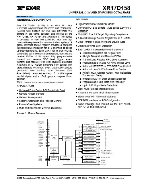
xr XR17D158UNIVERSAL (3.3V AND 5V) PCI BUS OCTAL UART NOVEMBER 2004REV. 1.2.1GENERAL DESCRIPTIONThe XR17D1581 (D158) is an octal PCI Bus Universal Asynchronous Receiver and Transmitter (UART) with support for PCI Bus universal VIO buffers in the same package and pin-out as the XR17C158, XR17C154 and XR17D154. The device is designed to meet the 32-bit PCI Bus and high bandwidth requirement in communication systems. A global interrupt source register provides a complete interrupt status indication for all 8 channels to speed up interrupt parsing. Each UART has its own 16C550 compatible set of configuration registers, transmit and receive FIFOs of 64 bytes, fully programmable transmit and receive FIFO level trigger levels, transmit and receive FIFO level counters, automatic RTS/CTS or DTR/DSR hardware flow control with programmable hysteresis levels, automatic software (Xon/Xoff) flow control, IrDA (Infrared Data Association) encoder/decoder, 8 multi-purpose inputs/outputs and a 16-bit general purpose timer/ counter.N OTE: 1 Covered by U.S. Patents #5,649,122 and #5,949,787 APPLICATIONS•Universal Form Factor PCI Bus Add-in Card •Remote Access Servers•Network Management•Factory Automation and Process Control•Point-of-Sale Systems•Multi-port RS-232/RS-422/RS-485 Cards FEATURES•High Performance Octal PCI UART•Universal PCI Bus Buffers - Auto-sense 3.3V or 5V Operation•32-bit PCI Bus 2.3 Target Signalling Compliance •A Global Interrupt Source Register for all 8 UARTs •Data Transfer in Byte, Word and Double-word •Data Read/Write Burst Operation•Each UART is independently controlled with:■16C550 Compatible 5G Register Set■64-byte Transmit and Receive FIFOs■Transmit and Receive FIFO Level Counters■Programmable TX and RX FIFO Trigger Level■Automatic RTS/CTS or DTR/DSR Flow Control■Automatic Xon/Xoff Software Flow Control■RS485 HDX Control Output with Selectable Turn-around Delay■Infrared (IrDA 1.0) Data Encoder/Decoder■Programmable Data Rate with Prescaler■Up to 6.25 Mbps Serial Data Rate•Eight Multi-Purpose Inputs/outputs•A General Purpose 16-bit Timer/counter•Sleep Mode with Automatic Wake-up •EEPROM Interface for PCI Configuration•Same Package and Pin-out as the XR17C158, XR17C154 and XR17D154F IGURE 1. B LOCK D IAGRAMExar Corporation 48720 Kato Road, Fremont CA, 94538 • (510) 668-7000 • FAX (510) 668-7017 • XR17D158xrUNIVERSAL (3.3V AND 5V) PCI BUS OCTAL UART REV. 1.2.12F IGURE 2. P IN O UT OF THE D EVICEORDERING INFORMATIONP ART N UMBER P ACKAGE O PERATING T EMPERATURE R ANGED EVICE S TATUSXR17D158CV 144-Lead TQFP 0°C to +70°C Active XR17D158IV144-Lead TQFP-40°C to +85°CActivexrXR17D158REV. 1.2.1UNIVERSAL (3.3V AND 5V) PCI BUS OCTAL UART3PIN DESCRIPTIONSN AMEP IN #T YPED ESCRIPTIONPCI LOCAL BUS INTERFACERST#134IPCI bus reset input (active low). It resets the PCI local bus configurationspace registers, device configuration registers and UART channel registers to the default condition.CLK 135I PCI bus clock input of up to 33.34MHz.AD31-AD25,AD24,AD23-AD16, AD15-AD8, AD7-AD0138-144,1,6-13,26-33,37-44IOAddress data lines [31:0] (bidirectional).FRAME#15I Bus transaction cycle frame (active low). It indicates the beginning and dura-tion of an access.C/BE0#-C/BE3#36,25,14,2IBus Command/Byte Enable [3:0] (active low). This line is multiplexed for bus Command during the address phase and Byte Enables during the data phase.IRDY#16IInitiator Ready (active low). During a write, it indicates that valid data ispresent on data bus. During a read, it indicates the master is ready to accept data.TRDY#17O Target Ready (active low).STOP#21O Target request to stop current transaction (active low). IDSEL 3I Initialization device select (active high). DEVSEL#18O Device select to the XR17D158 (active low).INTA#133OD Device interrupt from XR17D158 (open drain, active low).PAR 24IO Parity is even across AD[31:0] and C/BE[3:0]# (bidirectional, active high). PERR#22O Data Parity error indicator, except for Special Cycle transactions (active low). Optional in bus target application.SERR#23ODSystem error indicator, Address parity or Data parity during Special Cycle transactions (open drain, active low). Optional in bus target application.MODEM OR SERIAL I/O INTERFACETX0125O UART channel 0 Transmit Data or infrared transmit data. Normal TXD output idles HIGH while infrared TXD output idles LOW.RX0132IUART channel 0 Receive Data or infrared receive data. Normal RXD input idles HIGH. The infrared pulses typically idle LOW but can be inverted inter-nally prior the decoder by FCTR[4].RTS0#127O UART channel 0 Request to Send or general purpose output (active low).CTS0#131I UART channel 0 Clear to Send or general purpose input (active low).DTR0#126O UART channel 0 Data Terminal Ready or general purpose output (active low).DSR0#130I UART channel 0 Data Set Ready or general purpose input (active low).CD0#129IUART channel 0 Carrier Detect or general purpose input (active low).XR17D158xrUNIVERSAL (3.3V AND 5V) PCI BUS OCTAL UARTREV. 1.2.14RI0#128I UART channel 0 Ring Indicator or general purpose input (active low).TX1117O UART channel 1 Transmit Data or infrared transmit data. Normal TXD output idles HIGH while infrared TXD output idles LOW.RX1124IUART channel 1 Receive Data or infrared receive data. Normal RXD input idles HIGH. The infrared pulses typically idle LOW but can be inverted inter-nally prior the decoder by FCTR[4].RTS1#119O UART channel 1 Request to Send or general purpose output (active low).CTS1#123I UART channel 1 Clear to Send or general purpose input (active low).DTR1#118O UART channel 1 Data Terminal Ready or general purpose output (active low).DSR1#122I UART channel 1 Data Set Ready or general purpose input (active low).CD1#121I UART channel 1 Carrier Detect or general purpose input (active low).RI1#120I UART channel 1 Ring Indicator or general purpose input (active low).TX2106O UART channel 2 Transmit Data or infrared transmit data. Normal TXD output idles HIGH while infrared TXD output idles LOW.RX299IUART channel 2 Receive Data or infrared receive data. Normal RXD input idles HIGH. The infrared pulses typically idle LOW but can be inverted inter-nally prior the decoder by FCTR[4].RTS2#104O UART channel 2 Request to Send or general purpose output (active low).CTS2#100I UART channel 2 Clear to Send or general purpose input (active low).DTR2#105O UART channel 2 Data Terminal Ready or general purpose output (active low).DSR2#101I UART channel 2 Data Set Ready or general purpose input (active low).CD2#102I UART channel 2 Carrier Detect or general purpose input (active low).RI2#103I UART channel 2 Ring Indicator or general purpose input (active low).TX398O UART channel 3 Transmit Data or infrared transmit data. Normal TXD output idles HIGH while infrared TXD output idles LOW.RX391IUART channel 3 Receive Data or infrared receive data. Normal RXD input idles HIGH. The infrared pulses typically idle LOW but can be inverted inter-nally prior the decoder by FCTR[4].RTS3#96O UART channel 3 Request to Send or general purpose output (active low).CTS3#92I UART channel 3 Clear to Send or general purpose input (active low).d.DTR3#97O UART channel 3 Data Terminal Ready or general purpose output (active low).DSR3#93I UART channel 3 Data Set Ready or general purpose input (active low).CD3#94I UART channel 3 Carrier Detect or general purpose input (active low).RI3#95I UART channel 3 Ring Indicator or general purpose input (active low).TX488O UART channel 4 Transmit Data or infrared transmit data. Normal TXD output idles HIGH while infrared TXD output idles LOW.RX481IUART channel 4 Receive Data or infrared receive data. Normal RXD input idles HIGH. The infrared pulses typically idle LOW but can be inverted inter-nally prior the decoder by FCTR[4].PIN DESCRIPTIONSN AME P IN#T YPE D ESCRIPTIONxrXR17D158REV. 1.2.1UNIVERSAL (3.3V AND 5V) PCI BUS OCTAL UART5RTS4#86O UART channel 4 Request to Send or general purpose output (active low).CTS4#82I UART channel 4 Clear to Send or general purpose input (active low).DTR4#87O UART channel 4 Data Terminal Ready or general purpose output (active low).DSR4#83I UART channel 4 Data Set Ready or general purpose input (active low).CD4#84I UART channel 4 Carrier Detect or general purpose input (active low).RI4#85I UART channel 4 Ring Indicator or general purpose input (active low).TX580O UART channel 5 Transmit Data or infrared transmit data. Normal TXD output idles HIGH while infrared TXD output idles LOW.RX571IUART channel 5 Receive Data or infrared receive data. Normal RXD input idles HIGH. The infrared pulses typically idle LOW but can be inverted inter-nally prior the decoder by FCTR[4].RTS5#78O UART channel 5 Request to Send or general purpose output (active low).CTS5#72I UART channel 5 Clear to Send or general purpose input (active low).DTR5#79O UART channel 5 Data Terminal Ready or general purpose output (active low).DSR5#75I UART channel 5 Data Set Ready or general purpose input (active low).CD5#76I UART channel 5 Carrier Detect or general purpose input (active low).RI5#77I UART channel 5 Ring Indicator or general purpose input (active low).TX662O UART channel 6 Transmit Data or infrared transmit data. Normal TXD output idles HIGH while infrared TXD output idles LOW.RX655IUART channel 6 Receive Data or infrared receive data. Normal RXD input idles HIGH. The infrared pulses typically idle LOW but can be inverted inter-nally prior the decoder by FCTR[4].RTS6#60O UART channel 6 Request to Send or general purpose output (active low).CTS6#56I UART channel 6 Clear to Send or general purpose input (active low).DTR6#61O UART channel 6 Data Terminal Ready or general purpose output (active low).DSR6#57I UART channel 6 Data Set Ready or general purpose input (active low).CD6#58I UART channel 6 Carrier Detect or general purpose input (active low).RI6#59I UART channel 6 Ring Indicator or general purpose input (active low).TX754O UART channel 7 Transmit Data or infrared transmit data. Normal TXD output idles HIGH while infrared TXD output idles LOW.RX747IUART channel 7 Receive Data or infrared receive data. Normal RXD input idles HIGH. The infrared pulses typically idle LOW but can be inverted inter-nally prior the decoder by FCTR[4].RTS7#52O UART channel 7 Request to Send or general purpose output (active low).CTS7#48I UART channel 7 Clear to Send or general purpose input (active low).DTR7#53O UART channel 7 Data Terminal Ready or general purpose output (active low).DSR7#49IUART channel 7 Data Set Ready or general purpose input (active low).PIN DESCRIPTIONSN AME P IN#T YPE D ESCRIPTIONXR17D158xrUNIVERSAL (3.3V AND 5V) PCI BUS OCTAL UARTREV. 1.2.16CD7#50I UART channel 7 Carrier Detect or general purpose input (active low).RI7#51IUART channel 7 Ring Indicator or general purpose input (active low).ANCILLARY SIGNALSMPIO0108I/O Multi-purpose input/output 0. The function of this pin is defined thru the Con-figuration Register MPIOSEL, MPIOLVL, MPIOINV, MPIO3T and MPIOINT MPIO1107I/O Multi-purpose input/output 1. The function of this pin is defined thru the Con-figuration Register MPIOSEL, MPIOLVL, MPIOINV, MPIO3T and MPIOINT.MPIO274I/O Multi-purpose input/output 2. The function of this pin is defined thru the Con-figuration Register MPIOSEL, MPIOLVL, MPIOINV, MPIO3T and MPIOINT.MPIO373I/O Multi-purpose input/output 3. The function of this pin is defined thru the Con-figuration Register MPIOSEL, MPIOLVL, MPIOINV, MPIO3T and MPIOINT.MPIO468I/O Multi-purpose input/output 4. The function of this pin is defined thru the Con-figuration Register MPIOSEL, MPIOLVL, MPIOINV, MPIO3T and MPIOINT.MPIO567I/O Multi-purpose input/output 5. The function of this pin is defined thru the Con-figuration Register MPIOSEL, MPIOLVL, MPIOINV, MPIO3T and MPIOINT.MPIO666I/O Multi-purpose input/output 6. The function of this pin is defined thru the Con-figuration Register MPIOSEL, MPIOLVL, MPIOINV, MPIO3T and MPIOINT.MPIO765I/O Multi-purpose input/output 7. The function of this pin is defined thru the Con-figuration Register MPIOSEL, MPIOLVL, MPIOINV, MPIO3T and MPIOINT.EECK116OSerial clock to EEPROM. An internal clock of CLK divide by 256 is used for reading the vendor and sub-vendor ID during power up or reset. However, it can be manually clocked thru the Configuration Register REGB.EECS 115OChip select to a EEPROM device like 93C46. It is manually selectable thru the Configuration Register REGB. Requires a pull-up 4.7K ohm resistor for external sensing of EEPROM during power up. See DAN112 for further details.EEDI 114O Write data to EEPROM device. It is manually accessible thru the Configura-tion Register REGB.EEDO 113I Read data from EEPROM device. It is manually accessible thru the Configu-ration Register REGB.XTAL1110I Crystal or external clock input.XTAL2109O Crystal or buffered clock output. TMRCK 69I 16-bit timer/counter external clock input.ENIR70IInfrared mode enable (active high). This pin is sampled during power up, fol-lowing a hardware reset (RST#) or soft-reset (register RESET). It can be used to start up all 8 UARTs in the infrared mode. The sampled logic state is transferred to MCR bit-6 in the UART.TEST#111IFactory Test. Connect to VCC for normal operation.VCC64, 90,112Power supply for the UART core logic - 5V ONLY . This power supply deter-mines the VOH level of the non-PCI bus interface outputs. See Table 1 for valid combinations of VCC and VIO that can be used for the XR17D158.PIN DESCRIPTIONSN AME P IN #T YPE D ESCRIPTIONxrXR17D158REV. 1.2.1UNIVERSAL (3.3V AND 5V) PCI BUS OCTAL UART7N OTE : Pin type: I=Input, O=Output, IO= Input/output, OD=Output Open Drain.VIO4, 19, 34, 45,137PCI Bus I/O Power supply - 3.3V or 5V, detected by the auto-sense circuitry of the XR17D158. This power supply determines the VOH level of the PCI bus interface outputs.(PCI 2.3 signalling compliant at both 3.3V and 5V operation, suitable for uni-versal form factor add-in card application)GND5,20,35,46,63,89,136Power supply common, ground.PIN DESCRIPTIONSN AME P IN#T YPED ESCRIPTIONXR17D158xrUNIVERSAL (3.3V AND 5V) PCI BUS OCTAL UARTREV. 1.2.18FUNCTIONAL DESCRIPTIONThe XR17D158 (D158) integrates the functions of 8 enhanced 16550 UARTs with the PCI Local Bus interface and a non-volatile memory interface for PCI bus’s plug-and-play auto-configuration, a 16-bit timer/counter, 8 multi-purpose inputs/outputs, and an on-chip oscillator. The PCI local bus is a synchronous timing bus where all bus transactions are associated to the bus clock of up to 33MHz. The D158 supports 32-bit wide read and write data transfer operations including data burst mode through the PCI Local Bus interface. Read and write data operations may be in byte, word or double-word (DWORD) format. A single 32-bit interrupt status register provides interrupts status for all 8 UARTs, timer/counter, multipurpose inputs/outputs, and a special sleep wake up indicator. There are three sets of register in the device. First, the PCI local bus configuration registers for PCI auto configuration. A set of device configuration registers for overall control, 32-bit wide transmit and receive data transfer, and monitoring of the 8 UART channels. Lastly, each UART channel has its own 16550 UART compatible configuration register set for individual channel control, status, and byte wide data transfer.Each UART has 64-byte FIFOs, automatic RTS/CTS or DTR/DSR hardware flow control with hysteresis control, automatic Xon/Xoff and special character software flow control, programmable transmit and receive FIFO trigger level, FIFO level counters, infrared encoder and decoder (IrDA ver. 1.0), programmable baud rate generator with a prescaler of 1X or 4X, and data rate up to 6.25 Mbps at 8X sampling clock.The XR17D158 is available in a thin 144-pin TQFP (20x20x1.4mm) package in commercial and industrial temperature ranges.PCI L OCAL B US I NTERFACEThis is the host interface and it meets the PCI Local Bus Specification revision 2.3. The PCI local bus operations are synchronous meaning each transaction is associated to the bus clock. The XR17D158 can operate with the bus clock of up to a 33.34MHz. Data transfers operation can be formatted in 8-bit, 16-bit, 24-bit or 32-bit wide. With 32-bit data operations, it pushes the data transfer rate on the bus up to 132 MByte/sec. This increases the overall system’s communication performance up to 16 times better than the 8-bit ISA bus. See PCI local bus specification revision 2.3 for bus operation details.PCI L OCAL B US C ONFIGURATION S PACE R EGISTERSA set of PCI local bus configuration space register is provided. These registers provide the PCI local bus operating system with the card’s vendor ID, device ID, sub-vendor ID, product model number, and resources and capabilities. The PCI local bus operating system collects this data from all the cards on the bus during the auto configuration phase that follows immediately after a power up or system reset/reboot. After it has sorted out all devices on the bus, it defines and download the operating conditions to the cards. One of the definitions is the base address loaded into the Base Address Register (BAR) where the card will be operating in the PCI local bus memory space.EEPROM I NTERFACEAn external 93C46 EEPROM is only used to store the vendor’s ID and model number, and the sub-vendor’s ID and product model number. This information is only used with the plug-and-play auto configuration of the PCI local bus. These data provide automatic hardware installation onto the PCI bus. The EEPROM interface consists of 4 signals, EEDI, EEDO, EECS, and EECK. The EEPROM is not needed when auto configuration is not required in the application. However, If your design requires non-volatile memory for other purpose. It is possible to store and retrieve data on the EEPROM through a special PCI device configuration register. See application note DAN112 for its programming details.xr XR17D158 REV. 1.2.1UNIVERSAL (3.3V AND 5V) PCI BUS OCTAL UART 1.0APPLICATION EXAMPLESThe XR17D158 is designed to operate with VCC (voltage to the UART Core Logic) at 5V only, irrespective of whether the PCI bus is at 3.3V or 5V. Table 1 below shows the valid combinations of VCC and the PCI Bus Voltage, VIO that can be used for the device..T ABLE 1: V ALID C OMBINATIONS OF VCC AND VIO S UPPLY V OLTAGESVCC VIO5.0V 5.0V Valid5.0V 3.3V Valid3.3V 5.0V Invalid3.3V 3.3V InvalidA typical application for a universal add-in card (VCC must be 5V) is shown in Figure 3. In an embedded system, the designer must still choose 5V power supply for the VCC regardless of VIO (3.3 or 5V). In Figure 4, examples 1 and 2 show valid applications of the XR17D158 in an embedded system.F IGURE 3. T YPICAL A PPLICATION FOR A U NIVERSAL A DD-IN C ARD9XR17D158xrUNIVERSAL (3.3V AND 5V) PCI BUS OCTAL UART REV. 1.2.110F IGURE 4. T YPICAL A PPLICATIONS IN AN E MBEDDED S YSTEM2.0XR17D158 REGISTERSThe XR17D158 UART has three different sets of registers as shown in Figure 5. The PCI local bus configuration space registers are for plug-and-play auto-configuration when connecting the device to a the PCI bus. This auto-configuration feature makes installation very easy into a PCI system and it is part of the PCI local bus specification. The second register set is the device configuration registers that are accessible directly from the PCI bus for programming general operating conditions of the device and monitoring the status of various functions. These registers are mapped into 4K of the PCI bus memory address space. These functions include all 8 channel UART’s interrupt control and status, 16-bit general purpose timer control and status, multipurpose inputs/outputs control and status, sleep mode, soft-reset, and device identification and revision. And lastly, each UART channel has its own set of internal UART configuration registers for its own operation control and status reporting. All 8 sets of channel registers are embedded inside the device configuration registers space, which provides faster access. The following paragraphs describe all 3 sets of registers in detail.F IGURE 5. T HE XR17D158 R EGISTER S ETS2.1PCI LOCAL BUS CONFIGURATION SPACE REGISTERSThe PCI local bus configuration space registers are responsible for setting up the device’s operating environment in the PCI local bus. The pre-defined operating parameters of the device is read by the PCI bus plug-and-play auto-configuration manager in the operating system. After the PCI bus has collected all data from every device/card on the bus, it defines and downloads the memory mapping information to each device/ card about their individual operation memory address location and conditions. The operating memory mapped address location is downloaded into the Base Address Register (BAR) register, 0x10. The plug-and-play auto configuration feature is only available when an external 93C46 EEPROM is used. The EEPROM contains the device vendor and sub-vendor data required by the auto-configuration setup.UNIVERSAL (3.3V AND 5V) PCI BUS OCTAL UART REV. 1.2.1 T ABLE 2: PCI L OCAL B US C ONFIGURATION S PACE R EGISTERSA DDRESSB ITS T YPE D ESCRIPTION R ESET V ALUE(HEX)0x0031:16RWR1Device ID (Exar device ID number)0x0158 15:0RWR1Vendor ID (Exar) specified by PCISIG0x13A80x04313029:28RWCRWCROParity error detected. Cleared by writing a logic 1.System error detected. Cleared by writing a logic 1.Unused000027R-Reset Target Abort. Set whenever D158 terminates with a target abort. 026:25RO DEVSEL# timing. 0024RO Unemployments bus master error reporting bit023RO Fast back to back transactions are supported122:16RO Reserved Status bits000 000015:9,7,5,4,3,2RO Command bits (reserved)0x00008RWR SERR# driver enable. Logic 1=enable driver and 0=disabledriver0 6RWR Parity error enable. Logic 1=respond to parity error and 0=ignore01RWR Command controls a device’s response to mem space accesses:0=disable mem space accesses, 1=enable mem space accesses0RO Device’s response to I/O space accesses is disabled.(0 = disable I/O space accesses)0x0831:8RO Class Code (Simple 550 Communication Controller). 0x070002 7:0RO Revision ID (Exar device revision number) Current Rev. value 0x0C31:24RO BIST (Built-in Self Test)0x00 23:16RO Header Type (a single function device with one BAR) 0x0015:8RO Unimplemented Latency Timer (needed only for bus master)0x007:0RO Unimplemented Cache Line Size 0x000x1031:12RWR Memory Base Address Register (BAR)0x00 11:0RO Claims a 4K address space for the memory mapped UARTs0x0000x1431:0RO Unimplemented Base Address Register (returns zeros)0x000000000x18h31:0RO Unimplemented Base Address Register (returns zeros)0x000000000x1C31:0RO Unimplemented Base Address Register (returns zeros)0x000000000x2031:0RO Unimplemented Base Address Register (returns zeros)0x000000000x2431:0RO Unimplemented Base Address Register (returns zeros)0x000000000x2831:0RO Reserved 0x00000000N OTE : RWR 1=Read/Write from external EEPROM. RWR=Read/Write from AD[31:0]. RO= Read Only. RWC=Read/Write-Clear.2.2Device Configuration Register SetThe device configuration registers and a special way to access each of the UART’s transmit and receive data FIFOs are accessible directly from the PCI data bus. This provides easy programming of general operating parameters to the D158 UART and for monitoring the status of various functions. The registers occupy 4K of PCI bus memory address space. These addresses are offset onto the basic memory address, a value loaded into the Memory Base Address Register (BAR) in the PCI local bus configuration register set. These registers control or report on all 8 channel UARTs functions that include interrupt control and status, 16-bit general purpose timer control and status, multipurpose inputs/outputs control and status, sleep mode control, soft-reset control, and device identification and revision, and others.The registers set is mapped into 8 address blocks where each UART channel occupies 512 bytes memory space for its own 16550 compatible configuration registers. The device configuration and control registers are embedded inside the UART channel zero’s address space between 0x0080 to 0x0093. All these registers can be accessed in 8, 16, 24 or 32 bit width depending on the starting address given by the host at beginning of the bus cycle. Transmit and receive data may be loaded or unloaded in 8, 16, 24 or 32 bit format to the register’s address. Every time a read or write operation is made to the transmit or receive register, its FIFO data pointer is automatically bumped to the next sequential data location either in byte, word or dword. One special case applies to the receive data unloading when reading the receive data together with its LSR register content. The host must read them in 16 or 32 bits format in order to maintain integrity of the data byte with its associated error flags.0x2C31:16RWR 1Subsystem ID (write from external EEPROM by customer)0x000015:0RWR 1Subsystem Vendor ID (write from external EEPROM by cus-tomer)0x00000x3031:0RO Expansion ROM Base Address (Unimplemented)0x000000000x3431:0RO Reserved (returns zeros)0x000000000x3831:0RO Reserved (returns zeros)0x000000000x3C31:24RO Unimplemented MAXLAT 0x0023:16RO Unimplemented MINGNT 0x0015:8RO Interrupt Pin, use INTA#. 0x017:0RWRInterrupt Line.0xXXT ABLE 2: PCI L OCAL B US C ONFIGURATION S PACE R EGISTERSA DDRESSB ITS T YPE D ESCRIPTIONR ESET V ALUE(HEX )UNIVERSAL (3.3V AND 5V) PCI BUS OCTAL UART REV. 1.2.1T ABLE 3: XR17D158 D EVICE C ONFIGURATION R EGISTERSO FFSET A DDRESS M EMORY S PACE R EAD/W RITE D ATA W IDTH C OMMENT0x000 - 0x00F UART channel 0 Regs (Table 12 & Table 13)8/16/24/32First 8 regs are 16550 compatible0x010 - 0x07F Reserved0x080 - 0x093DEVICE CONFIG.(Table 4)8/16/24/32REGISTERS0x094 - 0x0FF Reserved0x100 - 0x13F UART 0 – Read FIFO Read-Only8/16/24/3264 bytes of RX FIFO data0x100 - 0x13F UART 0 – Write FIFO Write-Only8/16/24/3264 bytes of TX FIFO data0x140 - 0x17F ReservedRead-Only16/3264 bytes of RX FIFO data + LSR0x180 - 0x1FF UART 0 – Read FIFOwith errors0x200 - 0x20F UART channel 1 Regs (Table 12 & Table 13)8/16//24/32First 8 regs are 16550 compatible0x210 - 0x2FF Reserved0x300 - 0x33F UART 1 – Read FIFO Read-Only8/16/24/3264 bytes of RX FIFO data0x300 - 0x33F UART 1 – Write FIFO Write-Only8/16/24/3264 bytes of TX FIFO data0x340 - 0x37F Reserved0x380 - 0x3FF UART 1 – Read FIFORead-Only16/3264 bytes of RX FIFO data + LSR with errors0x400 - 0x40F UART channel 2 Regs (Table 12 & Table 13)8/16/24/32First 8 regs are 16550 compatible0x410 - 0x4FF Reserved0x500 - 0x53F UART 2 – Read FIFO Read-Only8/16/24/3264 bytes of RX FIFO data0x500 - 0x53F UART 2 – Write FIFO Write-Only8/16/24/3264 bytes of TX FIFO data0x540 - 0x57F ReservedRead-Only16/3264 bytes of RX FIFO data + LSR0x580 - 0x5FF UART 2 – Read FIFOwith errors0x600 - 0x60F UART channel 3 Regs (Table 12 & Table 13)8/16/24/32First 8 regs are 16550 compatible0x610 - 0x6FF Reserved0x700 - 0x73F UART 3 – Read FIFO Read-Only8/16/24/3264 bytes of RX FIFO data0x700 - 0x73F UART 3 – Write FIFO Write-Only8/16/24/3264 bytes of TX FIFO data0x740 - 0x77F ReservedRead-Only16/3264 bytes of RX FIFO data + LSR0x780 - 0x7FF UART 3 – Read FIFOwith errors。