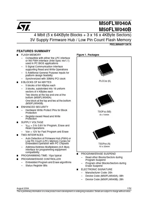
M50FLW040BNB1P中文资料
- 格式:pdf
- 大小:435.87 KB
- 文档页数:52
1/52PRELIMINARY DATAAugust 2004This is preliminary information on a new product now in development or undergoing evaluation. Details are subject to change without notice.M50FLW040A M50FLW040B4 Mbit (5 x 64KByte Blocks + 3 x 16 x 4KByte Sectors)3V Supply Firmware Hub / Low Pin Count Flash MemoryFEATURES SUMMARYsFLASH MEMORY–Compatible with either the LPC interfaceor the FWH interface (Intel Spec rev1.1) used in PC BIOS applications– 5 Signal Communication Interfacesupporting Read and Write Operations – 5 Additional General Purpose Inputs forplatform design flexibility–Synchronized with 33MHz PCI clock s8 BLOCKS OF 64 KBYTES – 5 blocks of 64 KBytes each– 3 blocks, subdivided into 16 uniformsectors of 4 KBytes eachTwo blocks at the top and one at the bottom (M50FLW040A)One block at the top and two at the bottom (M50FLW040B)sENHANCED SECURITY–Hardware Write Protect Pins for BlockProtection–Register-based Read and WriteProtectionsSUPPLY VOLTAGE–V CC = 3 to 3.6V for Program, Erase andRead Operations–V PP = 12V for Fast Program and Erase sTWO INTERFACES–Auto Detection of Firmware Hub (FWH) orLow Pin Count (LPC) Memory Cycles for Embedded Operation with PC Chipsets –Address/Address Multiplexed (A/A Mux)Interface for programming equipment compatibility.s PROGRAMMING TIME: 10µs typical sPROGRAM/ERASE CONTROLLER–Embedded Program and Erase algorithms –Status Register BitssPROGRAM/ERASE SUSPEND–Read other Blocks/Sectors duringProgram Suspend–Program other Blocks/Sectors duringErase SuspendsELECTRONIC SIGNATURE –Manufacturer Code: 20h–Device Code (M50FLW040A): 08h –Device Code (M50FLW040B): 28hM50FLW040A, M50FLW040BTABLE OF CONTENTSFEATURES SUMMARY . . . . . . . . . . . . . . . . . . . . . . . . . . . . . . . . . . . . . . . . . . . . . . . . . . . . . . . . . . . . .1 Figure 1.Packages. . . . . . . . . . . . . . . . . . . . . . . . . . . . . . . . . . . . . . . . . . . . . . . . . . . . . . . . . . . . . .1SUMMARY DESCRIPTION. . . . . . . . . . . . . . . . . . . . . . . . . . . . . . . . . . . . . . . . . . . . . . . . . . . . . . . . . . .6Figure 2.Logic Diagram (FWH/LPC Interface). . . . . . . . . . . . . . . . . . . . . . . . . . . . . . . . . . . . . . . . .7 Figure 3. Logic Diagram (A/A Mux Interface). . . . . . . . . . . . . . . . . . . . . . . . . . . . . . . . . . . . . . . . . .7 Table 1.Signal Names (FWH/LPC Interface) . . . . . . . . . . . . . . . . . . . . . . . . . . . . . . . . . . . . . . . . .7 Table 2.Signal Names (A/A Mux Interface) . . . . . . . . . . . . . . . . . . . . . . . . . . . . . . . . . . . . . . . . . .7 Figure 4.PLCC Connections . . . . . . . . . . . . . . . . . . . . . . . . . . . . . . . . . . . . . . . . . . . . . . . . . . . . . .8 Figure 5.TSOP32 Connections . . . . . . . . . . . . . . . . . . . . . . . . . . . . . . . . . . . . . . . . . . . . . . . . . . . .8 Figure 6.TSOP40 Connections . . . . . . . . . . . . . . . . . . . . . . . . . . . . . . . . . . . . . . . . . . . . . . . . . . . .9 Table 3.Addresses (M50FLW040A). . . . . . . . . . . . . . . . . . . . . . . . . . . . . . . . . . . . . . . . . . . . . . . .9 Table 4.Addresses (M50FLW040B). . . . . . . . . . . . . . . . . . . . . . . . . . . . . . . . . . . . . . . . . . . . . . . .9SIGNAL DESCRIPTIONS. . . . . . . . . . . . . . . . . . . . . . . . . . . . . . . . . . . . . . . . . . . . . . . . . . . . . . . . . . .10Firmware Hub/Low Pin Count (FWH/LPC) Signal Descriptions . . . . . . . . . . . . . . . . . . . . . . . .10 Input/Output Communications (FWH0/LAD0-FWH3/LAD3).. . . . . . . . . . . . . . . . . . . . . . . . . . . . . .10 Input Communication Frame (FWH4/LFRAME).. . . . . . . . . . . . . . . . . . . . . . . . . . . . . . . . . . . . . . .10 Identification Inputs (ID0-ID3).. . . . . . . . . . . . . . . . . . . . . . . . . . . . . . . . . . . . . . . . . . . . . . . . . . . . .10 General Purpose Inputs (GPI0-GPI4).. . . . . . . . . . . . . . . . . . . . . . . . . . . . . . . . . . . . . . . . . . . . . . .10 Interface Configuration (IC). . . . . . . . . . . . . . . . . . . . . . . . . . . . . . . . . . . . . . . . . . . . . . . . . . . . . . .1010 CPU Reset (INIT).. . . . . . . . . . . . . . . . . . . . . . . . . . . . . . . . . . . . . . . . . . . . . . . . . . . . . . . . . . . . . .10 Clock (CLK). . . . . . . . . . . . . . . . . . . . . . . . . . . . . . . . . . . . . . . . . . . . . . . . . . . . . . . . . . . . . . . . . . .10 Top Block Lock (TBL).. . . . . . . . . . . . . . . . . . . . . . . . . . . . . . . . . . . . . . . . . . . . . . . . . . . . . . . . . . .1011 Reserved for Future Use (RFU).. . . . . . . . . . . . . . . . . . . . . . . . . . . . . . . . . . . . . . . . . . . . . . . . . . .11 Address/Address Multiplexed (A/A Mux) Signal Descriptions . . . . . . . . . . . . . . . . . . . . . . . . .11 Address Inputs (A0-A10). . . . . . . . . . . . . . . . . . . . . . . . . . . . . . . . . . . . . . . . . . . . . . . . . . . . . . . . .11 Data Inputs/Outputs (DQ0-DQ7). . . . . . . . . . . . . . . . . . . . . . . . . . . . . . . . . . . . . . . . . . . . . . . . . . .11 Output Enable (G). . . . . . . . . . . . . . . . . . . . . . . . . . . . . . . . . . . . . . . . . . . . . . . . . . . . . . . . . . . . . .11 . . . . . . . . . . . . . . . . . . . . . . . . . . . . . . . . . . . . . . . . . . . . . . . . . . . . . . . . . . . . . .11 Row/Column Address Select (RC).. . . . . . . . . . . . . . . . . . . . . . . . . . . . . . . . . . . . . . . . . . . . . . . . .11 Ready/Busy Output (RB). . . . . . . . . . . . . . . . . . . . . . . . . . . . . . . . . . . . . . . . . . . . . . . . . . . . . . . . .11 Supply Signal Descriptions . . . . . . . . . . . . . . . . . . . . . . . . . . . . . . . . . . . . . . . . . . . . . . . . . . . . .11 V CC Supply Voltage. . . . . . . . . . . . . . . . . . . . . . . . . . . . . . . . . . . . . . . . . . . . . . . . . . . . . . . . . . . . .11 V PP Optional Supply Voltage. . . . . . . . . . . . . . . . . . . . . . . . . . . . . . . . . . . . . . . . . . . . . . . . . . . . . .11 V SS Ground. . . . . . . . . . . . . . . . . . . . . . . . . . . . . . . . . . . . . . . . . . . . . . . . . . . . . . . . . . . . . . . . . . .11 Table 5.Memory Identification Input Configuration (LPC mode). . . . . . . . . . . . . . . . . . . . . . . . . .12BUS OPERATIONS. . . . . . . . . . . . . . . . . . . . . . . . . . . . . . . . . . . . . . . . . . . . . . . . . . . . . . . . . . . . . . . .12Firmware Hub/Low Pin Count (FWH/LPC) Bus Operations. . . . . . . . . . . . . . . . . . . . . . . . . . . .12 Bus Read. . . . . . . . . . . . . . . . . . . . . . . . . . . . . . . . . . . . . . . . . . . . . . . . . . . . . . . . . . . . . . . . . . . . .122/52M50FLW040A, M50FLW040BBus Write. . . . . . . . . . . . . . . . . . . . . . . . . . . . . . . . . . . . . . . . . . . . . . . . . . . . . . . . . . . . . . . . . . . . .12 Bus Abort. . . . . . . . . . . . . . . . . . . . . . . . . . . . . . . . . . . . . . . . . . . . . . . . . . . . . . . . . . . . . . . . . . . . .13 Standby. . . . . . . . . . . . . . . . . . . . . . . . . . . . . . . . . . . . . . . . . . . . . . . . . . . . . . . . . . . . . . . . . . . . . .13 Reset. . . . . . . . . . . . . . . . . . . . . . . . . . . . . . . . . . . . . . . . . . . . . . . . . . . . . . . . . . . . . . . . . . . . . . . .13 Block Protection. . . . . . . . . . . . . . . . . . . . . . . . . . . . . . . . . . . . . . . . . . . . . . . . . . . . . . . . . . . . . . . .13 Address/Address Multiplexed (A/A Mux) Bus Operations. . . . . . . . . . . . . . . . . . . . . . . . . . . . .13 Bus Read. . . . . . . . . . . . . . . . . . . . . . . . . . . . . . . . . . . . . . . . . . . . . . . . . . . . . . . . . . . . . . . . . . . . .13 Bus Write. . . . . . . . . . . . . . . . . . . . . . . . . . . . . . . . . . . . . . . . . . . . . . . . . . . . . . . . . . . . . . . . . . . . .13 Output Disable. . . . . . . . . . . . . . . . . . . . . . . . . . . . . . . . . . . . . . . . . . . . . . . . . . . . . . . . . . . . . . . . .13 Reset. . . . . . . . . . . . . . . . . . . . . . . . . . . . . . . . . . . . . . . . . . . . . . . . . . . . . . . . . . . . . . . . . . . . . . . .13 Table 6.FWH Bus Read Field Definitions. . . . . . . . . . . . . . . . . . . . . . . . . . . . . . . . . . . . . . . . . . .14 Figure 7.FWH Bus Read Waveforms. . . . . . . . . . . . . . . . . . . . . . . . . . . . . . . . . . . . . . . . . . . . . . .14 Table 7.FWH Bus Write Field Definitions. . . . . . . . . . . . . . . . . . . . . . . . . . . . . . . . . . . . . . . . . . .15 Figure 8.FWH Bus Write Waveforms. . . . . . . . . . . . . . . . . . . . . . . . . . . . . . . . . . . . . . . . . . . . . . .15 Table 8.LPC Bus Read Field Definitions (1-Byte). . . . . . . . . . . . . . . . . . . . . . . . . . . . . . . . . . . . .16 Figure 9.LPC Bus Read Waveforms (1-Byte) . . . . . . . . . . . . . . . . . . . . . . . . . . . . . . . . . . . . . . . .16 Table 9.LPC Bus Write Field Definitions (1 Byte). . . . . . . . . . . . . . . . . . . . . . . . . . . . . . . . . . . . .17 Figure 10.LPC Bus Write Waveforms (1 Byte) . . . . . . . . . . . . . . . . . . . . . . . . . . . . . . . . . . . . . . . .17 Table 10.A/A Mux Bus Operations. . . . . . . . . . . . . . . . . . . . . . . . . . . . . . . . . . . . . . . . . . . . . . . . .17COMMAND INTERFACE . . . . . . . . . . . . . . . . . . . . . . . . . . . . . . . . . . . . . . . . . . . . . . . . . . . . . . . . . . .18Table mand Codes. . . . . . . . . . . . . . . . . . . . . . . . . . . . . . . . . . . . . . . . . . . . . . . . . . . . . . .18 Read Memory Array Command. . . . . . . . . . . . . . . . . . . . . . . . . . . . . . . . . . . . . . . . . . . . . . . . . . . .18 Read Status Register Command. . . . . . . . . . . . . . . . . . . . . . . . . . . . . . . . . . . . . . . . . . . . . . . . . . .18 Read Electronic Signature Command. . . . . . . . . . . . . . . . . . . . . . . . . . . . . . . . . . . . . . . . . . . . . . .18 Table 12.Electronic Signature Codes. . . . . . . . . . . . . . . . . . . . . . . . . . . . . . . . . . . . . . . . . . . . . . .18 Program Command. . . . . . . . . . . . . . . . . . . . . . . . . . . . . . . . . . . . . . . . . . . . . . . . . . . . . . . . . . . . .18 Quadruple Byte Program Command (A/A Mux Interface). . . . . . . . . . . . . . . . . . . . . . . . . . . . . . . .19 Double/Quadruple Byte Program Command (FWH Mode). . . . . . . . . . . . . . . . . . . . . . . . . . . . . . .19 Chip Erase Command. . . . . . . . . . . . . . . . . . . . . . . . . . . . . . . . . . . . . . . . . . . . . . . . . . . . . . . . . . .19 Block Erase Command . . . . . . . . . . . . . . . . . . . . . . . . . . . . . . . . . . . . . . . . . . . . . . . . . . . . . . . . . .19 Sector Erase Command . . . . . . . . . . . . . . . . . . . . . . . . . . . . . . . . . . . . . . . . . . . . . . . . . . . . . . . . .20 Clear Status Register Command. . . . . . . . . . . . . . . . . . . . . . . . . . . . . . . . . . . . . . . . . . . . . . . . . . .20 Program/Erase Suspend Command . . . . . . . . . . . . . . . . . . . . . . . . . . . . . . . . . . . . . . . . . . . . . . . .20 Program/Erase Resume Command . . . . . . . . . . . . . . . . . . . . . . . . . . . . . . . . . . . . . . . . . . . . . . . .20 Table mands . . . . . . . . . . . . . . . . . . . . . . . . . . . . . . . . . . . . . . . . . . . . . . . . . . . . . . . . . . .21STATUS REGISTER. . . . . . . . . . . . . . . . . . . . . . . . . . . . . . . . . . . . . . . . . . . . . . . . . . . . . . . . . . . . . . .22Program/Erase Controller Status (Bit SR7). . . . . . . . . . . . . . . . . . . . . . . . . . . . . . . . . . . . . . . . . . .22 Erase Suspend Status (Bit SR6). . . . . . . . . . . . . . . . . . . . . . . . . . . . . . . . . . . . . . . . . . . . . . . . . . .22 Erase Status (Bit SR5) . . . . . . . . . . . . . . . . . . . . . . . . . . . . . . . . . . . . . . . . . . . . . . . . . . . . . . . . . .22 Program Status (Bit SR4) . . . . . . . . . . . . . . . . . . . . . . . . . . . . . . . . . . . . . . . . . . . . . . . . . . . . . . . .22 V PP Status (Bit SR3) . . . . . . . . . . . . . . . . . . . . . . . . . . . . . . . . . . . . . . . . . . . . . . . . . . . . . . . . . . . .22 Program Suspend Status (Bit SR2). . . . . . . . . . . . . . . . . . . . . . . . . . . . . . . . . . . . . . . . . . . . . . . ..22 Block Protection Status (Bit SR1) . . . . . . . . . . . . . . . . . . . . . . . . . . . . . . . . . . . . . . . . . . . . . . . . . .23 Reserved (Bit SR0) . . . . . . . . . . . . . . . . . . . . . . . . . . . . . . . . . . . . . . . . . . . . . . . . . . . . . . . . . . . . .233/52M50FLW040A, M50FLW040B4/52Table 14.Status Register Bits. . . . . . . . . . . . . . . . . . . . . . . . . . . . . . . . . . . . . . . . . . . . . . . . . . . . .23FIRMWARE HUB/LOW PIN COUNT (FWH/LPC) INTERFACE CONFIGURATION REGISTERS . . .24Lock Registers. . . . . . . . . . . . . . . . . . . . . . . . . . . . . . . . . . . . . . . . . . . . . . . . . . . . . . . . . . . . . . . .24 Write Lock . . . . . . . . . . . . . . . . . . . . . . . . . . . . . . . . . . . . . . . . . . . . . . . . . . . . . . . . . . . . . . . . . . . .24 Read Lock. . . . . . . . . . . . . . . . . . . . . . . . . . . . . . . . . . . . . . . . . . . . . . . . . . . . . . . . . . . . . . . . . . . .24 Lock Down. . . . . . . . . . . . . . . . . . . . . . . . . . . . . . . . . . . . . . . . . . . . . . . . . . . . . . . . . . . . . . . . . . . .24 Table 15.Configuration Register Map. . . . . . . . . . . . . . . . . . . . . . . . . . . . . . . . . . . . . . . . . . . . . . .24 Table 16.Lock Register Bit Definitions . . . . . . . . . . . . . . . . . . . . . . . . . . . . . . . . . . . . . . . . . . . . . .25 Table 17.General Purpose Inputs Register Definition . . . . . . . . . . . . . . . . . . . . . . . . . . . . . . . . . .25 Firmware Hub/Low Pin Count (FWH/LPC) General Purpose Input Register . . . . . . . . . . . . . .25 Manufacturer Code Register . . . . . . . . . . . . . . . . . . . . . . . . . . . . . . . . . . . . . . . . . . . . . . . . . . . .25PROGRAM AND ERASE TIMES . . . . . . . . . . . . . . . . . . . . . . . . . . . . . . . . . . . . . . . . . . . . . . . . . . . . .26 Table 18.Program and Erase Times. . . . . . . . . . . . . . . . . . . . . . . . . . . . . . . . . . . . . . . . . . . . . . . .26MAXIMUM RATING. . . . . . . . . . . . . . . . . . . . . . . . . . . . . . . . . . . . . . . . . . . . . . . . . . . . . . . . . . . . . . . .27 Table 19.Absolute Maximum Ratings. . . . . . . . . . . . . . . . . . . . . . . . . . . . . . . . . . . . . . . . . . . . . . .27DC and AC PARAMETERS . . . . . . . . . . . . . . . . . . . . . . . . . . . . . . . . . . . . . . . . . . . . . . . . . . . . . . . . .28 Table 20.Operating Conditions. . . . . . . . . . . . . . . . . . . . . . . . . . . . . . . . . . . . . . . . . . . . . . . . . . . .28 Table 21.FWH/LPC Interface AC Measurement Conditions. . . . . . . . . . . . . . . . . . . . . . . . . . . . . .28 Table 22.A/A Mux Interface AC Measurement Conditions. . . . . . . . . . . . . . . . . . . . . . . . . . . . . . .28 Figure 11.FWH/LPC Interface AC Measurement I/O Waveforms. . . . . . . . . . . . . . . . . . . . . . . . . .28 Figure 12.A/A Mux Interface AC Measurement I/O Waveform . . . . . . . . . . . . . . . . . . . . . . . . . . . .29 Figure 13.AC Measurement Load Circuit . . . . . . . . . . . . . . . . . . . . . . . . . . . . . . . . . . . . . . . . . . . .29 Table 23.Impedance. . . . . . . . . . . . . . . . . . . . . . . . . . . . . . . . . . . . . . . . . . . . . . . . . . . . . . . . . . . .29 Table 24.DC Characteristics. . . . . . . . . . . . . . . . . . . . . . . . . . . . . . . . . . . . . . . . . . . . . . . . . . . . . .30 Figure 14.FWH/LPC Interface Clock Waveform . . . . . . . . . . . . . . . . . . . . . . . . . . . . . . . . . . . . . . .31 Table 25.FWH/LPC Interface Clock Characteristics. . . . . . . . . . . . . . . . . . . . . . . . . . . . . . . . . . . .31 Figure 15.FWH/LPC Interface AC Signal Timing Waveforms. . . . . . . . . . . . . . . . . . . . . . . . . . . . .32 Table 26.FWH/LPC Interface AC Signal Timing Characteristics . . . . . . . . . . . . . . . . . . . . . . . . . .32 Figure 16.Reset AC Waveforms . . . . . . . . . . . . . . . . . . . . . . . . . . . . . . . . . . . . . . . . . . . . . . . . . . .33 Table 27.Reset AC Characteristics. . . . . . . . . . . . . . . . . . . . . . . . . . . . . . . . . . . . . . . . . . . . . . . . .33 Figure 17.A/A Mux Interface Read AC Waveforms. . . . . . . . . . . . . . . . . . . . . . . . . . . . . . . . . . . . .34 Table 28.A/A Mux Interface Read AC Characteristics . . . . . . . . . . . . . . . . . . . . . . . . . . . . . . . . . .34 Figure 18.A/A Mux Interface Write AC Waveforms. . . . . . . . . . . . . . . . . . . . . . . . . . . . . . . . . . . . .35 Table 29.A/A Mux Interface Write AC Characteristics . . . . . . . . . . . . . . . . . . . . . . . . . . . . . . . . . .35PACKAGE MECHANICAL . . . . . . . . . . . . . . . . . . . . . . . . . . . . . . . . . . . . . . . . . . . . . . . . . . . . . . . . . .36Figure 19.PLCC32 – 32 pin Rectangular Plastic Leaded Chip Carrier, Package Outline. . . . . . . .36 Table 30.PLCC32 – 32 pin Rectangular Plastic Leaded Chip Carrier, Package Mechanical Data37 Figure 20.TSOP32 – 32 lead Plastic Thin Small Outline, 8x14 mm, Package Outline . . . . . . . . . .38 Table 31.TSOP32 – 32 lead Plastic Thin Small Outline, 8x14 mm, Package Mechanical Data. . .38 Figure 21.TSOP40 – 40 lead Plastic Thin Small Outline, 10 x 20mm, Package Outline. . . . . . . . .39M50FLW040A, M50FLW040B Table 32.TSOP40 – 40 lead Plastic Thin Small Outline, 10 x 20mm, Package Mechanical Data .39PART NUMBERING . . . . . . . . . . . . . . . . . . . . . . . . . . . . . . . . . . . . . . . . . . . . . . . . . . . . . . . . . . . . . . .40 Table 33.Ordering Information Scheme . . . . . . . . . . . . . . . . . . . . . . . . . . . . . . . . . . . . . . . . . . . . .40APPENDIX A.BLOCK AND SECTOR ADDRESS TABLE. . . . . . . . . . . . . . . . . . . . . . . . . . . . . . . . . .41Table 34.M50FLW040A Block and Sector Addresses . . . . . . . . . . . . . . . . . . . . . . . . . . . . . . . . . .41 Table 35.M50FLW040B Block and Sector Addresses . . . . . . . . . . . . . . . . . . . . . . . . . . . . . . . . . .42APPENDIX B.FLOWCHARTS AND PSEUDO CODES . . . . . . . . . . . . . . . . . . . . . . . . . . . . . . . . . . . .44Figure 22.Program Flowchart and Pseudo Code . . . . . . . . . . . . . . . . . . . . . . . . . . . . . . . . . . . . . .44 Figure 23.Double/Quadruple Byte Program Flowchart and Pseudo code (FWH Mode Only). . . . .45 Figure 24.Quadruple Byte Program Flowchart and Pseudo Code (A/A Mux Interface Only) . . . . .46 Figure 25.Program Suspend and Resume Flowchart and Pseudo Code . . . . . . . . . . . . . . . . . . . .47 Figure 26.Chip Erase Flowchart and Pseudo Code (A/A Mux Interface Only) . . . . . . . . . . . . . . . .48 Figure 27.Sector/Block Erase Flowchart and Pseudo Code. . . . . . . . . . . . . . . . . . . . . . . . . . . . . .49 Figure 28.Erase Suspend and Resume Flowchart and Pseudo Code . . . . . . . . . . . . . . . . . . . . . .50REVISION HISTORY. . . . . . . . . . . . . . . . . . . . . . . . . . . . . . . . . . . . . . . . . . . . . . . . . . . . . . . . . . . . . . .51 Table 36.Document Revision History. . . . . . . . . . . . . . . . . . . . . . . . . . . . . . . . . . . . . . . . . . . . . . .515/52M50FLW040A, M50FLW040B6/52SUMMARY DESCRIPTIONThe M50FLW040 is a 4 Mbit (512Kb x8) non-vola-tile memory that can be read, erased and repro-grammed. These operations can be performed using a single low voltage (3.0 to 3.6V) supply. For fast programming and fast erasing in production lines, an optional 12V power supply can be used to reduce the erasing and programming time.The memory is divided into 8 Uniform Blocks of 64KBytes each, three of which are divided into 16uniform sectors of 4KBytes each (see APPENDIX A. for details). All blocks and sectors can be erased independently. So, it is possible to pre-serve valid data while old data is erased. Blocks can be protected individually to prevent accidental program or erase commands from modifying their contents.Program and erase commands are written to the Command Interface of the memory. An on-chip Program/Erase Controller simplifies the process of programming or erasing the memory by taking care of all of the special operations that are re-quired to update the memory contents. The end of a program or erase operation can be detected andany error conditions identified. The command set to control the memory is consistent with the JE-DEC standards.Two different bus interfaces are supported by the memory:s The primary interface, the FWH/LPCInterface, uses Intel ’s proprietary Firmware Hub (FWH) and Low Pin Count (LPC)protocol. This has been designed to remove the need for the ISA bus in current PCChipsets. The M50FLW040 acts as the PC BIOS on the Low Pin Count bus for these PC Chipsets.s The secondary interface, the Address/Address Multiplexed (or A/A Mux) Interface, is designed to be compatible with current Flash Programmers, for production lineprogramming prior to fitting the device in a PC Motherboard.The memory is supplied with all the bits erased (set to ’1’).M50FLW040A, M50FLW040BNote: 1.ID3 is Reserved for Future Use (RFU) in LPC mode.Table 1. Signal Names (FWH/LPC Interface) Table 2. Signal Names (A/A Mux Interface) FWH0/LAD0-FWH3/LAD3Input/Output CommunicationsFWH4/LFRAMEInput Communication FrameID0-ID3Identification InputsGPI0-GPI4General Purpose InputsIC Interface ConfigurationRP Interface ResetINIT CPU ResetCLK ClockTBL Top Block LockWP Write ProtectRFUReserved for Future Use. LeavedisconnectedV CC Supply VoltageV PP Optional Supply Voltage for FastProgram and Erase OperationsV SS GroundNC Not Connected InternallyIC Interface ConfigurationA0-A10Address InputsDQ0-DQ7Data Inputs/OutputsG Output EnableW Write EnableRC Row/Column Address SelectRB Ready/Busy OutputRP Interface ResetV CC Supply VoltageV PPOptional Supply Voltage for FastProgram and Erase OperationsV SS GroundNC Not Connected Internally7/52M50FLW040A, M50FLW040B8/529/52M50FLW040A, M50FLW040BTable 3. Addresses (M50FLW040A)Table 4. Addresses (M50FLW040B)Note:Also see APPENDIX A., Table 34. and Table 35. for a full listing of the Block Addresses.BlockSize (KByte)Address Range Sector Size (KByte)6470000h-7FFFFh 16 x 4KBytes 6460000h-6FFFFh 16 x 4KBytes6450000h- 5FFFFh 5 x 64KBytes 6440000h- 4FFFFh 6430000h-3FFFFh 6420000h-2FFFFh 6410000h-1FFFFh 6400000h-0FFFFh16 x 4KBytes BlockSize (KByte)Address Range Sector Size (KByte)6470000h-7FFFFh 16 x 4KBytes6460000h- 6FFFFh 5 x 64KBytes 6450000h- 5FFFFh 6440000h- 4FFFFh 6430000h-3FFFFh 6420000h-2FFFFh 6410000h-1FFFFh 16 x 4KBytes 6400000h-0FFFFh16 x 4KBytesM50FLW040A, M50FLW040B10/52SIGNAL DESCRIPTIONSThere are two distinct bus interfaces available on this device. The active interface is selected before power-up, or during Reset, using the Interface Configuration Pin, IC.The signals for each interface are discussed in the Firmware Hub/Low Pin Count (FWH/LPC) Signal Descriptions section and the Address/Address Multiplexed (A/A Mux) Signal Descriptions sec-tion, respectively, while the supply signals are dis-cussed in the Supply Signal Descriptions section.Firmware Hub/Low Pin Count (FWH/LPC) Signal DescriptionsPlease see Figure 2. and Table 1..Input/Output Communications (FWH0/LAD0-FWH3/LAD3).All Input and Output Communica-tions with the memory take place on these pins.Addresses and Data for Bus Read and Bus Write operations are encoded on these pins.Input Communication Frame (FWH4/LFRAME).The Input Communication Frame bus operation. When Input Communication Frame is Low, V IL , on the rising edge of the Clock, a new bus operation is initiated. If Input Communication Frame is Low, V IL , during a bus operation then the operation is aborted. When Input Communication Frame is High, V IH , the current bus operation is ei-ther proceeding or the bus is idle.Identification Inputs (ID0-ID3).Up to 16 memo-ries can be addressed on a bus, in the Firmware Hub (FWH) mode. The Identification Inputs allow each device to be given a unique 4-bit address. A ‘0’ is signified on a pin by driving it Low, V IL , or leaving it floating (since there is an internal pull-down resistor, with a value of R IL ). A ‘1’ is signified on a pin by driving it High, V IH (and there will be a leakage current of I LI2 through the pin).By convention, the boot memory must have ad-dress ‘0000’, and all additional memories are giv-en addresses, allocated sequentially, from ‘0001’.In the Low Pin Count (LPC) mode, the identifica-tion Inputs (ID0-ID2) can address up to 8 memo-ries on a bus. In the LPC mode, the ID3 pin is Reserved for Future Use (RFU). The value on ad-dress A19-A21 is compared to the hardware strap-ping on the ID0-ID2 pins to select the memory that is being addressed. For an address bit to be ‘1’,the corresponding ID pin can be left floating or driven Low, V IL (again, with the internal pull-down resistor, with a value of R IL ). For an address bit to be ‘0’, the corresponding ID pin must be driven High, V IH (and there will be a leakage current of I LI2 through the pin, as specified in Table 24.). For details, see Table 5..General Purpose Inputs (GPI0-GPI4).TheGeneral Purpose Inputs can be used as digital in-puts for the CPU to read, with their contents being available in the General Purpose Inputs Register.The pins must have stable data throughout the en-tire cycle that reads the General Purpose Input Register. These pins should be driven Low, V IL, or High, V IH , and must not be left floating.Interface Configuration (IC).The Interface Con-figuration input selects whether the FWH/LPC in-terface or the Address/Address Multiplexed (A/A Mux) Interface is used. The state of the Interface Configuration, IC, should not be changed during operation of the memory device, except for select-ing the desired interface in the period before pow-er-up or during a Reset.To select the FWH/LPC Interface, the Interface Configuration pin should be left to float or driven Low, V IL . To select the Address/Address Multi-plexed (A/A Mux) Interface, the pin should be driv-en High, V IH . An internal pull-down resistor is included with a value of R IL ; there will be a leakage current of I LI2 through each pin when pulled to V IH .Interface Reset (RP).The Interface Reset (RP)input is used to reset the device. When Interface IL , the memory is in Reset mode (the outputs go to high impedance,and the current consumption is minimized). When IH , the device is in normal op-eration. After exiting Reset mode, the memory en-ters Read mode.is used to Reset the device when the CPU is reset.It behaves identically to Interface Reset, RP, and the internal Reset line is the logical OR (electrical AND) of RP and INIT.Clock (CLK).The Clock, CLK, input is used to clock the signals in and out of the Input/Output Communication Pins, FWH0/LAD0-FWH3/LAD3.The Clock conforms to the PCI specification.The Top Block Lock in-put is used to prevent the Top Block (Block 7) from being changed. When Top Block Lock, TBL, is driven Low, V IL , program and erase operations in the Top Block have no effect, regardless of the state of the Lock Register. When Top Block Lock,TBL, is driven High, V IH , the protection of the Block is determined by the Lock Register. The state of Top Block Lock, TBL, does not affect the protec-tion of the Main Blocks (Blocks 0 to 6). For details,see APPENDIX A..Top Block Lock, TBL, must be set prior to a pro-gram or erase operation being initiated, and must not be changed until the operation has completed,otherwise unpredictable results may occur. Simi-larly, unpredictable behavior is possible if WP is。