AM22A5V2A手机快速充电器电源IC芯片方案
- 格式:pdf
- 大小:616.86 KB
- 文档页数:4

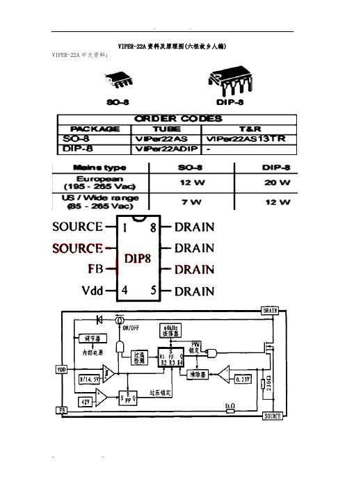
VIPER-22A资料及原理图(六祖故乡人编) VIPER-22A中文资料:黑表笔(脚)红表笔(脚)电阻(Ω)1、22、1 01、2 3 1.1k1、2 4 4.4k1、2 5、6、7、8 3.7k3 1、2 1.1k3 4 6.1k3 5、6、7、8 5.2k4 1、2 11k4 3 12.8k4 5、6、7、8 5k5、6、7、8 1、2 120k 5、6、7、8 3 125k 5、6、7、8 4 140kV IPER22A芯片概述:意法半导体的V IPER22A芯片为专用开关电源集成电路。
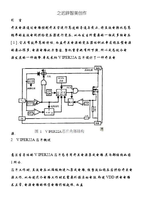
其部结构如图1所示。
芯片工作时, 直流电压从漏极脚进入集成电路, 经整流和稳压后供给开关电源工作, 从而使这个电路工作时不需要外接启动电阻。
即使VDD供电电路不正常, 电源电路的振荡电路仍能起振, 而且上图1 V IPER22A芯片部结构电路有输出电压。
在VDD正常前, 由芯片部自身供电, 经过很短时间后, VDD 供电电源正常, 此时,利用门电路控制开关电路(ON /OFF)断开从栅极输入的供电回路。
V IPER22A 有过热、过压保护功能。
VDD从4脚输入后, 首先送入比较器, 一旦输入VDD ≥42 V, 则触发器( FF1)输出一个置位信号1使控制振荡电路工作的触发器( FF2)输出为0,锁住U2 , 振荡信号无法输出, 即开关管不工作。
当输入电压小于1415 V时, U3 也将输出一个复位脉冲, 使开关管不工作。
当电路过热时, R1 为1,将FF2置0, 开关管不工作。
当供电电压VDD在正常围时, FB所得的取样电压与基准电压0123 V相比较, 用其比较结果去控制FF2 的转换频率,从而控制开关管的状态转换, 实现控制输出电压,达稳压的功能。
该集成电路芯片部包含60kHz的振荡电路, 其外围电路相当简单。
3 V IPER22A开关电源电路本文所使用的V IPER22A芯片具有优良的控制功能, 使得外围电路的设计较简单, 只需考虑一般的短路、过载电路保护即可。
AM22A高性能开关电源控制芯片功能描述AM22A芯片是专用小功率开关电源控制芯片,广泛用于电源适配器、LED电源、电磁炉、空调、DVD等小家电产品。
一、产品特点•采用双芯片设计,高压开关管采用双极型晶体管设计,以降低产品成本;控制电路采用大规模MOS数字电路设计,并采用E极驱动方式驱动双极型晶体芯片,以提高高压开关管的安全耐压值。
内建自供电电路,不需要外部给芯片提供电源,有效的降低外部元件的数量及成本。
•芯片内集成了高压恒流启动电路,无需外部加启动电阻。
•内置过流保护电路,防过载保护电路,输出短路保护电路,温度保护电路及光藕失效保护电路。
•内置斜坡补偿电路,保证在低电压及大功率输出时的电路稳定。
•内置PWM振荡电路,并设有抖频功能,保证了良好的EMC特性。
•内置变频功能,待机时自动降低工作频率,在满足欧洲绿色能源标准(<0.3W)同时,降低了输出电压的纹波。
•内置高压保护,当输入母线电压高于保护电压时,芯片将自动关闭并进行延时重启。
•内建斜坡电流驱动电路,降低了芯片的功耗并提高了电路的效率。
•4KV防静电ESD测试。
v1.6二、功率范围输入电压(85∼264V ac)(85∼145V ac)(180∼264V ac)最大输出功率12W18W18W三、封装与引脚定义引脚符号功能描述1Gnd接地引脚。
2Gnd接地引脚。
3Fb反馈控制端。
4Vcc供电引脚。
5678Collector输出引脚,连接芯片内高压开关管Collector端,与开关变压器相连。
四、内部电路框图五、极限参数供电电压Vcc...........................................-0.3V--9V供电电流Vcc...........................................100mA引脚电压...........................................-0.3V--Vcc+0.3V 开关管耐压...........................................-0.3V--780V峰值电流...........................................800mA总耗散功率...........................................1000mW工作温度...........................................0℃--125℃储存温度...........................................-55℃--+150℃焊接温度...........................................+280℃/5S六、电气参数项目测试条件最小典型最大单位电源电压Vcc AC输入85V-----265V456V启动电压AC输入85V-----265V 4.85 5.2V关闭电压AC输入85V-----265V 3.64 4.2V电源电流Vcc=5V,Fb=2.2V203040mA 启动时间AC输入85V------500mS Collector保护电压L=1.2mH460480500V开关管耐压Ioc=1mA700------V开关管电流Vcc=5V,Fb=1.6V----3.6V600650700mA 峰值电流保护Vcc=5V,Fb=1.6V----3.6V650720800mA 振荡频率Vcc=5V,Fb=1.6V----2.8V606570KHz 变频频率Vcc=4.6V,Fb=2.8V----3.6V0.5--65KHz 抖频步进频率Vcc=4.6V,Fb=1.6V----2.8V0.81 1.2KHz 温度保护Vcc=4.6V,Fb=1.6V----3.6V120125130℃占空比Vcc=4.6V,Fb=1.6V----3.6V5---50%控制电压Fb AC输入85V-----265V 1.6--- 3.6V七、工作原理•上电启动:当外部电源上电时,直流高压经开关变压器传至芯片的COLLECTOR端(5678引脚),后经内建高压恒流启动电路将启动电流送至开关管Q1的B极,通过开关管Q1的电流放大(约为20倍放大)进入电源管理电路经D1为Vcc外部电容C1充电,同时为Fb预提供一个3.6V电压(Fb引脚对地应接入一只滤波电容),当Vcc的电压逐步上升至5V时,振荡器起振,电路开始工作,控制器为Fb开启一个约为25uA的对地电流源,电路进入正常工作。
安森美快速充电解决方案详解
随着手机的屏幕越来越大,处理器的性能越来越强并升级多核。
为保证续航,手机的电池容量也变大,这样造成充电时间不可避免的变长。
如何缩短充电时间已成为手机应用的一大瓶颈。
相继出现基于不同厂商的快速充电解决方案,能够短暂的时间内有效提升充电效率。
点击了解车载多功能快速充电器方案,兼容所有安卓快充手机机型。
1. 方案框图
图示On Semi方案框图
2.方案特点
通过频率反走和跳周期模式,减少待机功耗
可通过光耦触发低功耗关闭模式
无损过功率补偿
基于定时器的过功率保护
输出短路保护
动态自供电的高压启动
欠压监测功能
有源X2 电容放电
严重故障时闩锁
自动恢复或闩锁选择的过流保护
空载待机能耗30 mW
可调功率过载保护
3.本解决方案主要芯片:
NCP1247是一个新的具有动态自供电功能的固定频率电流模式PWM控制器。
NCP1247应用实例框图。
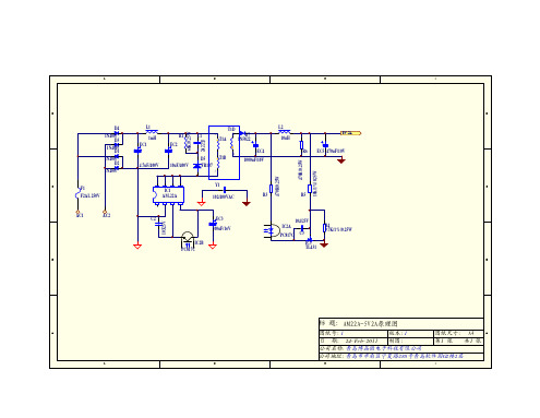
客户编号文件主管编号部门制表审核批准发布日期序号材料名称数量位号备注11/4W 电阻2R3,R621/4W 电阻1R41%31/4W 电阻1R51%41/4W 电阻1R15绦纶电容1C16瓷片电容1C27瓷片电容1C38高压瓷片电容1Y1P=10mm 9电解电容1EC3Φ5*11mm 10电解电容1EC5高频低阻Φ8*13mm 11电解电容1EC4高频低阻Φ8*15mm12高压电解电容1EC1Φ8*13mm 13高压电解电容1EC2Φ10*16mm14二极管4D1,D2,D3,D415二极管1D516二极管1D7DO-27塑封17IC 1IC118IC 1IC219IC 1IC320地环片1IC1的⑤⑦之间21AC 线2电源连接线L=40mm 红色 222A 带引脚保险管1FUSE1 套热缩管23工字电感1L1线径0.15mm 24工字电感1L2线径0.35mm 25变压器1T1EF20(5+5)26线路板180*41mm2011年2月23日1N40071000uF/10V 100uF/10VAM-22A TL4311mH(6*8)F2AL 250V 10uH(6*8)1N5822470R FR1074.7uF/400V 10uF/400V PC817C 24号线广州勇鑫电子有限公司内部BOM 清单-IM-CD1102-5V2A-AM22A主要材料供方规格型号第 1 版 第0 次修改共 1 页 第 1 页开发部ZL/ED-100119.7K 10K 68K 470uF/10V 2A223J 104/25V 102/400V 103/25V 测试要求高压测试:电源输入AC240V ,带线测试加2A 负载的电压范围为4.75-5.05V 。
低压测试:电源输入AC100V ,带线测试加2A 负载的电压范围为4.75-5.05V 。
之迟辟智美创作引言开关电源通过电路控制开关管进行高速的导通与截止, 将直流电转化为高频率的交流电提供给变压器进行变压, 从而发生所需要的一组或多组电压[ 1 ] .它具有效率高的特性, 而且开关电源的变压器体积比串连稳压型电源的要小很多, 电源电路比力整洁, 整机重量也有所下降, 所以成为现今电源发展的一种趋势.本文采纳V IPER22A芯片设计了一种开关电源.2V IPER22A芯片概述意法半导体的V IPER22A芯片为专用开关电源集成电路.其内部结构如图1所示.芯片工作时, 直流电压从漏极脚进入集成电路, 经整流和稳压后供给开关电源工作, 从而使这个电路工作时不需要外接启动电阻.即使VDD供电电路不正常, 电源电路的振荡电路仍能起振, 而且图1V IPER22A芯片内部结构电路有输出电压.在VDD正常前, 由芯片内部自身供电, 经过很短时间后, VDD供电电源正常, 此时,利用门电路控制开关电路(ON /OFF)断开从栅极输入的供电回路.V IPER22A 有过热、过压呵护功能.VDD从4脚输入后, 首先送入比力器, 一旦输入VDD ≥42 V, 则触发器( FF1)输出一个置位信号1使控制振荡电路工作的触发器( FF2)输出为0,锁住U2 , 振荡信号无法输出, 即开关管不工作.当输入电压小于1415 V时, U3 也将输出一个复位脉冲, 使开关管不工作.当电路过热时, R1 为1,将FF2置0, 开关管不工作.当供电电压VDD在正常范围时, FB所得的取样电压与基准电压0123 V相比力, 用其比力结果去控制FF2 的转换频率,从而控制开关管的状态转换, 实现控制输出电压,达稳压的功能.该集成电路芯片内部包括60kHz的振荡电路, 其外围电路相当简单.3V IPER22A开关电源电路本文所使用的V IPER22A芯片具有优良的控制功能, 使得外围电路的设计较简单, 只需考虑一般的短路、过载电路呵护即可.电路原理图如图2.图2电路原理图在交流电源的输入端接电容C0 用于滤除低频差模噪声, 接扼流圈用于过滤失落电网上的干扰, 同时也滤失落电源对电网的干扰.220 V的交流电源输入后, 经四个二极管构成的桥式整流电路整流, C1 滤波后输出一个300 V左右的直流信号.由于V IPER22A处于工作状态,在其内部场效应管截止时, 会在变压器低级两端发生年夜于300 V的电压, 利用R1、C2 和D5 构成防冲激电路, 使其电压有一个释放回路, 以免激穿V I2PER22A内部场效应管. 整流滤波后的直流电供给开关电源IC转换成高频的交流信号, 经变压器耦合输出各路低电压的交流信号.由于输入电压较高, 所以二极管的耐压值要很高, 而且电容的容量也要很年夜.互感发生的交流脉冲电压经D6 整流、R2限流和C3、C6 滤波后作为开关芯片的供电电压.由于V IPER22A的特殊结构, 如无VDD时可实现内部供电, 所以R2 即使击穿开路, 仍有电压输出, 但不正常.同时, VDD也为取样回路中的光耦的接收部份供电.另一部份电感感应到的脉冲电压经D8 整流, 又经电感L2、电容C12、C13、C14滤波后, 输出+ 5 V电压.+ 5 V电压同时经稳压管Z2 后给光耦电路发射部份供电, 通过光耦的接收部份接收到的光作为取样信号, 从V IPER22A的3脚FB输入到芯片, 从而去控制开关管的开关频率, 控制电源电压的稳定, 起到稳压的作用[ 2 ] .本电源电路由于前后级是通过光耦进行互相控制, 这样很好地隔离了前后级.同时, 变压器电感线圈另一端经D7整流C10滤波后输出+ 12 V的电压.变压器的一部份电感线圈经D10整流、C15滤波后输出 24 V电压.同时, 经R4 降压、 12 V稳压管Z1 稳压和C17滤波后输出12 V的电压.与+ 5 V电压输出一样, 变压器电感线圈输出的脉冲电压经D9 整流、电感L1、电容C16、C18、C19滤波后输出+ 9 V直流电压.4结束语本文设计的开关电源采纳V IPER22A 控制芯片, 由于它优异的性能, 使得控制电路在设计上比力简单.另外在电路的设计上直接对220 V的交流电压进行整流控制酿成高频的交流电压, 而没有采纳变压器降压后再控制, 这样就有效地减小了开关电源的体积.在交流输入端加入了扼流圈, 有效地将电网和电源隔离开来, 减小了互相的影响.输出电压采样使用了线形光耦采样, 将电源的输入和输出地线有效地进行了隔离, 也年夜年夜降低了地线反馈回路的影响, 从而抑制了电源输出的纹波.通过设计、制作和测试, 证明了按该思路研制出的开关电源是一种电路简单、可靠性高、实用价值强的支流稳压电源.。
VIPER-22A资料及原理图(六祖故乡人编) VIPER-22A中文资料:HR500-2型万能表R×1kΩ档估测的内阻值:黑表笔(脚)红表笔(脚)电阻(Ω)1、22、1 01、2 3 1.1k1、2 4 4.4k1、2 5、6、7、8 3.7k3 1、2 1.1k3 4 6.1k3 5、6、7、8 5.2k4 1、2 11k4 3 12.8k4 5、6、7、8 5k5、6、7、8 1、2 120k5、6、7、8 3 125k5、6、7、8 4 140kV IPER22A芯片概述:意法半导体的V IPER22A芯片为专用开关电源集成电路。
其内部结构如图1所示。
芯片工作时, 直流电压从漏极脚进入集成电路, 经整流和稳压后供给开关电源工作, 从而使这个电路工作时不需要外接启动电阻。
即使VDD供电电路不正常, 电源电路的振荡电路仍能起振, 而且上图1 V IPER22A芯片内部结构电路有输出电压。
在VDD正常前, 由芯片内部自身供电, 经过很短时间后, VDD供电电源正常, 此时,利用门电路控制开关电路(ON /OFF)断开从栅极输入的供电回路。
V IPER22A 有过热、过压保护功能。
VDD从4脚输入后, 首先送入比较器, 一旦输入VDD ≥42 V, 则触发器( FF1)输出一个置位信号1使控制振荡电路工作的触发器( FF2)输出为0,锁住U2 , 振荡信号无法输出, 即开关管不工作。
当输入电压小于1415 V时, U3 也将输出一个复位脉冲, 使开关管不工作。
当电路过热时, R1 为1,将FF2置0, 开关管不工作。
当供电电压VDD在正常范围时, FB所得的取样电压与基准电压0123 V相比较, 用其比较结果去控制FF2 的转换频率,从而控制开关管的状态转换, 实现控制输出电压,达稳压的功能。
该集成电路芯片内部包含60kHz的振荡电路, 其外围电路相当简单。
3 V IPER22A开关电源电路本文所使用的V IPER22A芯片具有优良的控制功能, 使得外围电路的设计较简单, 只需考虑一般的短路、过载电路保护即可。
XPM6320 (文件编号:S&CIC1465) 20W 快速充放电全集成电源管理芯片1 特性• 高至5A 开关模式降压充电- 4A 效率高至93%;5A 效率高至91% - 自适应5/9V 输入,支持FreeCharge TM 快速充电• 高至20W 同步Boost 升压放电92%- 兼容出电压• 符合 端口• - - • 待机/- - • - - 支持• Boost • • • 4颗• • 500K • 高精度- - - -• 高灵活度- 电阻可配置充电限流值 - 电阻可配置放电限流值 - 电阻可配置电量显示阈值- 电阻可配置电池内阻补偿,精确电量显示 - PIN 脚可配置电池类型 - PIN 脚可配置USB 端口类型XPM6320 (文件编号:S&CIC1465)20W快速充放电全集成电源管理芯片3概述XPM6320是一款集成度高,性能卓越,应用灵活的电源管理芯片,适用于锂离子电池和锂聚合物电池的充电管理和电源路径管理系统。
XPM6320集成电流模同步充电模块与升压模块,high-side/low-side开关采用20导通电阻NMOS,从而实现非常高的转换效率。
该芯片还集成了bootstrap diode为high-side开关的驱动电路供电。
同步整流控制环路包含有输入电压、输入电流,输出电压、输出恒流、温度平衡等五个环路,从而为XPM6320提供卓越的电源性能。
XPM6320可用外部电阻配置电池充电电流,最高可达5A。
其中,4A充电效率高至93%;5A充电效率高至91%。
Boost模块输出功率最高可达20W,5V/3A效率可达93%,9V/2A效率可达92%,12V/1.5A效率可达91%。
Boost模块具有输出电流恒流的功能,并可以通过外部电阻设置恒流值。
XPM6320内部集成了Quick Charge快充响应与快充请求协议,能够请求9V电压快速充电,从而节省电池的充电时间;也能够响应外接设备的快充请求,为外接设备传输更高的功率。
Integrated Charger/Boost Convertor with Power Path ControlFeaturesAdaptor Input Detection and Power Path Control Built-in 90m Ω Power Switch for Power Path ControlAdapter Input Over-Voltage ProtectionHigh Accuracy Switching Charger for 1 Cell Li-lon battery with Internal Compensation±0.5% Accuracy Battery Charger Output Voltage Charger Status Flag OutputAdapter Input Current Limit Controller with Built-in Current Sense ResistorTrickle Charging and Defective Battery Detec-tionHigh Efficiency Synchronous Boost Convertor Adjustable Output of Boost ConvertorEnable and Current Limit Control Pin for Boost Convertor.Output Short Circuit Protection for Boost Con-vertorAvailable for 4.2V/4.3V/4.35V Charge Voltage SettingAvailable for 2A/1.5A Charge CurrentSOP-8 (FD) PackageApplicationsMobile Battery BankGeneral DescriptionG5214 is an integrated charger/boost convertor with power path control for 1 cell Li-lon battery bank. The power path controller detects adapter input and control internal power switch of power path with over-voltage and over-current protection.The system operates in charger mode when adapter plug in. Charge current, battery voltage and adapter input current limit are regulated by constant off time buck controller with internal power MOSFET. The sys-tem enters trickle charge if battery voltage is too low. The charging stops if defective battery is detected. Charge Voltage has 2 options, 4.35V and 4.2V. Charge Current has 2 options, 2A and 1.5A. FLAG output indicates the charger status.The system operates in boost mode if adapter is absent and battery voltage is high enough. The output voltage is adjustable by external resistors with over current and short circuit protection. A 3-levels logic control the on/off and over-current of boost convertor.Ordering InformationORDER NUMBERMARKINGCHARGE CurrentCHARGE Voltage TEMP. RANGE PACKAGE (Green)G5214AF11U G5214A 2A 4.35V -40°C to +85°C SOP-8 (FD) G5214CF11U G5214C 2A 4.2V -40°C to +85°C SOP-8 (FD) G5214DF11U G5214D 1.5A 4.35V -40°C to +85°C SOP-8(FD) G5214FF11U G5214F 1.5A4.2V -40°C to +85°C SOP-8 (FD)Note: F1:SOP-8 (FD) 1: Bonding CodeU: Tape & ReelPin ConfigurationVADPVSYS EN/OCLX CSIP SOP-8 (FD)VBAT FLAGBTFB Note: Connect the thermal PAD to GND for proper function and excellent power dissipationAbsolute Maximum RatingsSupply Voltage (ADP to GND) . . . . . . . . .-0.3V to 6.5V Supply Voltage (ADP to GND, <30µS pulse ). . . . . . . . . . . . . . . . . . . . . . . . . . . . . . . . . . .-0.3V to 9V Supply Voltage (VSYS, VBAT to GND) . . . -0.3V to 6V CSIP to GND . . . . . . . . . . . . . . . . . . . . -0.3V to 6V LX to GND . . . . . . . . . . . . . . . . . . -0.5V to VSYS+0.5V Other Pins to GND. . . . . . . . . . . . . . . . . . . .-0.3V to 6V Thermal Resistance Junction to Ambient, (θJA )SOP-8 (FD) . . . . . . . . . . . . . . . . . . . . . . .132°C/W (1) SOP-8 (FD) (1in 2). . . . . . . . . . . . . . . . . . . . 108°C/W (2) Continuous Power Dissipation (T A = +25°C)SOP-8 (FD) . . . . . . . . . . . . . . . . . . . . . . .0.9W (1) SOP-8 (FD) (1in 2). . . . . . . . . . . . . . . . . . . . . . .1.2W (2) Thermal Resistance Junction to Case, (θJC )SOP-8 (FD) . . . . . . . . . . . . . . . . . . . . . . . . . . . 12°C/WStorage Temperature . . . . . . . . . . . . -65°C to +150°C Junction Temperature . . . . . . . . . . . . -10°C to +150°C Reflow Temperature (soldering, 10sec) . . . . . . .260°C ESD Protection (Human Body Mode) . . . . . . . . . . .2kVRecommended Operation ConditionsSupply Voltage (ADP to GND) . . . . . . . 4.8V to 5.5V Supply Voltage (VBAT to GND) . . . . . . .3V to 4.2V Operation Temperature (T A ) . . . . . . . -40°C to +85°CStress beyond those listed under “Absolute Maximum Ratings ” may cause permanent damage to the device.Note: (1): Please refer to Minimum Footprint PCB Layout Section. (2): Please refer to 1in 2 of 1oz PCB Layout Section.Electrical CharacteristicsADP =5V, V BAT =3.7V, T A =25°C, unless otherwise noted.The device is not guaranteed to function outside its operating conditions. Parameters with MIN and/or MAX limits are 100% tested at +25°C, unless otherwise specified.PARAMETER CONDITION MIN TYP MAX UNITSBattery Quiescent Current I VSYS =0 --- 500 700 µAVBAT=2.5V, Boost Convertor Stops --- 20 30 Battery Leakage CurrentVBAT=3.7V, Pull EN/OC low to shutdown--- 35 45 µAVBAT Rising2.62.752.9VBAT UVLO/ Trickle Charge ThresholdVBAT Falling 2.5 2.65 2.8VSwitch from VADP to VSYS --- 90 100m Ω Switch from VSYS to LX, V SYS =5V ---44 52 m Ω On-Resistance of Switches Switch from LX to GND, V SYS =5V --- 39 45 m Ω VSYS Short Circuit Blanking Time263443msVSYS Short Circuit Auto-Restart Time 177 238 300 msEN/OC input high threshold 4.5 --- ---EN/OC input low threshold --- --- 0.3 EN/OC Threshold EN/OC floating logic threshold 1.1 --- 3 V FLAG On Resistance ADP=5V---18 40 Ω FLAG Pin LeakageFLAG=6V--- 0.1 0.5 µA Thermal Shutdown Threshold Temperature Rising --- 150 --- °C Thermal Shutdown Hysteresis---25---°CAdapter Power Path Control ADP rising 4.65 4.74 4.83 V Adapter Power Good Threshold ADP falling 4.47 4.56 4.64 V ADP rising5.856.02 6.2 V Adapter OVP Threshold ADP falling 5.65 5.78 5.93 V G5214A/B/C, VSYS =0V 2.3 2.6 3.1Current Limit of Power SwitchG5214D/E/F, VSYS =0V1.82.1 2.6AElectrical Characteristics (continued)PARAMETER CONDITIONMINTYPMAX UNITSBOOST CONVERTORBTFB Output Voltage VBAT=3.0V~4.2V, I VSYS=0~2A 0.59 0.61 0.63VVSYS Short Current Limit VBAT>VSYS, R SNS=10mΩ, EN/OC floating 2.1 2.5 2.7 AReduction VSYS Short Current Limit VBAT>VSYS, R SNS=10mΩ, EN/OC input high 1.4 1.69 1.83 AVBAT=3.7V, EN/OC floating, R SNS=10mΩ 5.35 6.05 6.44VBAT=4.2V, EN/OC floating, R SNS=10mΩ 3.91 4.60 5.42Normal Inductor Peak Current LimitVBAT=3.0V, EN/OC floating, R SNS=10mΩ 5.42 6.40 7.49AVBAT=3.7V, EN/OC input high, R SNS=10mΩ 4.30 4.80 5.10VBAT=4.2V, EN/OC input high, R SNS=10mΩ 3.35 3.75 4.25Reduction Inductor Peak Current LimitVBAT=3.0V, EN/OC input high, R SNS=10mΩ 4.36 5.10 6.00AVBAT= 3.7V 1.2471.4341.649VBAT= 4.2V 1.421.6321.877Off-TimeVBAT=3V 1.0211.1641.339µsMinimum Off-Time --- 250 --- nsBoost Convertor OVP Threshold VSYS rising, reference to the normal boostoutput5 8 11 %Current Threshold of Asynchronous Converting R SNS=10mΩ100 150 300mASoft Start Time VBAT=3.7V, VSYS Rising to 4.8V --- 1 --- msBattery ChargerG5214C/F 4.1794.24.221Battery Charge Voltage AccuracyG5214A/D 4.328 4.35 4.372VG5214A/C, RSNS=10mΩ 1.83 2 2.17Charge Current AccuracyG5214D/F, RSNS=10mΩ 1.37 1.5 1.63AG5214A/C, RSNS=10mΩ110 250 350Trickle Charge Current AccuracyG5214D/F, RSNS=10mΩ80 200 300mAG5214A/C 1.822.3 Adapter Current Limit AccuracyG5214D/F 1.31.51.8AVSYS=5V, VBAT=3.7V 0.543 0.621 0.714VSYS=5V, VBAT=4.2V 0.329 0.379 0.436Off-TimeVSYS=5V, VBAT=2V 1.243 1.429 1.643µsMinimum Off-Time --- 250 --- nsDead Battery Detection Timeout Period 15415 17728 20387SVBAT rising, reference to the charge voltage 3.88 4 4.12Battery OVP ThresholdVBAT falling, reference to the charge voltage 2.43 2.5 2.58%Current Threshold of Asynchronous Converting R SNS=10mΩ-100 146 270mAMinimum Footprint PCB Layout SectionSOP-8 (FD)1in of 1oz PCB Layout SectionSOP-8 (FD)PIN NAMEPIN FUNCTION1 EN/OC Leave the pin floating set normal operating of boost convertor. Connect this pin to VBAT setthe current limit of boost convertor to 3/4 of normal value. Connect this pin to GND to shutdown the boost convertor.2 LX Connect the pin to output inductor.3 VSYS System output. Connect 33µFX2 capacitors to GND. 4VADPAC adapter input. Connect a capacitor to GND.5 FLAGCharger status indicator, open-drain output. The output is pulled low if the system is in charg-ing mode and battery is not fully charged. 6 BTFB Connect 2 resistors in series from VSYS to BTFB to GND to set the boost output votage 7 VBAT Battery input. Connect 20µF capacitors to GND. 8CSIPCurrent detection input.9 GND GroundBlock DiagramFunction DescriptionG5214 detects the plug-in of adapter, turns on power switch and decides boost/charging mode of the sys-tem automatically. If adapter is absent and battery voltage is high enough, the power switch is turned off and G5214 is in boost mode, the boost converter out-puts to system output source from battery. The power switch is turned on after adapter is plugged-in and detected. G5214 turns into charger mode after the power switch is fully turned on. In charger mode, sys-tem output is directly supply from adapter via the power switch, and the charger convertor supply charging current to the battery from system output. There are several protections of power path, boost convertor and charger convertor.Power Path ControlAdapter is detected if VADP is larger than power good threshold (4.74V with hysteresis) and smaller than OVP threshold (5.78V with hysteresis). After the de-tection of adapter, the power switch between VSYS and VADP turns on. The gate of NMOS switch rises slowly to minimize surge current of adapter. There is over-current protection for the power switch. If over-load occurs on VSYS, the switch gate is lowered down to keep the current flow through the switch in current limit to protect adapter and the switch.When adapter input OVP is detected, the power switch is shutdown immediately to keep VSYS below normal voltage range to protect the devices connected to VSYS from damaged by high voltage.After the gate of power switch rises high enough and no abnormal event is detected. The system gets into charger mode. If system isn’t in charger mode and the battery voltage is higher than VBAT UVLO threshold, the system operates in boost mode, otherwise the system is shutdown.Boost ConvertorIn boost mode, VSYS is boosted to the voltage setting by external resistors connected from VSYS to BTFB to GND. The BTFB pin is regulated to 0.61V. The con-troller of boost is constant off-time and the off-time is calculated by VSYS and VBAT to keep the switching frequency near 500kHz. Internal soft-start controls the rising time of VSYS output to about 1ms. There is OVP function of boost output.Boost convertor has current limit functions. If VSYS is lower than VBAT, the inductor current is limited to 2.5A. If VSYS is larger than VBAT, G5214 performs cycle by cycle peak inductor current limit. The current limit value is inversely proportion to VBAT, that makes output current limit changes slightly versus battery voltage.EN/OC pin controls the operation of boost convertor. The current limit is set to 3/4 of normal value when EN/OC is connected to VBAT. The boost convertor is shut down if EN/OC pin is pulled to GND. Leave the pin floating for normal operation.Charger ConvertorIn charger mode, adapter is connected to VSYS as the power of charger for 1 cell Li-lon battery. The system controls the battery voltage to 4.35V, 4.3V or 4.2V for G5214A/G5214D and G5214CG5214F, respectively. The charging current is lower down if adapter current is larger than a preset level. The current limit of total adapter current is 2A or 1.5A and current is sensed by internal resistor. The controller is constant off-time and the off-time is calculated by VSYS and VBAT to keep the switching frequency near 700kHz. The charger convertor is internal compensated.If battery voltage is below the UVLO threshold, the system is trickle charged with 15% of the normal charging current. The battery is determined as dead battery if battery voltage keeps under the UVLO threshold for over 17728S.G5214 has over-voltage protection for charger. The high and low side switched are turned off immediately if battery voltage goes over 4% of normal battery volt-age setting.The charge current is 2A or 1.5A. The adapter current is also limited to 2A or 1.5A. The current limits of power switch is 2.6A or 2.1A.Over-Current ProtectionsThe over-current protection of VSYS pin is auto-restart mode. If any of VSYS OCP event occurs (OCP of power switch or boost convertor) and lasting over 34ms, the system shutdown for 238ms and re-start again. The function keep the system temperature low even if VSYS is short. G5214 also have over-temperature protection. The whole system is shutdown if temperature rises over 150°C.Charger Status FlagWhen G5214 operates in charging mode, FLAG out-puts low if the battery is not fully charged. The FLAG pin outputs high impedance if system is not in charg-ing or the battery is fully charged.Application InformationInductor SelectionInductance between 3.3µH and 10µH is recommended. The RHZ is lower with large inductance. Select smaller inductance with larger VSYS capacitance to enlarge system bandwidth with the same output ripples at boost mode. It’s important to select inductor with maximum current to avoid saturation. Check both charger mode and boost mode for peak current.VSYS Capacitor SelectionThe recommended value of this capacitors is 33µFX2. This value maintain the boost controller loop at proper bandwidth with sufficient phase margin.VBAT Capacitor SelectionConnect 20µF capacitor to maintain charger loop sta-bility and serve as input capacitor at boost mode. Current Sense Resistor SelectionThe charging current and current limit at boost mode are inverse proportion to R SNS. Select 10mΩR SNS for proper current setting. To maintain stability of charger loop, 10mΩ or larger R SNS is recommanded.PCB Layout ConsiderationsSignal Ground and Power Ground ConnectionAt minimum, a reasonably large area of copper, which will shield other noise couplings through the IC, should be used as signal ground beneath the IC. The best tie-point between the signal ground and the power ground is at the negative side of the output capacitor on each side, where there is little noise; a noisy trace beneath the IC is not recommended.LX PinThis trace should be short, and positioned away from other weak signal traces. This node is noisy and has high voltage swing. No trace should be in parallel with it.CSIP, VBAT PinsThese pins is used as the battery voltage and inductor current feedback. The traces should be away from the noisy pins like LX. In general, the current sense resis-tor R SNS should be close to the IC.Copper Size for the LX NodeThe capacitance of LX should be kept very low to minimize ringing. It would be best to limit the size of the LX node copper.Exposed PADIt’s highly recommended to add larger copper to ex-posed PAD connected to signal ground. At high cur-rent operation, the power consumption is high. Large copper to exposed PAD decrease thermal resistance much.Package InformationSOP- 8 (FD) PackageTaping SpecificationPACKAGE Q ’TY/REELSOP-8 (FD)2,500 eaGMT Inc. does not assume any responsibility for use of any circuitry described, no circuit patent licenses are implied and GMT Inc. reserves the right at any time without notice to change said circuitry and specifications.。