
chip synthesis芯片综合
- 格式:ppt
- 大小:2.67 MB
- 文档页数:101
北京工业大学硕士学位论文集成电路物理设计中布局和电源网络的设计姓名:朱延洲申请学位级别:硕士专业:嵌入式系统指导教师:林平分;于忠臣20070401第2章布局和f乜源阀耋名设计概述第2章布局和电源网络设计概述2.1集成电路设计流程集成电路的设计过程如图2.1所示。
集成电路也叫芯片(Chip),从最初的需求到生成最终的芯片要经历几个步骤,首先是研究(StudyPhase)阶段,对于芯片进行研究,并给出一个详细的芯片设计规范(ChipSpec)。
前端(FrontEnd)拿到芯片的设计规范(ChipSpee)以后进行功能设计和仿真(FunctionalDesign&Simulation),此步是按照设计规范将芯片的功能用硬件描述语言(HardwareDescriptiOilLanguage,HDL)来实现出来,并且通过仿真来验证芯片的功能,此步完成以后会生成一个寄存器晶体管级的代码(RegisterTransistorLevelCode,RTLCode)。
之后再经过综合(Synthesis)将RTL代码综合生成门级网表(Gate-levelNetlist),然后再将门级网表和约束(Contrains)交给后端(BackEnd)来完成芯片的物理设计(PhysicalDesign)。
芯片的物理设计是将门级网表实现成为可以流片(Tapeout)的GDSII版图,之后再将GDSII文件送到晶元厂去流片,流片后再送到封装厂进行封装(Package),之后就生产出了我们所见到的芯片了。
图2-1集成电路设计流程}Cdesi卵f}w由这个流程我们可以看出,物理设计是整个芯片设计的最后一步,其中包含北京r:业凡学T挥碗l。
学位论义金属的密度。
11)物理验证(PhysicalVerification:DRC&LVS)。
DRC是对芯片版图中的各层物理图形进行设计规则检查,它也包括天线效应的检查,以确保芯片流片成功。
LVS主要是将版图和电路的网表进行比较,来保证流片出来的版图电路和实际需要的电路一致。
第一节,综合举例什么是综合呢?synthesis,台湾翻译为-合成,其作用就是将硬件描述语言的RTL级代码转变为门级网表。
当然,现在综合技术已经很成熟了,还有推出的行为(behavioral)综合和物理(physical)综合。
我们这里讨论的是逻辑(logic)综合。
综合技术是提高设计产能的一个很重要的技术,没有综合技术的发展,我们就不可能用HDL实现电路的设计,因为HDL开始是用来供电路仿真建模使用的,到了后来才把其中一部分子集作为可综合的语言,也就是我们使用的RTL CODE。
很多人入门都用HDL做设计,就以为HDL就只是用来做设计的,没有看到HDL最初始的一面,所以在验证的时候,就无法用好HDL另外一部分强大的功能。
有时间还是可以看看Writing Testbench这本书,增强对HDL语言在验证方面作用的了解,也是提高对HDL认识很好的补充。
我们以DesignCompiler为例子讲解综合的过程。
首先,综合就要必须要用综合库,这个你可以向厂家要,综合库可以通过.lib这个库文件转变成.db综合库,这个过程可以在DesignCompiler里面用实现,综合库里面有什么内容呢?.db 是无法阅读的,.lib是可以阅读的,里面有库的基本参数的单位,库运行的条件,各种参数,最重要的是两个部分,一个是WLM-Wire Load Model,一个Gate的定义(输入输出,功能,时序参数,面积等等);这只是StandarCell的库,另外还有其他库,如RAM,DSP的综合库,都以.db的形式存在。
综合需要三种输入,一个是代码,一个是综合库,一个是综合脚本Script。
综合脚本主要包括了一下内容,对综合工具环境的配置,对综合对象外部环境的设置(operation condiction),对WLD的设置,对综合对象的时序的约束,综合策略,综合优化,综合报告和输出。
下面给入门的人一个现成的Script 例子。
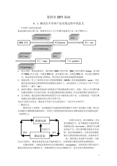
第四章 DFT 基础4.1 测试在半导体产品实现过程中的意义一 半导体产品的实现过程集成电路从设计到产品一般要经历以下几个步骤才能成为产品(如下图所示):verilog ,也可能用VHDL 语言写成,可能是RTL 级,也可能是门级。
如果是RTL 级,首先进行逻辑综合、验证将设计转变成门级网表,然后进行布局布线变成最终的版图。
2. 制造过程:代工厂接受来自设计者的版图数据(GDSII )将其制成掩膜版(mask ),然后通过复杂的制造过程将期望的电路做在晶园片上,这时晶园片上已经包含了若干个芯片的原型--裸片(die )。
3. 晶园片测试:制造好的晶园片需要进行严格的测试然后划片、封装,实际上只有那些通过测试的裸片才会进行封装,而未通过测试的裸片被淘汰。
经过封装的裸片就变成芯片。
4. 芯片测试:通过晶园片测试和封装的芯片还不能算真正的产品,它仍然要进一步进行测试确认没有故障才能成为真正的半导体产品。
从这个过程可以看出,测试是半导体产品实现过程中一个必不可少的环节。
二 测试定义测试实际上是指将一定的激励信号加载到需要检测的半导体产品的输入引脚,然后在它的输出引脚检测电路的响应,并将它与期望的响应相比较以判断电路是否有故障的过程(如图所示)。
在这个过程中,测试设备要发出适当的控制信号,式(test pattern ),这两者的主要区别在于测试向量仅仅包含激励信号,而测试模式不仅包含激励信号,而且还包含期望的响应。
由图可以看出,要实现测试,首先要有激励信号,这个激励信号就是所谓的测试向量(test vector )。
激励信号由测试设备产生;然后要判断电路是否有故障,就必须检测响应,并将实际检测的响应与期望的响应相比较,如果两者不一致,我们就认为电路中有故障。
当然以使得整个测试过程得以顺利进行。
在测试领域,与测试向量相对应还有测试模由上面的分析可以看出,测试问题在测试前就是测试模式生成和测试模式验证(时序验证)问题;而在测试时就是测试向量施加和测试响应检测及结果判断问题。

asic设计及验证流程英文回答:ASIC Design and Verification Process.ASIC stands for Application Specific Integrated Circuit, which is a custom designed semiconductor chip that is designed for a specific use. The ASIC design andverification process involves several stages, each of which is critical for ensuring the correct functionality and performance of the chip.1. System Specification and Definition.The first stage of the ASIC design process involves defining the requirements and specifications of the system that will be implemented on the chip. This includes identifying the input and output signals, the data processing algorithms, and the performance requirements.2. Architectural Design.Based on the system specification, an architectural design is developed. The architectural design defines the overall structure of the chip, including the different modules and their interconnections. The architecturaldesign is typically captured using a hardware description language (HDL), such as Verilog or VHDL.3. RTL Design.The architectural design is then converted into a register-transfer level (RTL) design. The RTL design is a more detailed representation of the chip's functionality, including the logic gates and flip-flops. The RTL design is also captured using an HDL.4. Simulation.The RTL design is simulated to verify its functionality. Simulation involves applying input stimuli to the designand checking the outputs to ensure that they are correct.Simulation can be performed using a variety of software tools.5. Synthesis.The RTL design is then synthesized into a gate-level netlist. The gate-level netlist is a detailed representation of the chip's layout, including the placement and routing of the transistors.6. Physical Design.The gate-level netlist is then used to create a physical design of the chip. The physical design includes the placement of the transistors, the routing of the wires, and the layout of the pads.7. Fabrication.The physical design is then sent to a fabrication facility to be manufactured. The fabrication process involves creating the transistors and wiring on the chip.8. Verification.After fabrication, the chip is tested to verify its functionality. Verification involves applying input stimuli to the chip and checking the outputs to ensure that they are correct. Verification can be performed using a variety of techniques, including functional testing and structural testing.9. Packaging and Shipping.The verified chip is then packaged and shipped to the customer. The packaging process includes assembling the chip into a package, such as a plastic or ceramic package.中文回答:ASIC设计和验证流程。