
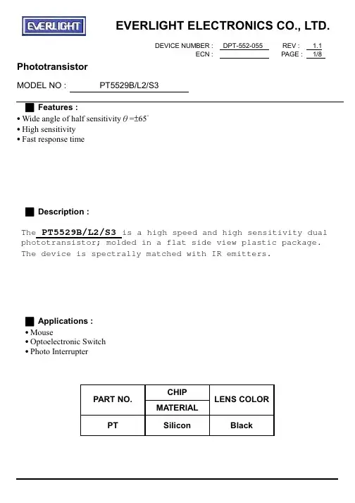
PT55928BL2中文资料
- 格式:pdf
- 大小:249.54 KB
- 文档页数:8

.描述PT2258是一个6通道电子音量控制器IC,采用CMOS集成电路技术专门设计的新一代A V多声道音频系统。
2258提供I2C控制接口,0到-79db的衰减范围在1 db /一步,低噪声,高通道分离。
采用20引脚DIP、SOP,,PT2258的引脚分配和应用电路进行了优化,便于PCB布局和节省成本的优势。
特征·CMOS技术·低功耗·最少外部元件·衰减范围:0 - -79db在1 db /步·工作电压:5 - 9 V·噪音低、信噪比> 100分贝(A-weighting)·高通道分离·I2C总线控制接口·可选地址·6通道输出·20引脚DIP或SOP应用·AV环绕音响设备·汽车音响·Mini Compo·计算机多媒体扬声器·其他音响设备'..结构图'..引脚排列引脚说明引脚名称I/O 描述引脚号1 1号。
连接一个电容到音频源IN1 I 通道输入2 号。
连接一个电容到音频源I 通道输入2IN23 I 通道输入IN3 3号。
连接一个电容到音频源4 参考地址代码段CODE2 --5 数字地DGND --6 时钟输入SCL I I2C7 I I2C数据输入SDA8 4I IN4 号。
连接一个电容到音频源通道输入9 号。
连接一个电容到音频源IN5 I 通道输入510 通道输入6IN6 I 号。
连接一个电容到音频源11 号连接一个电容器到下一个阶段通道输出6OUT6 O12 通道输出5号连接一个电容器到下一个阶段OUT5 O13 通道输出OUT4 O 4号连接一个电容器到下一个阶段14 14-- GND 地(脚)15 REF --= 1 / 2VCC参考电压连接一个电容到地上16 VCC -- 16电源输入(脚)17 -- CODE1 参考地址代码段18 3通道输出O 号连接一个电容器到下一个阶段OUT319 2通道输出号连接一个电容器到下一个阶段O OUT220号连接一个电容器到下一个阶段OUT11通道输出O'..功能描述总线接口数据传输是通过微处理器PT2258 的SDA和SCL。
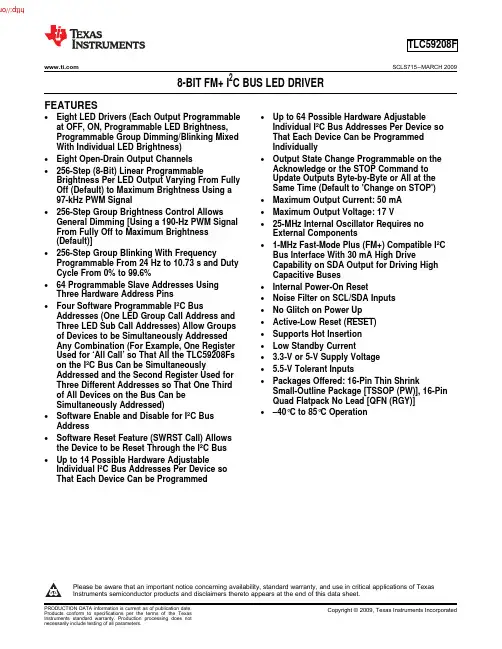
FEATURESTLC59208F SCLS715–MARCH 20098-BIT FM+I 2C BUS LED DRIVER•Eight LED Drivers (Each Output Programmable •Up to 64Possible Hardware Adjustableat OFF,ON,Programmable LED Brightness,Individual I 2C Bus Addresses Per Device so Programmable Group Dimming/Blinking Mixed That Each Device Can be Programmed With Individual LED Brightness)Individually•Eight Open-Drain Output Channels •Output State Change Programmable on the Acknowledge or the STOP Command to •256-Step (8-Bit)Linear ProgrammableUpdate Outputs Byte-by-Byte or All at the Brightness Per LED Output Varying From Fully Same Time (Default to 'Change on STOP')Off (Default)to Maximum Brightness Using a 97-kHz PWM Signal•Maximum Output Current:50mA •256-Step Group Brightness Control Allows •Maximum Output Voltage:17VGeneral Dimming [Using a 190-Hz PWM Signal •25-MHz Internal Oscillator Requires no From Fully Off to Maximum Brightness External Components(Default)]•1-MHz Fast-Mode Plus (FM+)Compatible I 2C •256-Step Group Blinking With FrequencyBus Interface With 30mA High DriveProgrammable From 24Hz to 10.73s and Duty Capability on SDA Output for Driving High Cycle From 0%to 99.6%Capacitive Buses•64Programmable Slave Addresses Using •Internal Power-On ResetThree Hardware Address Pins•Noise Filter on SCL/SDA Inputs •Four Software Programmable I 2C Bus•No Glitch on Power Up Addresses (One LED Group Call Address and •Active-Low Reset (RESET)Three LED Sub Call Addresses)Allow Groups •Supports Hot Insertion of Devices to be Simultaneously Addressed Any Combination (For Example,One Register •Low Standby CurrentUsed for ‘All Call’so That All the TLC59208Fs • 3.3-V or 5-V Supply Voltage on the I 2C Bus Can be Simultaneously• 5.5-V Tolerant InputsAddressed and the Second Register Used for •Packages Offered:16-Pin Thin ShrinkThree Different Addresses so That One Third Small-Outline Package [TSSOP (PW)],16-Pin of All Devices on the Bus Can be Quad Flatpack No Lead [QFN (RGY)]Simultaneously Addressed)•–40°C to 85°C Operation•Software Enable and Disable for I 2C Bus Address•Software Reset Feature (SWRST Call)Allows the Device to be Reset Through the I 2C Bus •Up to 14Possible Hardware AdjustableIndividual I 2C Bus Addresses Per Device so That Each Device Can be ProgrammedPlease be aware that an important notice concerning availability,standard warranty,and use in critical applications of Texas Instruments semiconductor products and disclaimers thereto appears at the end of this data sheet.PRODUCTION DATA information is current as of publication date.Copyright ©2009,Texas Instruments IncorporatedProducts conform to specifications per the terms of the Texas Instruments standard warranty.Production processing does not necessarily include testing of all parameters.11621531441351261171089V CC SDA SCL RESET OUT7OUT6OUT5OUT4A0A1A2OUT0OUT1GNDOUT2OUT3116215314413512611710SDA SCL RESET OUT7OUT6OUT5V CCA0A1A2OUT1OUT0OUT3OUT289OUT4GND DESCRIPTIONTLC59208FSCLS715–MARCH PW PACKAGE RGY PACKAGE (TOP VIEW)(TOP VIEW)The TLC59208F is an I 2C bus controlled 8-bit LED driver optimized for red/green/blue/amber (RGBA)color mixing applications.Each LED output has its own 8-bit resolution (256steps)fixed frequency individual PWM controller that operates at 97kHz with a duty cycle that is adjustable from 0%to 99.6%to allow the LED to be set to a specific brightness value.An additional 8-bit resolution (256steps)group PWM controller has both a fixed frequency of 190Hz and an adjustable frequency between 24Hz to once every 10.73seconds with a duty cycle that is adjustable from 0%to 99.6%that is used to either dim or blink all LEDs with the same value.Each LED output can be off,on (no PWM control),set at its individual PWM controller value or at both individual and group PWM controller values.The TLC59208F operates with a supply voltage range of 3V to 5.5V and the outputs are 17V tolerant.LEDs can be directly connected to the TLC59208F device outputs.Software programmable LED Group and three Sub Call I 2C bus addresses allow all or defined groups of TLC59208F devices to respond to a common I 2C bus address,allowing for example,all the same color LEDs to be turned on or off at the same time or marquee chasing effect,thus minimizing I 2C bus commands.Three hardware address pins allow up to 64devices on the same bus (see Table 1).The software reset (SWRST)Call allows the master to perform a reset of the TLC59208F through the I 2C bus,identical to the power-on reset (POR)that initializes the registers to their default state causing the outputs to be set high (LED off).This allows an easy and quick way to reconfigure all device registers to the same condition.ORDERING INFORMATION (1)T APACKAGE (2)ORDERABLE PART NUMBER TOP-SIDE MARKING QFN –RGY Reel of 2500TLC59208FIRGYR Y59208F –40°C to 85°C TSSOP –PWReel of 2000TLC59208FIPWRY59208F(1)For the most current package and ordering information,see the Package Option Addendum at the end of this document,or see the TI web site at .(2)Package drawings,thermal data,and symbolization are available at /packaging .2Submit Documentation FeedbackCopyright ©2009,Texas Instruments IncorporatedProduct Folder Link(s):TLC59208FTLC59208F SCLS715–MARCH 2009BLOCK DIAGRAMNOTE:Only one PWM shown for clarity.TERMINAL FUNCTIONSTERMINAL I/O (1)DESCRIPTIONNAME NO.A01I Address input 0A12I Address input 1A23I Address input 2OUT0,OUT1,4,5,OUT2,OUT3,6,7,O Open-drain output 0to 7,LED ON at low OUT4,OUT6,9,10,OUT6,OUT711,12GND 8–GroundRESET 13I Active-low reset input SCL 14I Serial clock input SDA 15I/O Serial data input/output V CC16–Power supply(1)I =input,O =outputCopyright ©2009,Texas Instruments Incorporated Submit Documentation Feedback3Product Folder Link(s):TLC59208FABSOLUTE MAXIMUM RATINGS (1)RECOMMENDED OPERATING CONDITIONS (1)TLC59208FSCLS715–MARCH over operating free-air temperature range (unless otherwise noted)MINMAXUNIT V CC Supply voltage range 07V V I Input voltage range –0.47V V O Output voltage range –0.520V I O Continuous output current 50mA PW package (2)108θJA Package thermal impedance°C/W RGY package (3)39PW package 0.90P D Power Dissipation,T A =25°C,JESD 51-7W RGY package2.08T J Junction temperature range –40150°C T stg Storage temperature range–55150°C(1)Stresses beyond those listed under "absolute maximum ratings"may cause permanent damage to the device.These are stress ratings only,and functional operation of the device at these or any other conditions beyond those indicated under "recommended operating conditions"is not implied.Exposure to absolute-maximum-rated conditions for extended periods may affect device reliability.(2)The package thermal impedance is calculated in accordance with JESD 51-7.(3)The package thermal impedance is calculated in accordance with JESD 51-5.TEST CONDITIONSMIN MAX UNIT V CC Supply voltage 35.5V V IH High-level input voltage SCL,SDA,RESET,A0,A1,A20.7×V CC5.5V V IL Low-level input voltage SCL,SDA,RESET,A0,A1,A200.3×V CCV V O Output voltageOUT0to OUT717V V CC =3V 20I OL Low-level output current SDAmA V CC =4.5V30I O Output currentOUT0to OUT750mA T A Operating free-air temperature–4085°C(1)All unused inputs of the device must be held at V CC or GND to ensure proper device operation.4Submit Documentation FeedbackCopyright ©2009,Texas Instruments IncorporatedProduct Folder Link(s):TLC59208FELECTRICAL CHARACTERISTICS TLC59208F SCLS715–MARCH2009V CC=3V to5.5V,T A=–40°C to85°C(unless otherwise noted)PARAMETER TEST CONDITIONS MIN TYP(1)MAX UNITSCL,SDA,A0,Input/output leakageI I A1,A2,V I=V CC or GND±0.3µAcurrentRESETOutput leakageOUT0to OUT7V O=17V,T J=25°C0.5µA currentV POR Power-on reset voltage 2.5VV CC=3V,V OL=0.4V20Low-level outputI OL SDA mAcurrent VCC=4.5V,V OL=0.4V30V CC=3V,I OL=50mA108185 Low-level outputV OL OUT0to OUT7mV voltage VCC=4.5V,I OL=50mA90165V CC=3V,I OL=50mA2 3.75r ON ON-state resistance OUT0to OUT7ΩV CC=4.5V,I OL=50mA 1.8 3.3T SD Thermal shutdown temperature(2)150175200°CT HYS Restart hysteresis15°CSCL,A0,A1,C i Input capacitance V I=V CC or GND6pFA2,RESETInput/outputC io SDA V I=V CC or GND8pFcapacitanceV CC=3.3V,OUT0to OUT7=OFF5I CC Supply current mAV CC=5.5V,OUT0to OUT7=OFF8(1)All typical values are at T J=25°C.(2)Specified by design,not production tested.Copyright©2009,Texas Instruments Incorporated Submit Documentation Feedback5Product Folder Link(s):TLC59208FI 2C INTERFACE TIMING REQUIREMENTSTLC59208FSCLS715–MARCH T A =–40°C to 85°CSTANDARD-MODEFAST-MODE FAST-MODE PLUSI 2C BUSI 2C BUS I 2C BUSUNITMINMAX MIN MAX MIN MAX I 2C Interface f SCL SCL clock frequency0100040001000kHz I 2C bus free time between stop and t BUF 4.7 1.30.5µs startt HD;STA Hold time (repeated)Start condition 40.60.26µs Set-up time for a repeated Start t SU;STA 4.70.60.26µs conditiont SU;STO Set-up time for Stop condition 40.60.26µs t HD;DAT Data hold time00ns t VD;ACK Data valid acknowledge time (1)0.3 3.450.10.90.050.45µs t VD;DAT Data valid time(2)0.3 3.450.10.90.050.45µs t SU;DAT Data set-up time25010050ns t LOW Low period of the SCL clock 4.7 1.30.5µs t HIGH High period of the SCL clock 40.60.26µs Fall time of both SDA and SCL t f 30020+0.1C b (5)300120ns signals (3)(4)Rise time of both SDA and SCL t r 100020+0.1C b (5)300120ns signalsPulse width of spikes that must be t SP 505050nssuppressed by the input filter (6)Reset t W Reset pulse width 101010ns t REC Reset recovery time 000ns t RESET Time to reset (7)(8)400400400ns(1)t VD;ACK =time for Acknowledgement signal from SCL low to SDA (out)low.(2)t VD;DAT =minimum time for SDA data out to be valid following SCL low.(3)A master device must internally provide a hold time of at least 300ns for the SDA signal (refer to the VIL of the SCL signal)in order to bridge the undefined region of SCLs falling edge.(4)The maximum tf for the SDA and SCL bus lines is specified at 300ns.The maximum fall time (t f )for the SDA output stage is specified at 250ns.This allows series protection resistors to be connected between the SDA and the SCL pins and the SDA/SCL bus lines without exceeding the maximum specified t f .(5)C b =total capacitance of one bus line in pF.(6)Input filters on the SDA and SCL inputs suppress noise spikes less than 50ns(7)Resetting the device while actively communicating on the bus may cause glitches or errant Stop conditions.(8)Upon reset,the full delay will be the sum of t RESET and the RC time constant of the SDA bus.6Submit Documentation FeedbackCopyright ©2009,Texas Instruments IncorporatedProduct Folder Link(s):TLC59208FPARAMETER MEASUREMENT INFORMATIONSDASCLSTARTACK OR READ CYCLERESETOUTnProtocolStart Condition (S)Bit 7MSB (A7)Bit 6(A6)Bit 7(D1)Bit 8(D0)Acknowledge(A)Stop Condition (P)SCLSDAt t HD;ST ASU;DA T HD;DA T VD;DA T VD;ACK SU;STOTLC59208F SCLS715–MARCH 2009Figure 1.Definition of RESET TimingFigure 2.Definition of TimingNOTE:Rise and fall times refer to V IL and V IH .Figure 3.I 2C Bus TimingCopyright ©2009,Texas Instruments Incorporated Submit Documentation Feedback7Product Folder Link(s):TLC59208FV DDOpenGNDTLC59208FSCLS715– PARAMETER MEASUREMENT INFORMATION(continued)NOTE:R L=Load resistance for SDA and SCL;should be>1kΩat3-mA or lower current.C L=Load capacitance;includes jig and probe capacitance.R T=Termination resistance;should be equal to the output impedance(Z O)of the pulse generator.Figure4.Test Circuit for Switching Characteristics8Submit Documentation Feedback Copyright©2009,Texas Instruments IncorporatedProduct Folder Link(s):TLC59208FAPPLICATION INFORMATION Functional DescriptionDevice AddressRegular I2C Bus Slave AddressTLC59208F SCLS715–MARCH2009Following a Start condition,the bus master must output the address of the slave it is accessing.The I2C bus slave address of the TLC59208F is shown in Figure5.Slave address pins A0,A1,and A2choose1 of64slave addresses.To conserve power,no internal pullup resistors are incorporated on A0,A1,or A2. Address values,depending on A0,A1,and A2,can be found in Table1.NOTE:When using the TLC59208F,reserved I2C bus addresses must be used with cautionsince they can interfere with the following:•"Reserved for future use"I2C bus addresses(0000011,1111101,1111110,1111111)•Slave devices that use the10-bit addressing scheme(11110xx)•High-speed mode master code(00001xx)Figure5.Slave AddressThe last bit of the address byte defines the operation to be performed.When set to logic1,a read operation is selected.When set to logic0,a write operation is selected.Regular I2C Bus Slave AddressTable1.TLC59208F Address MapADDRESS INPUT SLAVE ADDRESSA2A1A0A6A5A4A3A2A1A0ADDRESS GND SCL GND001000020h GND SCL V CC001000122h GND SDA GND001001024h GND SDA V CC001001126h V CC SCL GND001010028h V CC SCL V CC00101012Ah V CC SDA GND00101102Ch V CC SDA V CC00101112Eh GND SCL SCL001100030h GND SCL SDA001100132h GND SDA SCL001101034h GND SDA SDA001101136h V CC SCL SCL001110038h V CC SCL SDA00111013Ah V CC SDA SCL00111103Ch Copyright©2009,Texas Instruments Incorporated Submit Documentation Feedback9Product Folder Link(s):TLC59208FTLC59208FSCLS715–Table1.TLC59208F Address Map(continued)ADDRESS INPUT SLAVE ADDRESSA2A1A0A6A5A4A3A2A1A0ADDRESS V CC SDA SDA00111113Eh GND GND GND010000040h GND GND V CC010000142h GND V CC GND010001044h GND V CC V CC010001146h V CC GND GND010010048h V CC GND V CC01001014Ah V CC V CC GND01001104Ch V CC V CC V CC01001114Eh GND GND SCL010100050h GND GND SDA010100152h GND V CC SCL010101054h GND V CC SDA010101156h V CC GND SCL010110058h V CC GND SDA01011015Ah V CC V CC SCL01011105Ch V CC V CC SDA01011115Eh SCL SCL GND1010000A0h SCL SCL V CC1010001A2h SCL SDA GND1010010A4h SCL SDA V CC1010011A6h SDA SCL GND1010100A8h SDA SCL V CC1010101AAh SDA SDA GND1010110ACh SDA SDA V CC1010111AEh SCL SCL SCL1011000B0h SCL SCL SDA1011001B2h SCL SDA SCL1011010B4h SCL SDA SDA1011011B6h SDA SCL SCL1011100B8h SDA SCL SDA1011101BAh SDA SDA SCL1011110BCh SDA SDA SDA1011111BEh SCL GND GND1100000C0h SCL GND V CC1100001C2h SCL V CC GND1100010C4h SCL V CC V CC1100011C6h SDA GND GND1100100C8h SDA GND V CC1100101CAh SDA V CC GND1100110CCh SDA V CC V CC1100111CEh SCL GND SCL1110000E0h SCL GND SDA1110001E2h SCL V CC SCL1110010E4h SCL V CC SDA1110011E6h SDA GND SCL1110100E8h10Submit Documentation Feedback Copyright©2009,Texas Instruments IncorporatedProduct Folder Link(s):TLC59208F分销商库存信息:TITLC59208FIPWR TLC59208FIRGYR。
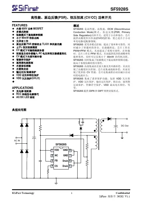
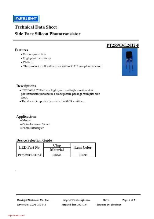
Technical Data Sheet Side Face Silicon PhototransistorPT2559B/L2/H2-FFeatures․Fast response time ․High photo sensitivity ․Pb free ․This product itself will remain within RoHS compliant version.Descriptions• PT2559B/L2/H2-F is a high speed and high sensitive dual phototransistor molded in a black plastic package with plat side view. • The device is spectrally matched with IR emitters.Applications• Mouse • Optoelectronic Switch • Photo InterrupterDevice Selection Guide LED Part No.PT2559B/L2/H2-FChip MaterialSiliconLens ColorBlack..Everlight Electronics Co., Ltd. Device No: CDPT-255-013http:\\ Prepared date: 2007/1/6Rev 1 Prepared by: zhouhongPage: 1 of 8/PT2559B/L2/H2-FPackage DimensionsNotes: 1.All dimensions are in millimeters 2.Tolerances unless dimensions ±0.25mmAbsolute Maximum Ratings (Ta=25℃)Parameter Collector-Emitter Voltage Emitter-Collector-Voltage Collector Current Operating Temperature Storage Temperature Lead Soldering Temperature(*1) Power Dissipation at (or below) 25℃ Free Air Temperature Symbol VCEO VECO IC Topr Tstg Tsol PD Rating 30 5 20 -25 ~ +85℃ -40 ~ +85℃ 260 75 Units V V mA ℃ ℃ ℃ mWNotes: *1:Soldering time≦5 seconds.Everlight Electronics Co., Ltd. Device No: CDPT-255-013http:\\ Prepared date: 2007/1/6Rev 1 Prepared by: zhouhongPage: 2 of 8/PT2559B/L2/H2-FElectro-Optical Characteristics (Ta=25℃)Parameter Collector – Emitter Breakdown Voltage Emitter-Collector Breakdown Voltage Collector-Emitter Saturation Voltage Rise Time Fall Time Collector Dark Current Symbol BVCEO BVECO VCE(sat) tr tf Condition IC=100μA Ee=0mW/cm2 IE=100μA Ee=0mW/cm2 IC=2mA Ee=1mW/cm2 Min 30 5 --Typ ------Max Unit ----0.4 --μS ----15 ----100 nA V V VVCE=5V IC=1mA RL =1000Ω Ee=0mW/cm2 VCE=20V VCE=5V, Ee=0.555mW/cm2 --------15ICEOOn State Collector Current Wavelength of Peak Sensitivity Rang of Spectral BandwidthIC(on) λp λ0.5129---1085 μA--760940 -----1100nm nmEverlight Electronics Co., Ltd. Device No: CDPT-255-013http:\\ Prepared date: 2007/1/6Rev 1 Prepared by: zhouhongPage: 3 of 8/PT2559B/L2/H2-FTypical Electro-Optical Characteristics CurvesFig.1 Power Dissipation vs. Ambient Temperature Fig.2 Spectral Sensitivity100 80 60 40 20 01.0 Ta=25 C 0.8 0.6 0.4 0.2-250255075 85 10001100 1200Fig.3 Dark Current vs. Ambient TemperatureFig. 4 Reverse Light Current vs. Ee10100 C10 1010 1 0.1 0.01 0.510 10 0 25 50 75 1001325Everlight Electronics Co., Ltd. Device No: CDPT-255-013http:\\ Prepared date: 2007/1/6Rev 1 Prepared by: zhouhongPage: 4 of 8/PT2559B/L2/H2-FTypical Electro-Optical Characteristics CurvesFig.5 Terminal Capacitance vs. Reverse Voltage`Fig.6 Response Time vs. Load Resistance160 140 120 100 80 60 40 20 0 0 10 20 30 40 50 60 70214 12 10 8 6 4 2 0 0 1 2 3 4Everlight Electronics Co., Ltd. Device No: CDPT-255-013http:\\ Prepared date: 2007/1/6Rev 1 Prepared by: zhouhongPage: 5 of 8/PT2559B/L2/H2-FReliability Test Item And ConditionThe reliability of products shall be satisfied with items listed below. Confidence level:90% LTPD:10% NO. Item 1 Solder Heat 2 Temperature Cycle L : -40℃ H :+100℃ 3 Thermal Shock L :-10℃ 4 5 High Temperature Storage Low Temperature Storage Test Conditions TEMP.:260℃ H : +100℃ 15mins 5mins 300Cycles 15mins 5mins 10secs 300Cycles 5mins 1000hrs 1000hrs 1000hrs 1000hrs 22pcs IC(ON)≦L×0.8 L:the initial test value 0/1 22pcs 0/1 Test Hours/ Sample Cycles Sizes 10secs 22pcs Failure Judgement Criteria Ac/Re 0/1TEMP.:+100℃ TEMP.:-40℃22pcs 22pcs 22pcs 22pcs0/1 0/1 0/1 0/16 DC Operating Life VCE=5V 7 High Temperature/ 85℃ / 85% R.H High HumidityEverlight Electronics Co., Ltd. Device No: CDPT-255-013http:\\ Prepared date: 2007/1/6Rev 1 Prepared by: zhouhongPage: 6 of 8/PT2559B/L2/H2-F█ Test Method For On State Collector Current :Condition : Ee=0.555mW/cm2 , VCE=5V Test Item : Collector Current [IC(on)] Unit : µA█ To Distinguish Intensity:Condition:VCE:5V A RanksColor CodeEe:0.555mW/cm2Symbol Min Typ Max Unit Test ConditionEe=0.555mW/c ㎡ VCE=5V Ee=0.555mW/c ㎡ VCE=5V Ee=0.555mW/c ㎡ VCE=5V Ee=0.555mW/c ㎡ VCE=5V Ee=0.555mW/c ㎡ VCE=5V Ee=0.555mW/c ㎡ VCE=5V Ee=0.555mW/c ㎡ VCE=5V Ee=0.555mW/c ㎡ VCE=5V Ee=0.555mW/c ㎡ VCE=5V Ee=0.555mW/c ㎡ VCE=5V Ee=0.555mW/c ㎡ VCE=5V Ee=0.555mW/c ㎡ VCE=5VRanksRed Blue Yellow Silver Green Purple White Brown Orange Golden Pink Red,BlueA1 A2 A3 A4 A5 A6 A7 A8 A9 A10 A11 A12IC(ON) IC(ON) IC(ON) IC(ON) IC(ON) IC(ON IC(ON IC(ON IC(ON IC(ON IC(ON) IC(ON)129 195 262 330 398 468 536 604 673 742 812 882-------------------------226 306 380 461 544 625 703 785 862 944 1018 1085μA μA μA μA μA μA μA μA μA μA μA μAEverlight Electronics Co., Ltd. Device No: CDPT-255-013http:\\ Prepared date: 2007/1/6Rev 1 Prepared by: zhouhongPage: 7 of 8/PT2559B/L2/H2-FPacking Quantity Specification1. 1000Pcs/1Bag,8Bags/1Box 2. 10Boxes/1CartonLabel Form SpecificationCPN: Customer’s Production Number P/N : Production Number QTY: Packing Quantity CAT: Ranks HUE: Peak Wavelength REF: Reference LOT No: Lot NumberPT2559B/L2/H2-FNotes1. Above specification may be changed without notice. EVERLIGHT will reserve authority on material change for above specification. 2. When using this product, please observe the absolute maximum ratings and the instructions for using outlined in these specification sheets. EVERLIGHT assumes no responsibility for any damage resulting from use of the product which does not comply with the absolute maximum ratings and the instructions included in these specification sheets. 3. These specification sheets include materials protected under copyright of EVERLIGHT corporation. Please don’t reproduce or cause anyone to reproduce them without EVERLIGHT’s consent.EVERLIGHT ELECTRONICS CO., LTD. Office: No 25, Lane 76, Sec 3, Chung Yang Rd, Tucheng, Taipei 236, Taiwan, R.O.CTel: 886-2-2267-2000, 2267-9936 Fax: 886-2267-6244, 2267-6189, 2267-6306 http:\\Everlight Electronics Co., Ltd. Device No: CDPT-255-013http:\\ Prepared date: 2007/1/6Rev 1 Prepared by: zhouhongPage: 8 of 8/分销商库存信息:EVERLIGHT PT2559B/L2-F PT2559B/L2/H2-F。