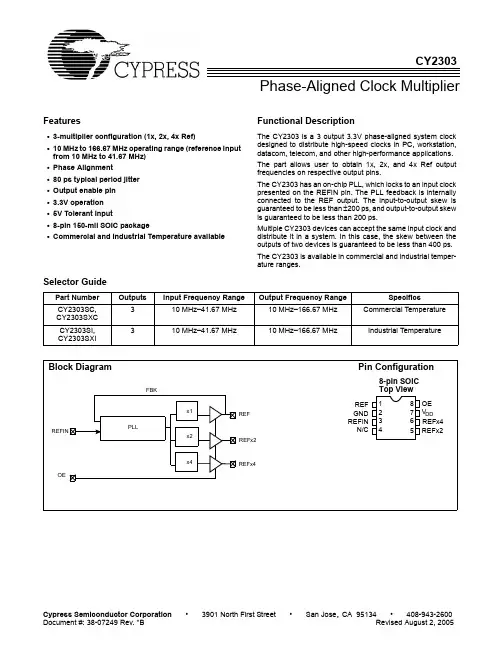
SI2303CDS中文资料
- 格式:pdf
- 大小:134.31 KB
- 文档页数:7
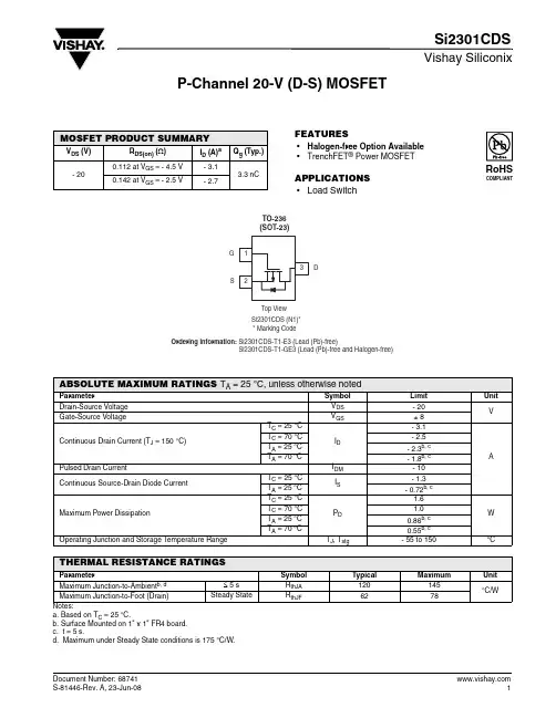
Vishay SiliconixSi2303CDSP-Channel 30-V (D-S) MOSFETFEATURES•TrenchFET ® Power MOSFET •100 % R g Tested •100 % UIS TestedAPPLICATIONS•Load SwitchMOSFET PRODUCT SUMMARYV DS (V)R DS(on) (Ω)I D (A)aQ g (Typ.)- 300.190 at V GS = - 10 V - 2.7 2 nC0.330 at V GS = - 4.5 V- 2.1Notes:a. Based on T C = 25 °C.b. Surface Mounted on 1" x 1" FR4 board.c. t = 5 s.d. Maximum under Steady State conditions is 160 °C/W.ABSOLUTE MAXIMUM RATINGS T A = 25°C, unless otherwise notedParameter Symbol Limit UnitDrain-Source Voltage V DS - 30VGate-Source Voltage V GS± 20Continuous Drain Current (T J = 150 °C)T C = 25 °C I D- 2.7AT C = 70 °C - 2.2T A = 25 °C - 1.9b, c T A = 70 °C - 1.5b, cPulsed Drain Current I DM - 10Continuous Source-Drain Diode CurrentT C = 25 °C I S - 1.75T A = 25 °C - 0.83b, cAvalanche Current L = 0.1 mHI AS - 5Single Pulse Avalanche Energy E AS 1.25mJ Maximum Power Dissipation T C = 25 °C P D 2.3WT C = 70 °C 1.5T A = 25 °C 1.0b, c T A = 70 °C 0.7b, cOperating Junction and Storage T emperature Range T J , T stg - 55 to 150°C THERMAL RESISTANCE RATINGSParameter Symbol Typical Maximum UnitMaximum Junction-to-Ambient b, d ≤ 5 s R thJA 80120°C/WMaximum Junction-to-Foot (Drain)Steady State R thJF 3555Vishay SiliconixSi2303CDSNotes:a. Pulse test; pulse width ≤ 300 µs, duty cycle ≤ 2 %.b. Guaranteed by design, not subject to production testing.Stresses beyond those listed under “Absolute Maximum Ratings” may cause permanent damage to the device. These are stress ratings only, and functional operation of the device at these or any other conditions beyond those indicated in the operational sections of the specifications is not implied. Exposure to absolute maximum rating conditions for extended periods may affect device reliability.MOSFET SPECIFICATIONS T J = 25°C, unless otherwise notedParameter Symbol Test Conditions Min.Typ.Max.U nit StaticDrain-Source Breakdown Voltage V DS V DS = 0 V , I D = - 250 µA- 30VV DS Temperature Coefficient ΔV DS /T J I D = - 250 µA - 27mV/°C V GS(th) T emperature Coefficient ΔV GS(th)/T J 3.8Gate-Source Threshold Voltage V GS(th) V DS = V GS , I D = - 250 µA - 1- 3V Gate-Source LeakageI GSS V DS = 0 V, V GS = ± 20 V ± 100nA Zero Gate Voltage Drain Current I DSS V DS = - 30 V , V GS = 0 V - 1µA V DS = - 30 V , V GS = 0 V , T J = 55 °C- 10On-State Drain Current aI D(on) V DS ≤ - 5 V, V GS = - 10 V - 10A Drain-Source On-State Resistance aR DS(on) V GS = - 10 V , I D = - 1.9 A 0.1580.190ΩV GS = - 4.5 V , I D = - 1.4 A 0.2750.330Forward T ransconductance a g fsV DS = - 5 V, I D = - 1.9 A2SDynamic bInput Capacitance C iss V DS = - 15 V , V GS = 0 V, f = 1 MHz155pFOutput CapacitanceC oss 35Reverse Transfer Capacitance C rss 25Total Gate Charge Q g V DS = - 15 V , V GS = - 10 V , ID = - 1.9 A 48nC V DS = - 15 V , V GS = - 4.5 V , I D = - 1.9 A 24Gate-Source Charge Q gs 0.6Gate-Drain Charge Q gd 1Gate Resistance R g f = 1 MHz1.78.517ΩTurn-On Delay Time t d(on) V DD = - 15 V , R L = 10 ΩI D = - 1.5 A, V GEN = - 10 V, R G = 1 Ω48nsRise Timet r 1118Turn-Off Delay Time t d(off) 1118Fall Timet f 816Turn-On Delay Time t d(on) V DD = - 15 V , R L = 10 ΩI D ≅ - 1.5 A, V GEN = - 4.5 V , R G = 1 Ω3644Rise Timet r 3745Turn-Off Delay Time t d(off) 1218Fall Timet f914Drain-Source Body Diode Characteristics Continuous Source-Drain Diode Current I S T C = 25 °C- 1.75A Pulse Diode Forward Current a I SM - 10Body Diode VoltageV SD I S = - 1.5 A- 0.8- 1.2V Body Diode Reverse Recovery Time t rr I F = - 1.5 A, di/dt = 100 A/µs, T J = 25 °C1726ns Body Diode Reverse Recovery Charge Q rr 914nC Reverse Recovery Fall Time t a 12nsReverse Recovery Rise Timet b5On-Resistance vs. Drain Current and Gate VoltageCapacitanceOn-Resistance vs. Junction TemperatureThreshold VoltageSafe Operating AreaVishay SiliconixSi2303CDSTYPICAL CHARACTERISTICS 25°C, unless otherwise noted* The power dissipation P D is based on T J(max) = 150 °C, using junction-to-case thermal resistance, and is more useful in settling the upper dissipation limit for cases where additional heatsinking is used. It is used to determine the current rating, when this rating falls below the package limit.Vishay SiliconixSi2303CDSTYPICAL CHARACTERISTICS 25°C, unless otherwise notedVishay Siliconix maintains worldwide manufacturing capability. Products may be manufactured at one of several qualified locations. Reliability data for Silicon Technology and Package Reliability represent a composite of all qualified locations. For related documents such as package/tape drawings, part marking, and reliability data, see /ppg?69991.Normalized Thermal Transient Impedance, Junction-to-FootDisclaimer Legal Disclaimer NoticeVishayAll product specifications and data are subject to change without notice.Vishay Intertechnology, Inc., its affiliates, agents, and employees, and all persons acting on its or their behalf (collectively, “Vishay”), disclaim any and all liability for any errors, inaccuracies or incompleteness contained herein or in any other disclosure relating to any product.Vishay disclaims any and all liability arising out of the use or application of any product described herein or of any information provided herein to the maximum extent permitted by law. The product specifications do not expand or otherwise modify Vishay’s terms and conditions of purchase, including but not limited to the warranty expressed therein, which apply to these products.No license, express or implied, by estoppel or otherwise, to any intellectual property rights is granted by this document or by any conduct of Vishay.The products shown herein are not designed for use in medical, life-saving, or life-sustaining applications unless otherwise expressly indicated. Customers using or selling Vishay products not expressly indicated for use in such applications do so entirely at their own risk and agree to fully indemnify Vishay for any damages arising or resulting from such use or sale. Please contact authorized Vishay personnel to obtain written terms and conditions regarding products designed for such applications.Product names and markings noted herein may be trademarks of their respective owners.元器件交易网。