基于FPGA的数字存储示波器的设计毕业设计
- 格式:doc
- 大小:6.42 MB
- 文档页数:74
基于FPGA和单片机的数字存储示波器摘要:随着时代的发展,示波器作为电子行业中一种常用的测试工具,在电子技术工作中起着不可替代的作用。
目前新的技术应用越来越多,用户的测试需求不断变化,然而市面上的数字存储示波器大多价格昂贵、体型庞大,很难携带或者安放,对于一些只进行简单测量不太实用。
数字存储示波器是20世纪70年代,发展起来的一种新型示波器。
今后市场的发展让示波器需要面对更多的应用,数字示波器功能集成趋势明显,与此同时,除了追求强大的功能以外,外观精美、款式小巧,便于携带也成为一个发展趋势。
本次设计利用单片机、FPGA和AD设计一款大众化的数字滤波器,成本低、体积小、便于携带、使用方便,能够完成基本的测试,如:存储并显示波形,测量信号的频率、幅度等。
1 方案论证与比较1.1 方案一:DSP+FPGA开发起来比较灵活,升级也较为容易,通用性较强。
同时利用了DSP运算速度来提高整个系统的算法效率;同时采用这种架构开发起来相对比较简单,因为它结合了FPGA 和DSP两者的优点。
所以它适合于实时信号处理。
在实时信号处理的过程中,对DSP的速度要求高,这样能同时使得整个系统既有其高速的处理速度,同时也不失其灵活性。
但是DSP在和与外围电路接口的时候,比如说LCD显示器和键盘电路进行通信的时候,因为DSP速度非常快。
而LCD和键盘的速度都很慢,DSP的优势没有得到利用。
1.2 方案二:利用超大规模可编程器件FPGA来控制高速A/D转换器和RAM实现高速数据采集,并且用它来进行数据的存储与处理。
由于超大规模可编程器件是全硬件的,所以速度快,稳定性好,利用较少的外围器件就可以实现复杂的逻辑和时序控制功能,是较为理想的方案。
这种方案实际上是一种片上系统(System On Chip),即用单个芯片完成所有的控制与数据处理,并且还是全硬件的。
但是该方案实现起来非常困难,并且成本非常高,所以没有采用这种方案。
1.3 方案三:该方案采用FPGA和MSP430单片机来实现。
【FPGA设计实例】基于FPGA的数字示波器设计Digital oscilloscopeA digital oscilloscope has many advantages over its analog counterpart, like the ability to capture single events, and to display what happens before the trigger.You can build a digital oscilloscope simply by hooking an ADC and an FPGA together.This particular design uses an 100MHz flash ADC, so we are building an 100MSPS(mega-samples-per-seconds) oscilloscope.This oscilloscope design is interesting because it shows how powerful and useful modern FPGAs can be. But if you are new to FPGA technology, keep that in mind this is not the easiest design to understand on this site.HDL designOr how to create the oscilloscope logic inside the FPGA.•HDL part 1 - FIFO-based design.•HDL part 2 - RAM-based design.•HDL part 3 - Trigger mechanism.•HDL part 4 - More functionality.Hardware•This design was created using the Flashy boards.•See also the "hands-on" page on how to build a simple oscilloscope. Software•History, features, screen shots.•See also the interference patterns page.ScreenshotHere's the view of a 27MHz signal, sampled at 100MHz and reconstructed using the "sample equivalent time" technique.Digital oscilloscope - part 1Here's what is built here:The FPGA receives 2 clocks:• A slow "system" clock, fixed at 25MHz.•An ADC sampling clock (something faster, let's say 100MHz), that is connected to both the ADC and the FPGA.Having these 2 clocks gives flexibility to the design. But that also means we need a way to transfer information from one clock domain to the other. To validate that the hardware works,let's go the easy route and use a FIFO. The acquired samples from the ADC are stored in the FPGA FIFO at full ADC speed (100MHz).Then, the FIFO content is read back, serialized and sent on a serial port at a much slower speed (115200 baud). Finally we connect the serial output to a PC that receives each byte and displays a signal trace.For this first attempt, there is no trace triggering mechanism. The ADC storage starts at random intervals so the trace will jump left and right, but that's fine for now.Design considerationsAt 100MHz, the FIFO fills up in about 10us. That's pretty fast. Once full, we have to stop feeding it. What is stored needs to be completely sent to the PC before we can start feeding the FIFO again.The serial communication used here works at 115200 bauds, so roughly 10KBytes/s. 1024 samples take about 100ms to transmit. During that time, the oscilloscope is "blind", because we discard the data coming from the ADC. So it is blind 99.99% of the time. That's typical of this type of architecture.That can be partially compensated when we add a trigger mechanism later, because while the trigger is armed, it works at full ADC speed and can stay armed as long as it takes for the trigger condition to happen. More on that later.Register the inputsThe ADC output data bus is connected to the FPGA using 8 pins that we call "data_flash[7:0]". These come at speed of up to 100MHz. Since this is fast, it is best to "register" them right when they come in the FPGA.reg [7:0] data_flash_reg;always @(posedge clk_flash) data_flash_reg <= data_flash;Now "data_flash_reg" is fully internal to the FPGA and can be fed to the FPGA FIFO. The FIFOThe FIFO is 1024 words deep x 8 bits wide. Since we receive 8 bits per clock from the ADC, we can store 1024 ADC samples. At 100MHz, it takes about 10us to fill up the FIFO.The FIFO uses synchronous static RAM blocks available inside the FPGA. Each storage block can store typically 512x8bits. So the FIFO uses 2 blocks.The FIFO logic itself is created by using the FPGA vendor "function builder". Xilinx calls it "coregen" while Altera "Megafunctions wizard". Here let's use Altera's Quartus to create this file.So now, using the FIFO is just a connectivity issue.fifomyfifo(.data(data_flash_reg), .wrreq(wrreq), .wrclk(clk_flash), .wrfull(wrfull), .wrempty(w rempty), .q(q_fifo), .rdreq(rdreq), .rdclk(clk), .rdempty(rdempty));Using a FIFO is nice because it takes care of the different clocks. We connected the write side of the FIFO to the "clk_flash" (100MHz), and the read side of the FIFO to "clk" (25MHz).The FIFO provides the full and empty signals for each clock domain. For example, "wrempty" is an empty signal that can be used in the write clock domain ("clk_flash"), and "rdempty" can be used in the read clock domain ("clk").Using the FIFO is simple: Writing to it is just a matter of asserting the "wrreq" signal (and providing the data to the ".data" port), while reading from it a matter of asserting "rdreq" (and the data comes on the ".q" port).Writing to the FIFOTo start writing to the FIFO, we wait until it is empty. Of course, at power-up (after the FPGA is configured), that is true.We stop only when it gets full. And then the process starts again... we wait until it is empty... feed it until it is full... stop.reg fillfifo;always @(posedge clk_flash)if(~fillfifo)fillfifo <= wrempty; // start when emptyelsefillfifo <= ~wrfull; // stop when fullassign wrreq = fillfifo;Reading to the FIFOWe read from the FIFO as long as it is not empty. Each byte read is send to a serial output.wire TxD_start = ~TxD_busy & ~rdempty;assign rdreq = TxD_start;async_transmitterasync_txd(.clk(clk), .TxD(TxD), .TxD_start(TxD_start), .TxD_busy(TxD_busy), .TxD_data( q_fifo));We use the async_transmitter module to serialize the data and transmit it to a pin called "TxD".Complete designOur first working oscilloscope design, isn't that nice?module oscillo(clk, TxD, clk_flash, data_flash);input clk;output TxD;input clk_flash;input [7:0] data_flash;reg [7:0] data_flash_reg; always @(posedge clk_flash) data_flash_reg <= data_flash;wire [7:0] q_fifo;fifomyfifo(.data(data_flash_reg), .wrreq(wrreq), .wrclk(clk_flash), .wrfull(wrfull), .wrempty(w rempty), .q(q_fifo), .rdreq(rdreq), .rdclk(clk), .rdempty(rdempty));// The flash ADC side starts filling the fifo only when it is completely empty,// and stops when it is full, and then waits until it is completely empty againreg fillfifo;always @(posedge clk_flash)if(~fillfifo)fillfifo <= wrempty; // start when emptyelsefillfifo <= ~wrfull; // stop when fullassign wrreq = fillfifo;// the manager side sends when the fifo is not emptywire TxD_busy;wire TxD_start = ~TxD_busy & ~rdempty;assign rdreq = TxD_start;async_transmitterasync_txd(.clk(clk), .TxD(TxD), .TxD_start(TxD_start), .TxD_busy(TxD_busy), .TxD_data( q_fifo));endmoduleDigital oscilloscope - part 2The FIFO allowed us to get a working design very quickly.But for our simple oscilloscope, it is overkill.We need a mechanism to store data from one clock domain (100MHz) and read it in another (25MHz). A simple dual-port RAM does that.The disadvantage of not using a FIFO is that all the synchonization between the 2 clock domains (that the FIFO was doing for us) has to be done "manually" now.TriggerThe "FIFO based" oscilloscope design didn't have an explicit trigger mechanism.Let's change that. Now the oscilloscope will be triggered everytime it receives a character from the serial port. Of course, that's still not a very useful design, but we'll improved on that later.We receive data from the serial port:wire [7:0] RxD_data;async_receiverasync_rxd(.clk(clk), .RxD(RxD), .RxD_data_ready(RxD_data_ready), .RxD_data(RxD_data ));Everytime a new character is received, "RxD_data_ready" goes high for one clock. We use that to trigger the oscilloscope.SynchronizationWe need to transfer this "RxD_data_ready went high" information from the "clk" (25MHz) domain to the "clk_flash" (100MHz) domain.First, a signal "startAcquisition" goes high when a character is received.reg startAcquisition;wire AcquisitionStarted;always @(posedge clk)if(~startAcquisition)startAcquisition <= RxD_data_ready;elseif(AcquisitionStarted)startAcquisition <= 0;We use synchronizers in the form of 2 flipflops (to transfer this "startAcquisition" to the other clock domain).reg startAcquisition1; always @(posedge clk_flash) startAcquisition1 <= startAcquisition; reg startAcquisition2; always @(posedge clk_flash) startAcquisition2 <= startAcquisition1;Finally, once the other clock domain "sees" the signal, it "replies" (using another synchronizer "Acquiring").reg Acquiring;always @(posedge clk_flash)if(~Acquiring)Acquiring <= startAcquisition2; // start acquiring?elseif(&wraddress) // done acquiring?Acquiring <= 0;reg Acquiring1; always @(posedge clk) Acquiring1 <= Acquiring;reg Acquiring2; always @(posedge clk) Acquiring2 <= Acquiring1;assign AcquisitionStarted = Acquiring2;The reply resets the original signal.Dual-port RAMNow that the trigger is available, we need a dual-port RAM to store the data.Notice how each side of the RAM uses a different clock.ram512 ram_flash(.data(data_flash_reg), .wraddress(wraddress), .wren(Acquiring), .wrclock(clk_flash),.q(ram_output), .rdaddress(rdaddress), .rden(rden), .rdclock(clk));The ram address buses are created easily using binary counters.First the write address:reg [8:0] wraddress;always @(posedge clk_flash) if(Acquiring) wraddress <= wraddress + 1;and the read address:reg [8:0] rdaddress;reg Sending;wire TxD_busy;always @(posedge clk)if(~Sending)Sending <= AcquisitionStarted;elseif(~TxD_busy)beginrdaddress <= rdaddress + 1;if(&rdaddress) Sending <= 0;endNotice how each counter uses a different clock.Finally we send data to the PC:wire TxD_start = ~TxD_busy & Sending;wire rden = TxD_start;wire [7:0] ram_output;async_transmitterasync_txd(.clk(clk), .TxD(TxD), .TxD_start(TxD_start), .TxD_busy(TxD_busy), .TxD_data( ram_output));The complete designmodule oscillo(clk, RxD, TxD, clk_flash, data_flash);input clk;input RxD;output TxD;input clk_flash;input [7:0] data_flash;///////////////////////////////////////////////////////////////////wire [7:0] RxD_data;async_receiverasync_rxd(.clk(clk), .RxD(RxD), .RxD_data_ready(RxD_data_ready), .RxD_data(RxD_data ));reg startAcquisition;wire AcquisitionStarted;always @(posedge clk)if(~startAcquisition)startAcquisition <= RxD_data_ready;elseif(AcquisitionStarted)startAcquisition <= 0;reg startAcquisition1; always @(posedge clk_flash) startAcquisition1 <= startAcquisition ; reg startAcquisition2; always @(posedge clk_flash) startAcquisition2 <= startAcquisition1;reg Acquiring;always @(posedge clk_flash)if(~Acquiring)Acquiring <= startAcquisition2;elseif(&wraddress)Acquiring <= 0;reg [8:0] wraddress;always @(posedge clk_flash) if(Acquiring) wraddress <= wraddress + 1;reg Acquiring1; always @(posedge clk) Acquiring1 <= Acquiring;reg Acquiring2; always @(posedge clk) Acquiring2 <= Acquiring1;assign AcquisitionStarted = Acquiring2;reg [8:0] rdaddress;reg Sending;wire TxD_busy;always @(posedge clk)if(~Sending)Sending <= AcquisitionStarted;elseif(~TxD_busy)beginrdaddress <= rdaddress + 1;if(&rdaddress) Sending <= 0;endwire TxD_start = ~TxD_busy & Sending;wire rden = TxD_start;wire [7:0] ram_output;async_transmitterasync_txd(.clk(clk), .TxD(TxD), .TxD_start(TxD_start), .TxD_busy(TxD_busy), .TxD_data( ram_output));///////////////////////////////////////////////////////////////////reg [7:0] data_flash_reg; always @(posedge clk_flash) data_flash_reg <= data_flash;ram512 ram_flash(.data(data_flash_reg), .wraddress(wraddress), .wren(Acquiring), .wrclock(clk_flash),.q(ram_output), .rdaddress(rdaddress), .rden(rden), .rdclock(clk));endmoduleDigital oscilloscope - part 3Our first trigger is simple - we detect a rising edge crossing a fixed threshold. Since we use an 8-bit ADC, the acquisition range goes from 0x00 to 0xFF.So let's set the threshold to 0x80 for now.Detecting a rising edgeIf a sample is above the threshold, but the previous sample was below, trigger!reg Threshold1, Threshold2;always @(posedge clk_flash) Threshold1 <= (data_flash_reg>=8'h80);always @(posedge clk_flash) Threshold2 <= Threshold1;assign Trigger = Threshold1 & ~Threshold2; // if positive edge, trigger!Mid-display triggerOne great feature about a digital scope is the ability to see what's going on before the trigger.How does that work?The oscilloscope is continuously acquiring. The oscilloscope memory gets overwritten over and over - when we reach the end, we start over at the beginning. But if a trigger happens, the oscilloscope keeps acquiring for half more of its memory depth, and then stops. So it keeps half of its memory with what happened before the trigger, and half of what happened after.We are using here a 50% or "mid-display trigger" (other popular settings would have been 25% and 75% settings, but that's easy to add later).The implementation is easy. First we have to keep track of how many bytes have been stored. reg [8:0] samplecount;With a memory depth of 512 bytes, we first make sure to acquire at least 256 bytes, then stop counting but keep acquiring while waiting for a trigger. Once the trigger comes, we start counting again to acquire 256 more bytes, and stop.reg PreTriggerPointReached;always @(posedge clk_flash) PreTriggerPointReached <= (samplecount==256);The decision logic deals with all these steps:always @(posedge clk_flash)if(~Acquiring)beginAcquiring <= startAcquisition2; // start acquiring?PreOrPostAcquiring <= startAcquisition2;endelseif(&samplecount) // got 511 bytes? stop acquiringbeginAcquiring <= 0;AcquiringAndTriggered <= 0;PreOrPostAcquiring <= 0;endelseif(PreTriggerPointReached) // 256 bytes acquired already?beginPreOrPostAcquiring <= 0;endelseif(~PreOrPostAcquiring)beginAcquiringAndTriggered <= Trigger; // Trigger? 256 more bytes and we're set PreOrPostAcquiring <= Trigger;if(Trigger) wraddress_triggerpoint <= wraddress; // keep track of where the trigger happenedendalways @(posedge clk_flash) if(Acquiring) wraddress <= wraddress + 1;always @(posedge clk_flash) if(PreOrPostAcquiring) samplecount <= samplecount + 1;reg Acquiring1; always @(posedge clk) Acquiring1 <= AcquiringAndTriggered;reg Acquiring2; always @(posedge clk) Acquiring2 <= Acquiring1;assign AcquisitionStarted = Acquiring2;Notice that we took care of remembering where the trigger happened. That's used to determine the beginning of the sample window in the RAM to send to the PC.reg [8:0] rdaddress, SendCount;reg Sending;wire TxD_busy;always @(posedge clk)if(~Sending)beginSending <= AcquisitionStarted;if(AcquisitionStarted) rdaddress <= (wraddress_triggerpoint ^ 9'h100);endelseif(~TxD_busy)beginrdaddress <= rdaddress + 1;SendCount <= SendCount + 1;if(&SendCount) Sending <= 0;endDigital oscilloscope - part 4Now that the oscilloscope skeleton is working, it is easy to add more functionality. Edge-slope triggerLet's add the ability to trigger on a rising-edge or falling-edge. Any oscilloscope can do that.We need one bit of information to decide with direction we want to trigger on. Let's use bit-0 of the data sent by the PC.assign Trigger = (RxD_data[0] ^ Threshold1) & (RxD_data[0] ^ ~Threshold2);That was easy.More optionsLet's add the ability to control the trigger threshold. That's an 8-bits value. Then we require horizontal acquisition rate control, filtering control... That requires multiple control bytes from the PC to control the oscilloscope.The simplest approach is to use the "async_receiver" gap detection feature. The PC sends control bytes in burst, and when it stops sending, the FPGA detects it and assert an "RxD_gap" signal.wire RxD_gap;async_receiverasync_rxd(.clk(clk), .RxD(RxD), .RxD_data_ready(RxD_data_ready), .RxD_data(RxD_data ), .RxD_gap(RxD_gap));reg [1:0] RxD_addr_reg;always @(posedge clk) if(RxD_gap) RxD_addr_reg <= 0; else if(RxD_data_ready)RxD_addr_reg <= RxD_addr_reg + 1;// register 0: TriggerThresholdreg [7:0] TriggerThreshold;always @(posedge clk) if(RxD_data_ready & (RxD_addr_reg==0)) TriggerThreshold <=RxD_data;// register 1: "0 0 0 0 HDiv[3] HDiv[2] HDiv[1] HDiv[0]"reg [3:0] HDiv;always @(posedge clk) if(RxD_data_ready & (RxD_addr_reg==1)) HDiv <=RxD_data[3:0];// register 2: "StartAcq TriggerPolarity 0 0 0 0 0 0"reg TriggerPolarity;always @(posedge clk) if(RxD_data_ready & (RxD_addr_reg==2)) TriggerPolarity <= RxD_data[6];wire StartAcq = RxD_data_ready & (RxD_addr_reg==2) & RxD_data[7];We've also added a 4 bits register (HDiv[3:0]) to control the horizontal acquisition rate. When we want to decrease the acquisition rate, either we discard samples coming from the ADC, or we filter/downsample them at the frequency we are interested in.More and more featuresAs you can see, there are lots of features that can be added. The interesting thing is that you can design the oscilloscope the way you need it - maybe a special trigger mechanism? a special filtering function?Your turn to experiment.。
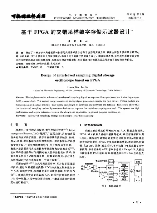
摘要高速数字化采样技术和FPGA技术的发展,已经开始对传统测试仪器,包括现有的数字化仪器发展产生着深刻的影响,对传统仪器体系结构,传统测量方法,传统仪器的定义和分类等都将产生深刻的变革。
近几年来,数字仪器通常采用DSP或FPGA结构,从信息处理技术的发展上看,以FPGA为基础的软件硬件化是其重要的发展方向,本文设计的基于FPGA的数字示波器,是由单片机和FPGA相结合的方式组成,即用单片机完成人机界面,系统调控,用FPGA完成数据采集,数据处理等功能。
由通道输入调整,数据采集,数据处理,波形显示和操作界面等功能模块组成,系统中的数据采集及数据处理模块,采用了FPGA 内制的RAM IP核,使系统的工作频率基本不受外围器件影响。
设计中采用了自顶向下的方法,将系统按逻辑功能划分模块,各模块使用VHDL语言进行设计,在ISE中完成软件的设计和仿真关键词:FPGA 数字示波器数字采样AbstractHigh-speed digital sampling and FPGA technology has begun to influnence the development of traditional test equipment, including existing digital instruments , the architecture of traditional instruments, traditional measurement methods, definition and classification of traditional instruments and so will produce profound changes.In recent years, independent instrument is made up of DSP or FPGA structure, from the point of information processing technology development, to FPGA based hardware of software is an important direction of development, the paper design FPGA-based digital oscilloscope, which combines a single chip and FPGA , namely, with a microcontroller for interface and system control, with the FPGA for data acquisition, data processing and other functions. It is made up of adjustable channel input, data acquisition, data processing,waveform display and user interface features such as modules, the system of data collection and data processing module, using the FPGA within the system RAM IP core, which make a great significance on the data processing speed and real-time entry requirements. Using top-down approach, the system is logical and functional modules, each module is designed using the VHDL language, completed in the ISE software .Keywords: FPGA,Digital Oscilloscope,Digital Sampling目录摘要 (1)第一章绪论 (5)1.1研究概况与意义 (5)1.2 主要工作 (6)第二章数字示波器的工作原理 (8)2.1 工作原理框图 (8)2.1.1 数字示波器系统框图 (8)2.2 采样定理 (9)2.3 频率测量 (10)2.3.1高频双计数器测量方法 (10)2.3.2大范围双计数器测量法 (11)2.3.3 等精度测量法 (11)2.4扫描速度 (12)第三章硬件电路 (13)3.1 系统组成结构 (13)3.2放大电路 (14)3.2.1程控衰减放大器电路 (15)3.2.2 ADS830的应用 (16)3.2.3 放大器AD603介绍 (17)3.3整形电路 (20)3.3.1信号整形电路设计 (20)3.4采样与保持电路 (21)3.4.1 随机采样 (21)3.4.2 采样与保持电路设计 (22)3.5 数据采集电路 (22)3.5.1 FIFO的选择 (23)3.5.2 随机采样展宽电路 (23)3.6 电路的保护及滤波处理 (24)第四章 FPGA软件设计及仿真 (25)4.1分频电路及产生A/D转换器的控制信号 (25)4.2 FIFO功能单元设计 (26)4.3双口RAM (27)4.4液晶显示及键盘模块 (27)4.5系统软件住程序设计 (28)第五章实验结果 (29)5. 1 垂直灵敏度测试 (29)5. 2 水平扫描速度的测试 (29)总结 (30)参考文献 (31)第一章绪论与传统模拟示波器相比,数字示波器不仅具有可存储波形、体积小、功耗低,使用方便等优点,而且还具有强大的信号实时处理分析功能。
基于FPGA的简易可存储示波器设计
摘要:本文介绍了一种基于FPGA 的采样速度60Mbit/s 的双通道简易数字示波器设计,能够实现量程和采样频率的自动调整、数据缓存、显示以及与计算机之间的数据传输。
关键词:数据采集;数字示波器;FPGA
引言
传统的示波器虽然功能齐全,但是体积大、重量重、成本高、等一系列问题使应用受到了限制。
有鉴于此,便携式数字存储采集器就应运而生,它采用了LCD 显示、高速A/D 采集与转换、ASIC 芯片等新技术,具有很强的实用性和巨大的市场潜力,也代表了当代电子测量仪器的一种发展趋势,即向功能多、体积小、重量轻、使用方便的掌上型仪器发展。
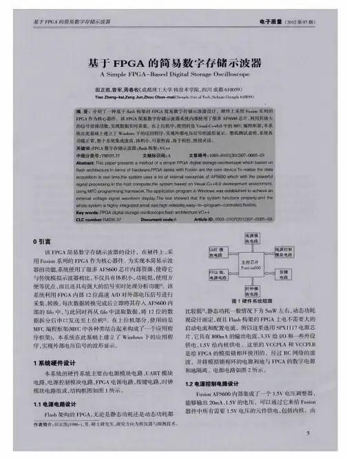
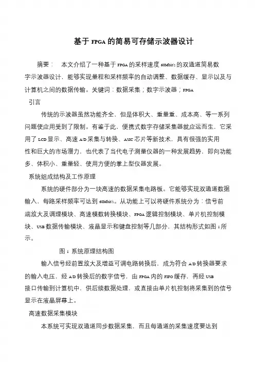
系统组成结构及工作原理
系统的硬件部分为一块高速的数据采集电路板。
它能够实现双通道数据输入,每路采样频率可达到60Mbit/s。
从功能上可以将硬件系统分为:信号前端放大及调理模块、高速模数转换模块、FPGA 逻辑控制模块、单片机控制模块、USB 数据传输模块、液晶显示和键盘控制等几部分,其结构形式如图1 所示。
图1 系统原理结构图
输入信号经前置放大及增益可调电路转换后,成为符合A/D 转换器要求的输入电压,经A/D 转换后的数字信号,由FPGA 内的FIFO 缓存,再经USB 接口传输到计算机中,供后续数据处理,或直接由单片机控制将采集到的信号显示在液晶屏幕上。
高速数据采集模块
本系统可实现双通道同步数据采集,而且每通道的采集速度要达到。

第九届电子设计竞赛论文所在院系:电控学院题目:基于FPGA嵌入式的双通道数字存储示波器作者:朱俊兰方威夏俊伟指导老师:柴钰二○一一年五月基于FPGA嵌入式的双通道数字存储示波器摘要:本设计是以FPGA为核心,结合衰减电路、程控放大电路、ADC采样、整形测频电路以及VGA显示模块实现了双通道数字存储示波器的设计。
用户可以获取当前输入波形的峰峰值、频率等信息,另外用户可以对波形实现存储和回显功能。
双通道的设计使得用户可以同时观察和对比两路波形,设计时充分利用了FPGA的高速数据处理能力,嵌入了诸多IP 软核组成SOPC系统,尤其是NiosII软核的嵌入,使得在一块FPGA上完成了数据采集、存储、处理、显示等所有功能,使得系统更为简洁、稳定。
关键词:FPGA NiosII SOPC VGA ADS830E1、引言数字存储示波器(Digital Storage Oscilloscopes,简称DSO)是随着数字模拟电路技术和数字处理技术(尤其是微型计算机的发展)的发展而日益强大的一种具有存储波形功能的示波器。
和传统示波器相比,数字示波器具有体积轻巧功耗低、使用方便且波形可存储,对波形可以进行复杂数学分析等优点。
在诸多领域中,数字示波器已经完全取代模拟示波器,但是在国内,数字示波器的市场一直为外国厂商(安捷伦、泰克等)虽占据,而且价格不菲,这样,对于像我们学生这样的消费者根本无法支付,那么,本文就基于此,研究探讨了一种基于FPGA的DIY示波器的方案。
经过我们的不断测试,在低端场合,这样一款数字示波器完全合乎需求。
2、方案设计2.1总体方案描述系统的组成框图如图2.1所示,包括输入信号耦合选择、双路程控衰减放大、数据采集存储、数据处理、数据显示等部分。
信号分别从通道1、通道2输入,送入程控放大(衰减)电路进行放大(衰减),再对被放大(衰减)的信号进行电平调整后,送入高速ADC 对信号进行采样,FPGA则用于完成系统高速采样信号的存储及分频,并将波形显示在显示模块上。
基于FPGA的数字存储示波器对外围芯片的控制设计
数字存储作为测试技术的重要工具,被广泛应用于各个领域,并逐步取代传统模拟示波器。
其采样数据是波形运算和分析的基础,挺直影响到囫囵数字存储示波器的精确性。
从这点出来,提出采纳现场可编程规律器件( ) 作为数字存储示波器采样控制系统的核心,从芯片间有效帮助的角度,基于FPGA 设计接口通信控制模块和外围芯片驱动功能模块,以FPGA 为核心有效地组织其它芯片,共同完成数字存储示波器数据采样过程,确保数据按需求采样,有效地提高数字存储示波器的采样效率和数据的牢靠性。
1 数字存储示波器的总体设计计划
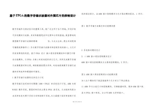
数字存储示波采纳双处理器( ARM + FPGA) 的系统设计计划,ARM 内嵌WINCE 操作系统,囫囵采样系统主要在FPGA 里完成,从功能的角度分成采样信息处理子系统与采样控制子系统,本文着重介绍采样控制子系统的驱动部分,由ARM 接口控制模块与芯片驱动模块组成。
1 所示: 图1 数字存储示波器总体功能模块图
2 系统驱动模块设计
2. 1 ARM 接口通信控制模块设计
ARM 接口通信控制模块为主要的控制模块,2 所示。
图2 ARM 接口通信控制部分功能模块图
加入这个模块而不挺直链接两个芯片有以下两点缘由:
1) ARM 作为主控芯片的控制模块,引脚数量有限。
假如ARM 接口挺直与FPGA 接口相连,会占用ARM 过多的接口。
第1页共8页。
设计摘要便携式数字存储示波器是现代示波器发展的方向之一,但由于其技术含量及高,尚无本国产品上市,属于测试仪表方面众目交注的领域。
ARM是32位的RISC 处理器,高性能、低功耗是其显著特点,已被广泛应用与各种潜入式领域。
在便携式电子产品的设计中,采用FPGA器件可以将原来的电路板级产品集成为芯片级产品,做到功耗低、可靠性高。
本文提出了一种基于ARM+FPGA结构的便携式数字存储示波器硬件平台设计方案,FPGA主要用于大量的数据存储,ARM则负责数据的进一步处理和控制波形的重建、显示和数据永久存储。
系统的前端芯片选用Altera公司最新一代的MAX Ⅱ系列高性能、低功耗FPGA芯片,系统后端ARM处理器则选用三星公司基于ARM7TDMI-S内核的多功能、低功耗ARM单片机——LPC2210,系统利用彩色LCD作为终端显示设设备,利用其基于自带的存储器存储永久波形数据,且自带有JTAG调试接口,便于设计。
ABSTRACTIt is one of the directions of modern oscilloscope development that the portable digital storage oscilloscope, because its technological content is extremely high, there are no national products to go on the market, It is a field concerned by a lot of eyes in testing the instrument. ARM is 32 bits RISC processor, high performance, low consumption are its remarkable characteristic, have already widely used in various kinds of embedded fields. In portable electronic product design, using FPGA may upgrade printed circuit product to integration circuit, depress power consumption and enhance reliability.The paper has proposed a kind of hardware platform design plan of the portable digital storage oscilloscope based on ARM+FPGA structure. FPGA is used as data memory, ARM is responsible for the back end waveform rebuilding, displaying and the data storing for ever. The chip of the systematic front, we select Altera Company’s MAX Ⅱseries for use that is the most new generation high performance, lowconsumption FPGA chip, the ARM processor of the systematic back end, we select Samsung Company’s the multi-functional、low consumption ARM chip based on ARM7TDMI-S kernel ——lpc2210, the system utilizes multicolor LCD as the terminal display device, to utilize the memory of lpc2210 to store the waveform data for ever, the JTAG debugging interface of lpc2210 make it convenient for design. Key words ARM Embedded Monitoring System, Portable Digital Storage Oscilloscope, Redundant date lost by hardware, LCD目录摘要 (I)ABSTRACT (I)1 绪论 (3)2 设计要求 (3)2.1 方案设计 (3)2.2 实现的功能和技术指标 (4)3 单片机LPC2210简介 (5)3.1 ARM处理器核简介 (5)3.1.1 ARM嵌入式系统 (5)3.1.2 ARM处理器介绍 (6)3.1.3程序状态寄存器 (6)3.2 单片32位微控制器-LPC2210 (7)3.2.1 LPC2210介绍 (7)3.2.2特性 (7)3.2.3结构框图 (7)3.2.4管脚信息 (8)3.2.5功能描述 (8)4 硬件平台的模块介绍 (10)4.1信号调理电路 (10)4.1.1 输入信号保护和衰减电路的设计 (10)4.1.2 信号放大电路的设计 (11)4.2 A/D转换模块 (12)4.2.1特性 (12)4.2.2描述 (12)4.2.3操作 (14)4.3 显示模块 (14)4.4键盘输入模块 (15)4.4.1 ZLG7290芯片描述 (15)4.4.2 I2C接口 (18)5软件开发环境介绍 (22)5.1 ADS 1.2 集成开发环境的组成 (23)5.2 CodeWarrior IDE 简介 (23)5.3 Easy JTAG防真器的安装与运用 (23)5.4 安装EasyJTAG仿真器 (23)5.5 使用EasyJTAG仿真器 (24)6系统软件设计 (24)6.1 硬件丢失和软件丢失 (25)6.2 程序设计的方案选择 (26)6.3 数字存储示波器的实际性能指标 (26)6.4 应用程序 (27)结论 (27)参考文献 (28)附录A: 液晶模块驱动程序 (29)附录B: 液晶模块驱动程序头文件 (30)附录C: I2C中断服务程序 (36)附录D: I2C中断程序头文件 (41)致谢 ·········································································错误!未定义书签。
基于FPGA的数字存储示波器设计耿新力;王中训【期刊名称】《电视技术》【年(卷),期】2013(37)9【摘要】An optimized method of data collection is proposed to complete the digital storage oscilloscope,which is supported by FPGA as its controller platform and the necessary peripheral circuits.The system uses FPGA high-speed digital signal processing and embedded of many modular circuits and soft-core characteristics,reducing the cost and difficulty of development.The combination of the basic principles of digital storage oscilloscope and signal source with new data acquisition and processing method and the optimization at analog signal preprocessing,data multi-faceted storage,trigger mode,and equal precision frequency measurement.After testing,the system has excellent performance,and all this provides new ideas for the development of new simple digital storage oscilloscope.%提出一个经过优化的数据采集方法,辅以FPGA(Field-Programmable Gate Array)主控制器和必备的外围电路完成了基于FPGA的数字存储示波器的设计.系统最大限度地利用了FPGA的高速数字信号处理能力以及众多硬核和软核内嵌的特性,降低了成本和开发难度.将数字存储示波器及信号源的基本原理和经过优化的数据采集方法相结合,分别在模拟信号预处理、数据多方位存储、触发方式、等精度测频等环节进行创新性优化,经测试,系统性能良好,各项指标均能较好满足要求,为新型简易数字存储示波器的发展提出了新思路.【总页数】4页(P218-221)【作者】耿新力;王中训【作者单位】烟台大学光电信息科学技术学院,山东烟台264005;烟台大学光电信息科学技术学院,山东烟台264005【正文语种】中文【中图分类】TN948【相关文献】1.基于FPGA和单片机的简易数字存储示波器设计 [J], 谭本军2.基于 FPGA 的数字存储示波器对外围芯片的控制设计 [J], 林盛鑫;钟惠球;黄丁香3.基于FPGA的虚拟简易数字存储示波器设计 [J], 雷贵;胡福云4.基于FPGA的手持式数字存储示波器显示驱动设计 [J], 石明江;张禾;河道清5.基于FPGA的数字存储示波器设计 [J], 苏建加;廖聪裕;鲁锦涛因版权原因,仅展示原文概要,查看原文内容请购买。
基于51单片机和FPGA的简易数字存储示波器设计l 引言与传统模拟示波器相比.数字存储示波器不仅具有可存储波形、体积小、功耗低,使用方便等优点,而且还具有强大的信号实时处理分析功能。
在电子测量领域,数字存储示波器正在逐渐取代模拟示波器。
但目前我国使用高性能数字存储示波器主要依靠国外产品,而且价格昂贵。
因此研究数字存储示波器具有重要价值。
借于此,提出了一种简易数字存储示波器的设计方案,经测试,性能优良。
2 数字存储示波器基本工作原理数字存储示波器与模拟示波器不同在于信号进入示波器后立刻通过高速A/D 转换器将模拟信号前端快速采样,存储其数字化信号。
并利用数字信号处理技术对所存储的数据进行实时快速处理,得到信号的波形及其参数,并由示波器显示,从而实现模拟示波器功能,而且测量精度高。
还可存储信号,因而,数字存储示波器可以存储和调用显示特定时刻信号。
3 系统分析论证3.1 A/D 实时采样根据奈奎斯特采样定理,采样速率必须高于2 倍的信号最高频率分量。
对于正弦信号,一周期内应有2 个采样点。
为了不失真恢复被测信号,通常一周期内需要采样8 个点以上。
为了配合高速模数转换器,采用FPGA 控制M/D 转换器的采样速率,以实现高速实时采样。
实时采样可以实现整个频段的全速采样,本系统设计选用ADI 公司的12 位高速A/D 转换器AD9220,其最高采样速率可达10 MHz。
3.2 双踪显示本系统设计的双踪显示模块是以高速切换模拟开关选通两路信号进入采样电路,两路波形存储在同一个存储器的奇、偶地址位。
双踪显示时,先扫描奇地址数据位,再扫描偶地址数据位。
采用模拟开关代替一个模数转换器,避免两片高速A/D 转换器相互干扰,降低系统调试难度,并且实现系统功能。
3.3 触发方式采用FPGA 内部软件触发方式,通过软件设置触发电平,所设置的施密特触发器参数易于修改,从而抑制比较器产。
基于fpga的数字示波器的设计任务书下载提示:该文档是本店铺精心编制而成的,希望大家下载后,能够帮助大家解决实际问题。
文档下载后可定制修改,请根据实际需要进行调整和使用,谢谢!本店铺为大家提供各种类型的实用资料,如教育随笔、日记赏析、句子摘抄、古诗大全、经典美文、话题作文、工作总结、词语解析、文案摘录、其他资料等等,想了解不同资料格式和写法,敬请关注!Download tips: This document is carefully compiled by this editor. I hope that after you download it, it can help you solve practical problems. The document can be customized and modified after downloading, please adjust and use it according to actual needs, thank you! In addition, this shop provides you with various types of practical materials, such as educational essays, diary appreciation, sentence excerpts, ancient poems, classic articles, topic composition, work summary, word parsing, copy excerpts, other materials and so on, want to know different data formats and writing methods, please pay attention!基于FPGA的数字示波器的设计任务书1. 引言本文档旨在详细描述基于FPGA的数字示波器的设计任务,包括项目的背景、目标、关键要求以及预期的成果。
第1章前言 (1)1.1数字存储示波器的发展概况 (2)1.2本文所做的研究工作 (2)2.1示波器的工作原理 (5)2.1.1模拟示波器的基本工作原理 (5)2.2数字(存储)示波器的工作原理 (6)第3章DSP处理器和FPGA的开发过程简介 (8)3.1 DSP处理器的开发过程和应用 (9)3.2 FPGA的开发过程与应用 (11)第4章整体设计方案 (14)4.1系统整体设计流程图 (14)4.2整个系统的性能指标 (15)4.3系统的实现方案 (16)4.4元器件的选择 (19)第5章整个系统硬件设计 (20)5.1前端数据采集部分硬件电路设计 (22)5.2 FPGA外围电路的设计和内部逻辑电路设计 (28)5.3 DSP部分的硬件设计 (40)第6章系统软件设计 (48)6.1 系统初始化 (48)6.2 数据处理的相关算法 (57)6.3波形显示程序 (60)参考文献 (66)摘要数字存储示波器在仪器仪表领域中占有重要的地位,应用范围相当广泛,所以对示波器的研制有重要的理论和实际意义。
本文针对数字存储示波器的设计进行了深入的研究,旨在研制出100MHz带宽的数字存储示波器。
从各个方面考虑,选用了DSP、FPGA和单片机的方案来设计整个系统。
整个系统采用单通道的方式。
信号进来首先经过前端的调节电路把信号电压调整到AD的输入电压范围之内,这里调节电路主要是由信号衰减电路和信号放大电路所组成。
调节后的信号再送到AD变换电路里面完成信号的数字化。
然后把AD转换后的数据送到FPGA中,并把数据保存到FPGA中的FIFO中,FPGA中的电路主要包括有FIFO、触发系统、峰值检测、时基电路等。
由于本文采用FPGA,使得数字存储示波器的设计比较灵活,容易升级。
可以根据自己的需要进行相关的改进,例如对外围电路做进一步地扩展。
关键词:DSP;FPGA;LCD;单片机;数字存储示波器ABSTRACTDigital storage oscilloscopes play an important role in the field of instrumentation,it has a wide range of applications,the development of the oscilloscope has a very important theoretical and practical significance.In this paper, we have do a lot of work to the design of digltal storage oscilloscope.The goal is aimed at the development of the repeat 100MHz bandwidth digital storage oscilloscope.Considereing from various aspects,we select DSP,FPGA and microcontroller to design the whole system.The whole system is single channel.The signa that come in from the first front-end have been changed a fit voltage which put into a voltage signal AD.Front-end circmts here mainly are composed of by signal attenuation and signal amplifier circuit.After the front-end,the signals have changes the digital signal the by AD circuit.This data has been sent to FPGA,the data is saved to the FIFO in theFPGA.The main circuit in the FPGA,including FIFO,the trigger system,the peak detection circuit,time-ased circuit,and so on.At the same time,the use of FPGA makes the design more flexible,and easier to upgrade,for example,it is possible to expand extemal circuit of oscilloscopes.KEY WORDS:DSP,FPGA,LCD ,microcontroller,digital storage oscilloscope第1章前言示波器应用非常广泛,包括工业、军事、科研、教育领域都有很大的应用。
编号:毕业设计(论文)说明书课题名称:基于FPGA的数字存储示波器的设计院(系):计算机与电子信息工程系专业:电子信息工程班级:04电本1班学生姓名:黄**学号:0400604105邮箱:larryximuyi@指导教师:黄永庆职称:工程师2008年 1月14日摘要本系统设计的是基于FPGA的数字存储示波器,能够完成对输入信号的实时采样、信号峰峰值和频率的测量、信号的存储及显示。
本系统以单片机AT89S52为主控制芯片,FPGA控制高速模数芯片配合进行高速数据采集、存储及传输,并用型号为SYM320240BZK的图形点阵液晶显示屏进行实时信号波形显示。
整体设计完成了10~500KHZ波形数据的采集、存储及实时显示,同时能够进行波形的频率及峰峰值等参数的实时测量,并且本系统以触摸屏为控制核心,可以对采样速率及数据存储进行实时控制,达到了较好的显示效果。
本设计完成了整个系统的软硬件设计,对信号采集及处理提供了一种较好的解决方案。
关键字:单片机 FPGA 高速采集参数测量触摸屏实时显示AbstractThis system designs about the Digital Saving Oscillograph based on FPGA,it can finish sampling、calculating the Vpp and frequncy、saving and display the input signal in the real time.The Single Chip Micyoco(SCM) plays the main role in controlling the system, and FPGA helps to sample the fast input signal, saving and comunicating with SCM by controlling the high-speed analog-to-digital converter, and the input signal wave can be display on the graphics and lattice Liquid Crystal isplay(LCD). The whole design finish sampling the wave data range from 10 to 500K HZ, saving and display in the real time, and it can also calculate the Vpp and frequncy and save the data in the real time, also this system takes the touch screen as the control core, it can control the sample speed and data saving, and the LCD displays rather good of the signal wave.This system finish designing the hard-ware and soft-ware of the whole, and provides rather good resolving schemefor the signal sampling and management.Keyword:SCM FPGA High-speed Sampling Parameter Calculation Touch Screen Real Time Disply目录第一章绪论 (5)1.1数字存储示波器概述 (5)1.2数字存储示波器的原理及特点 (5)1.3本设计完成的主要性能指标 (7)1.4基于FPGA的数字存储示波器的设计结构框图 (7)第二章整体电路模块设计 (9)2.1 AD前端信号处理及A/D电路模块 (9)2.2 FPGA内部RTL电路构造 (12)2.3 触摸屏原理及触摸屏键盘构造 (14)2.4 I2C总线原理及CAT24WC256存储器存储及读取原理19 2.5 硬件测频信号信号的放大与整形 (25)2.6 蜂鸣器驱动电路 (26)第三章程序设计 (27)3.1 FPGA采样、数据暂存及传输 (27)3.2 单片机控制FPGA采样、画图及数据存储 (28)3.3 单片机波形显示及信号处理模块 (29)第四章结束语 (36)致谢 (36)参考文献 (37)第一章绪论1.1 数字存储示波器概述作为时域测量的经典仪器,示波器是电子行业工程师最为熟悉的工具,它是一种可以用来观察、测量、记录各种瞬时物理现象,并以波形方式显示其与时间关系的电子仪器,它能够直观的显示被测信号的时域信息。
本科生毕业设计基于FPGA的数字存储示波器的设计Design a digital oscillograph based on FPGA毕业设计(论文)原创性声明和使用授权说明原创性声明本人郑重承诺:所呈交的毕业设计(论文),是我个人在指导教师的指导下进行的研究工作及取得的成果。
尽我所知,除文中特别加以标注和致谢的地方外,不包含其他人或组织已经发表或公布过的研究成果,也不包含我为获得及其它教育机构的学位或学历而使用过的材料。
对本研究提供过帮助和做出过贡献的个人或集体,均已在文中作了明确的说明并表示了谢意。
作者签名:日期:指导教师签名:日期:使用授权说明本人完全了解大学关于收集、保存、使用毕业设计(论文)的规定,即:按照学校要求提交毕业设计(论文)的印刷本和电子版本;学校有权保存毕业设计(论文)的印刷本和电子版,并提供目录检索与阅览服务;学校可以采用影印、缩印、数字化或其它复制手段保存论文;在不以赢利为目的前提下,学校可以公布论文的部分或全部内容。
作者签名:日期:学位论文原创性声明本人郑重声明:所呈交的论文是本人在导师的指导下独立进行研究所取得的研究成果。
除了文中特别加以标注引用的内容外,本论文不包含任何其他个人或集体已经发表或撰写的成果作品。
对本文的研究做出重要贡献的个人和集体,均已在文中以明确方式标明。
本人完全意识到本声明的法律后果由本人承担。
作者签名:日期:年月日学位论文版权使用授权书本学位论文作者完全了解学校有关保留、使用学位论文的规定,同意学校保留并向国家有关部门或机构送交论文的复印件和电子版,允许论文被查阅和借阅。
本人授权大学可以将本学位论文的全部或部分内容编入有关数据库进行检索,可以采用影印、缩印或扫描等复制手段保存和汇编本学位论文。
涉密论文按学校规定处理。
作者签名:日期:年月日导师签名:日期:年月日注意事项1.设计(论文)的内容包括:1)封面(按教务处制定的标准封面格式制作)2)原创性声明3)中文摘要(300字左右)、关键词4)外文摘要、关键词5)目次页(附件不统一编入)6)论文主体部分:引言(或绪论)、正文、结论7)参考文献8)致谢9)附录(对论文支持必要时)2.论文字数要求:理工类设计(论文)正文字数不少于1万字(不包括图纸、程序清单等),文科类论文正文字数不少于1.2万字。
3.附件包括:任务书、开题报告、外文译文、译文原文(复印件)。
4.文字、图表要求:1)文字通顺,语言流畅,书写字迹工整,打印字体及大小符合要求,无错别字,不准请他人代写2)工程设计类题目的图纸,要求部分用尺规绘制,部分用计算机绘制,所有图纸应符合国家技术标准规范。
图表整洁,布局合理,文字注释必须使用工程字书写,不准用徒手画3)毕业论文须用A4单面打印,论文50页以上的双面打印4)图表应绘制于无格子的页面上5)软件工程类课题应有程序清单,并提供电子文档5.装订顺序1)设计(论文)2)附件:按照任务书、开题报告、外文译文、译文原文(复印件)次序装订教研室(或答辩小组)及教学系意见摘要本文介绍了一台以FPGA为处理核心的双通道数字存储示波器的设计。
设计中模拟通道采用OPA657为阻抗变换缓冲级,提供1TΩ的输入阻抗,VCA824作为增益控制实现了宽带宽,宽范围输出。
再由THS4500驱动 ADC ADS831,实现了80Msamp/s采样率,模拟通道的带宽限制为10MHz。
数字处理采用SOPC技术,在FPGA内部构建采样FIFO,及数据流触发及分析逻辑,FPGA内建的以NiosII为核心作为处理核心。
此示波器的单通道存储深度为8Ksamp,波形刷新率为15帧每秒,具有一定的实时性。
操作界面采用TFT240X320显示波形,全触摸控制。
波形移动拉伸还有其他控制都通过触摸滑动触摸屏,带来了不一样的操作感受。
示波器的制作成模块化功能板,分为模拟通道,控制板,数字核心板,显示控制板。
示波器的硬件也成为了一个高速数据采样的开发平台。
关键词:示波器;FPGA;增益控制;触发电路;触摸屏ABSTRACTThis paper introduces a for processing the core with FPGA dual channel digital storage oscilloscope design. By simulating the channel OPA657 design for impedance transformation buffer level, provide the input impedance 1TΩ,VCA824 as gain control realized broadband wide, wide range output. By THS4500 drive ADC ADS831 again, realized 80Msamp/s sampling rate, simulation channel bandwidth limitations for 10MHz. Digital processing with the SOPC technology, The FPGA internal construction, and data sampling FIFO flow trigger and analysis of logic, The FPGA built-in to NiosII as the core as processing core. The depth of the single channel storage oscilloscope for 8Ksamp, waveform refresh rate of 15 frames per second, has certain real-time. By TFT240X320 operation interface, the touch display waveform control. Waveform tensile and other control movement by touching sliding touch-screen, brought different operating experience. Oscilloscope produ ction into modular function board, divided into analog channels, control panel, digital core board, display panel. Oscilloscope hardware also became a high-speed data sampling development platform.Key Words:Oscilloscope; FPGA; Gain control; Trigger circuit; Touch screen目录1项目背景 ...................................................................................................................................... - 1 -1.1示波器简介 ...................................................................................................................... - 1 -1.2示波器发展现状............................................................................................................... - 2 -2数字存储示波器实现方案........................................................................................................... - 3 -2.1总体构架方案................................................................................................................... - 3 -2.2模拟前端方案................................................................................................................... - 4 -2.2.1阻抗变换方案....................................................................................................... - 5 -2.2.2增益控制方案....................................................................................................... - 6 -2.2.3ADC驱动方案 ..................................................................................................... - 7 -2.2.4抗混叠滤波处理................................................................................................... - 8 -2.2.5直流偏移方案..................................................................................................... - 10 -2.2.6触发方案............................................................................................................. - 10 -2.3ADC方案....................................................................................................................... - 13 -2.4FPGA数字处理系统板 ................................................................................................. - 14 -2.5电源电路 ........................................................................................................................ - 15 -2.6显示和接口方案............................................................................................................. - 16 -3硬件SOC及软件的实现基础.. (17)3.1自定义功能模块及SOPC系统组成 (17)3.2软件开发环境 (21)3.3示波器应用软件构建模式 (22)4项目测试验证 (23)4.1模拟通道性能测试 (23)4.1.1模拟带宽 (23)4.1.2垂直精度 (24)4.1.3水平精度 (24)4.1.4输入范围 (24)4.1.5输入阻抗 (24)4.2波形测试 (24)5结论 (27)5.1项目技术总结 (27)5.1.1阻抗变换和探头技术 (27)5.1.2增益控制 (27)5.1.3触发波形 (27)5.1.4ADC技术 (27)5.1.5数据处理技术 (28)5.1.6操控程序构建 (28)5.1.7新的操控理念 (28)5.2技术之外的感触 (28)6附件 (29)6.1原理图及PCB (29)6.2程序 (34)参考文献 (1)致谢 (2)1项目背景1.1示波器简介示波器是一种能够把电路信号从时域的维度展现在屏幕上的仪器,也因此功能示波器成为最常用的测量测试仪器之一。