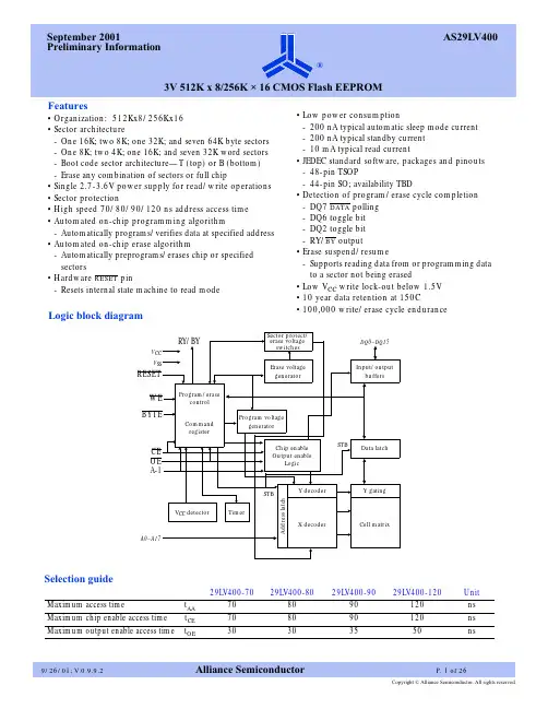
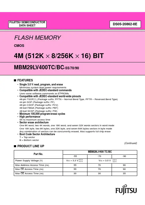
FEATURES• Single power supply operation- Full voltage range: 2.7 to 3.6 volts for read, erase and program operations• Low power cons umption (typical values at 5 MHz)- 9 mA typical active read current- 20 mA typical program/erase current- Less than 1 μA current in standby or automatic sleep mode.• JEDEC standards compatible- Pinout and software compatible with single-power supply Flash standard• Manufactured on 0.18μm process technology• Flexible Sector Architecture:- One hundred and twenty-eight 32K-Word /64K-byte sectors.• Minimum 100K program/erase endurance cycles.• High performance for program and erase - Word program time: 8µs typical - Sector Erase time: 500ms typical - Chip Erase time: 64s typical • Package Options - 48-pin TSOP - 48-ball FBGASoftware features: • Sector Group Protection- Provide locking of sectors to prevent program or erase operations within individual sectors - Additionally, temporary Sector GroupUnprotect allows code changes in previously protected sectors. • Standard DATA# polling and toggle bits feature• Unlock Bypass Program command supported • Sector Erase Suspend / Resume modes: Read and program another Sector during Sector Erase Suspend Mode• Support JEDEC Common Flash Interface (CFI).Hardware features:• Pin compatible to lower density, easy replacement for code expansion. • RESET# hardware reset pin- Hardware method to reset the device to read mode. • WP#/ACC input pin- Write Protect (WP#) function allowsprotection of first or last 32K-word sector, regardless of previous sector protect status - Acceleration (ACC) function provides accelerated program timesGENERAL DESCRIPTIONThe EN29LV640H/L / EN29LV640U is a 64-Megabit ( 4Mx16 ), electrically erasable, read/write non-volatile flash memory. Any word can be programmed typically in 8µs. This device is entirely command set compatible with the JEDEC single-power-supply Flash standard.The EN29LV640H/L / EN29LV640U is designed to allow either single Sector or full Chip erase operation, where each Sector Group can be protected against program/erase operations or temporarily unprotected to erase or program. The device can sustain a minimum of 100K program/erase cycles on each Sector.EN29LV640 64 Megabit (4M x 16-bit ) CMOS 3.0 Volt-only, Uniform Sector Flash MemoryPRODUCT SELECTOR GUIDEProduct Number EN29LV640H/LEN29LV640USpeed OptionFull Voltage Range: V CC =2.7 – 3.6 V90 90 Max Access Time (ns) 90 90 Max CE# Access Time (ns) 90 90 Max OE# Access Time (ns) 3535BLOCK DIAGRAMWE# CE# OE#State ControlCommand RegisterErase Voltage GeneratorInput/Output BuffersProgram Voltage GeneratorChip Enable Output EnableLogicData LatchY-Decoder X-Decoder Y-GatingCell MatrixTimerV CC DetectorA21-A0V CC V SS DQ15-DQ0Address LatchSector Protect SwitchesSTBSTBWP#/ ACC RY/BY#RESET#CONNECTION DIAGRAMSTABLE 1. PIN DESCRIPTIONLOGIC DIAGRAMDQ15 – DQ0A21 – A0WE#CE#RY/BY#OE#RESET#WP# / ACCPin Name Function A21-A0 22 Address inputs DQ15-DQ0 16 Data Inputs/Outputs CE# Chip Enable Input OE# Output Enable Input WE#Write Enable InputWP#/ACC Write Protect / Acceleration Pin RY/BY# Ready/Busy status output RESET# Hardware Reset Input Pin V cc Supply Voltage (2.7-3.6V) V ss GroundNCNot Connected to anythingORDERING INFORMATIONEN29LV640 H ─90 T C PPACKAGING CONTENT(Blank) = ConventionalP = Pb FreeTEMPERATURE RANGEI = Industrial (-40°C to +85°C)C = Commercial (0°C to +70°C)PACKAGET = 48-pin TSOPB = 48-Ball Fine Pitch Ball Grid Array (FBGA)0.80mm pitchSPEED OPTIONSee Product Selector Guide and Valid CombinationsSECTOR for WRITE PROTECT (WP#/ACC=0)H=highestaddresssectorprotectedL=lowestaddresssectorprotectedBASE PART NUMBEREN29LV640 / EN29LV640U64 Megabit(4M x 16-Bit) Uniform Sector Flash3V Read, Erase and ProgramPRODUCT SELECTOR GUIDEValid Combinations VccEN29LV640H–90 EN29LV640L–90 TI, TCBI,BCV cc = 2.7V-3.6VTable 2. Sector (Group) Address Tables Sector GroupProtect/UnprotectSector Address Range for Sector EraseSector Group A21-A17 Sector A21A20A19A18A17A16A15Address Range(hexadecimal) SA0 0 0 0 0 0 0 0 000000–007FFFSA1 0 0 0 0 0 0 1 008000–00FFFFSA2 0 0 0 0 0 1 0 010000–017FFFSG0 00000SA3 0 0 0 0 0 1 1 018000–01FFFFSA4 0 0 0 0 1 0 0 020000–027FFFSA5 0 0 0 0 1 0 1 028000–02FFFFSA6 0 0 0 0 1 1 0 030000–037FFF SG100001SA7 0 0 0 0 1 1 1 038000–03FFFFSA8 0 0 0 1 0 0 0 040000–047FFFSA9 0 0 0 1 0 0 1 048000–04FFFFSA10 0 0 0 1 0 1 0 050000–057FFF SG200010SA11 0 0 0 1 0 1 1 058000–05FFFFSA12 0 0 0 1 1 0 0 060000–067FFFSA13 0 0 0 1 1 0 1 068000–06FFFFSA14 0 0 0 1 1 1 0 070000–077FFF SG300011SA15 0 0 0 1 1 1 1 078000–07FFFFSA16 0 0 1 0 0 0 0 080000–087FFFSA17 0 0 1 0 0 0 1 088000–08FFFFSA18 0 0 1 0 0 1 0 090000–097FFF SG4 00100SA19 0 0 1 0 0 1 1 098000–09FFFFSA20 0 0 1 0 1 0 0 0A0000–0A7FFFSA21 0 0 1 0 1 0 1 0A8000–0AFFFFSA22 0 0 1 0 1 1 0 0B0000–0B7FFF SG5 00101SA23 0 0 1 0 1 1 1 0B8000–0BFFFFSA24 0 0 1 1 0 0 0 0C0000–0C7FFFSA25 0 0 1 1 0 0 1 0C8000–0CFFFFSA26 0 0 1 1 0 1 0 0D0000–0D7FFF SG6 00110SA27 0 0 1 1 0 1 1 0D8000–0DFFFFSA28 0 0 1 1 1 0 0 0E0000–0E7FFFSA29 0 0 1 1 1 0 1 0E8000–0EFFFFSA30 0 0 1 1 1 1 0 0F0000–0F7FFF SG700111SA31 0 0 1 1 1 1 1 0F8000–0FFFFFSector Group A21-A17 Sector A21 A20A19A18A17A16A15Address Range(hexadecimal) SA32 0 1 0 0 0 0 0 100000–107FFFSA33 0 1 0 0 0 0 1 108000–10FFFFSA34 0 1 0 0 0 1 0 110000–117FFFSG8 01000SA35 0 1 0 0 0 1 1 118000–11FFFFSA36 0 1 0 0 1 0 0 120000–127FFFSA37 0 1 0 0 1 0 1 128000–12FFFFSA38 0 1 0 0 1 1 0 130000–137FFF SG9 01001SA39 0 1 0 0 1 1 1 138000–13FFFFSA40 0 1 0 1 0 0 0 140000–147FFFSA41 0 1 0 1 0 0 1 148000–14FFFFSA42 0 1 0 1 0 1 0 150000–157FFF SG10 01010SA43 0 1 0 1 0 1 1 158000–15FFFFSA44 0 1 0 1 1 0 0 160000–167FFFSA45 0 1 0 1 1 0 1 168000–16FFFFSA46 0 1 0 1 1 1 0 170000–177FFF SG11 01011SA47 0 1 0 1 1 1 1 178000–17FFFFSA48 0 1 1 0 0 0 0 180000–187FFFSA49 0 1 1 0 0 0 1 188000–18FFFFSA50 0 1 1 0 0 1 0 190000–197FFF SG12 01100SA51 0 1 1 0 0 1 1 198000–19FFFFSA52 0 1 1 0 1 0 0 1A0000–1A7FFFSA53 0 1 1 0 1 0 1 1A8000–1AFFFFSA54 0 1 1 0 1 1 0 1B0000–1B7FFF SG13 01101SA55 0 1 1 0 1 1 1 1B8000–1BFFFFSA56 0 1 1 1 0 0 0 1C0000–1C7FFFSA57 0 1 1 1 0 0 1 1C8000–1CFFFFSA58 0 1 1 1 0 1 0 1D0000–1D7FFF SG14 01110SA59 0 1 1 1 0 1 1 1D8000–1DFFFFSA60 0 1 1 1 1 0 0 1E0000–1E7FFFSA61 0 1 1 1 1 0 1 1E8000–1EFFFFSA62 0 1 1 1 1 1 0 1F0000–1F7FFF SG15 01111SA63 0 1 1 1 1 1 1 1F8000–1FFFFFSector Group A21-A17 Sector A21A20A19A18A17A16A15Address Range(hexadecimal) SA64 1 0 0 0 0 0 0 200000–207FFFSA65 1 0 0 0 0 0 1 208000–20FFFFSA66 1 0 0 0 0 1 0 210000–217FFFSG16 10000SA67 1 0 0 0 0 1 1 218000–21FFFFSA68 1 0 0 0 1 0 0 220000–227FFFSA69 1 0 0 0 1 0 1 228000–22FFFFSA70 1 0 0 0 1 1 0 230000–237FFF SG1710001SA71 1 0 0 0 1 1 1 238000–23FFFFSA72 1 0 0 1 0 0 0 240000–247FFFSA73 1 0 0 1 0 0 1 248000–24FFFFSA74 1 0 0 1 0 1 0 250000–257FFF SG1810010SA75 1 0 0 1 0 1 1 258000–25FFFFSA76 1 0 0 1 1 0 0 260000–267FFFSA77 1 0 0 1 1 0 1 268000–26FFFFSA78 1 0 0 1 1 1 0 270000–277FFF SG1910011SA79 1 0 0 1 1 1 1 278000–27FFFFSA80 1 0 1 0 0 0 0 280000–287FFFSA81 1 0 1 0 0 0 1 288000–28FFFFSA82 1 0 1 0 0 1 0 290000–297FFF SG2010100SA83 1 0 1 0 0 1 1 298000–29FFFFSA84 1 0 1 0 1 0 0 2A0000–2A7FFFSA85 1 0 1 0 1 0 1 2A8000–2AFFFFSA86 1 0 1 0 1 1 0 2B0000–2B7FFF SG2110101SA87 1 0 1 0 1 1 1 2B8000–2BFFFFSA88 1 0 1 1 0 0 0 2C0000–2C7FFFSA89 1 0 1 1 0 0 1 2C8000–2CFFFFSA90 1 0 1 1 0 1 0 2D0000–2D7FFF SG2210110SA91 1 0 1 1 0 1 1 2D8000–2DFFFFSA92 1 0 1 1 1 0 0 2E0000–2E7FFFSA93 1 0 1 1 1 0 1 2E8000–2EFFFFSA94 1 0 1 1 1 1 0 2F0000–2F7FFF SG2310111SA95 1 0 1 1 1 1 1 2F8000–2FFFFFSector Group A21-A17 Sector A21A20A19A18A17A16A15Address Range(hexadecimal) SA96 1 1 0 0 0 0 0 300000–307FFFSA97 1 1 0 0 0 0 1 308000–30FFFFSA98 1 1 0 0 0 1 0 310000–317FFFSG24 11000SA99 1 1 0 0 0 1 1 318000–31FFFFSA100 1 1 0 0 1 0 0 320000–327FFFSA101 1 1 0 0 1 0 1 328000–32FFFFSA102 1 1 0 0 1 1 0 330000–337FFF SG25 11001SA103 1 1 0 0 1 1 1 338000–33FFFFSA104 1 1 0 1 0 0 0 340000–347FFFSA105 1 1 0 1 0 0 1 348000–34FFFFSA106 1 1 0 1 0 1 0 350000–357FFF SG26 11010SA107 1 1 0 1 0 1 1 358000–35FFFFSA108 1 1 0 1 1 0 0 360000–367FFFSA109 1 1 0 1 1 0 1 368000–36FFFFSA110 1 1 0 1 1 1 0 370000–377FFF SG27 11011SA111 1 1 0 1 1 1 1 378000–37FFFFSA112 1 1 1 0 0 0 0 380000–387FFFSA113 1 1 1 0 0 0 1 388000–38FFFFSA114 1 1 1 0 0 1 0 390000–397FFF SG28 11100SA115 1 1 1 0 0 1 1 398000–39FFFFSA116 1 1 1 0 1 0 0 3A0000–3A7FFFSA117 1 1 1 0 1 0 1 3A8000–3AFFFFSA118 1 1 1 0 1 1 0 3B0000–3B7FFF SG29 11101SA119 1 1 1 0 1 1 1 3B8000–3BFFFFSA120 1 1 1 1 0 0 0 3C0000–3C7FFFSA121 1 1 1 1 0 0 1 3C8000–3CFFFFSA122 1 1 1 1 0 1 0 3D0000–3D7FFF SG30 11110SA123 1 1 1 1 0 1 1 3D8000–3DFFFFSA124 1 1 1 1 1 0 0 3E0000–3E7FFFSA125 1 1 1 1 1 0 1 3E8000–3EFFFFSA126 1 1 1 1 1 1 0 3F0000–3F7FFF SG31 11111SA127 1 1 1 1 1 1 1 3F8000–3FFFFF Note: The sizes of all sectors are 32K-word.USER MODE DEFINITIONSTABLE 3. BUS OPERATIONSOperation CE#OE#WE#RESET#WP#/ACC A21-A0DQ15-DQ0 Read LLHHL/HA IN D OUTWrite LHLH(Note1)A IN(Note 3)AcceleratedProgramL H L H V HH A IN(Note 3)CMOS Standby V cc±0.3V X X V cc±0.3VH XHigh-ZTTL Standby H X X H L / H X High-Z Output Disable L H H H L / H X High-Z Hardware Reset X X X L L / H X High-ZSector Group Protect (Note 2) L H L V ID HSA,A6=L,A1=H,A0=L(Note 3)Sector GroupUnprotect (Note 2) L H L V ID HSA,A6=H,A1=H,A0=L(Note 3)TemporarySector GroupUnprotectX X X V ID H A IN(Note 3)L=logic low= V IL, H=Logic High= V IH, V ID= V HH = 11 ± 0.5V = 10.5 ─ 11.5V, X=Don’t Care (eitherL or H, but not floating!), SA=Sector Addresses (A21-A15), D IN=Data In, D OUT=Data Out,A IN=Address InNotes:1. If the system asserts V IL on the WP# / ACC pin, the device disables program and erasefunctions in the first or last sector independent of whether those sectors were protected orunprotected; if the system asserts V IH on the WP# /ACC pin, the device reverts to whether thefirst or last sector was previously protected or unprotected. If WP# / ACC = V HH, all sectors willbe unprotected.2. Please refer to “Sector Group Protection & Unprotection”, Flowchart 6a and Flowchart 6b.3. D IN or D OUT as required by command sequence, data polling, or sector protect algorithm.Read ModeThe device is automatically set to reading array data after device power-up or hardware reset. No commands are required to retrieve data. The device is also ready to read array data after completing an Embedded Program or Embedded Erase algorithmAfter the device accepts an Sector Erase Suspend command, the device enters the Sector Erase Suspend mode. The system can read array data using the standard read timings, except that if it reads at an address within erase-suspended sectors, the device outputs status data. After completing aprogramming operation in the Sector Erase Suspend mode, the system may once again read array data with the same exception. See “Sector Erase Suspend/Resume Commands” for more additional information.The system must issue the reset command to re-enable the device for reading array data if DQ5 goes high or while in the autoselect mode. See the “Reset Command” for additional details.Output Disable ModeWhen the OE# pin is at a logic high level (V IH), the output from the device is disabled. The output pins are placed in a high impedance state.Standby ModeThe device has a CMOS-compatible standby mode, which reduces the c urrent to < 1µA (typical). It is placed in CMOS-compatible standby when the CE# pin is at V CC± 0.5. RESET# and BYTE# pin must also be at CMOS input levels. The device also has a TTL-compatible standby mode, which reduces the maximum V CC c urrent to < 1mA. It is placed in TTL-compatible standby when the CE# pin is at V IH. When in standby modes, the outputs are in a high-impedance state independent of the OE# input.Automatic Sleep ModeThe device has an automatic sleep mode, which minimizes power consumption. The devices will enter this mode automatically when the states of address bus remain stable for t acc + 30ns. ICC4 in the DC Characteristics table shows the current specification. With standard access times, the device will output new data when addresses change.Writing Command SequencesTo write a command or command sequence to program data to the device or erase data, the system has to drive WE# and CE# to V IL, and OE# to V IH.The device has an Unlock Bypass mode to facilitate faster programming. Once the device enters the Unlock Bypass mode, only two write cycles are required to program a word, instead of four.The system can also read the autoselect codes by entering the autoselect mode, which need the autoselect command sequence to be written. Please refer to the “Command Definitions” for all the available commands.Autoselect Identification ModeThe autoselect mode provides manufacturer and device identification, and sector protection verification, through identifier codes output on DQ15–DQ0. This mode is primarily intended for programming equipment to automatically match a device to be programmed with its corresponding programming algorithm. However, the autoselect codes can also be accessed in-system through the command register.When using programming equipment, the autoselect mode requires V ID(10.5 V to 11.5 V) on address pin A9. Address pins A6, A1, and A0 must be as shown in Autoselect Codes table. In addition, when verifying sector group protection, the sector group address must appear on the appropriate highest order address bits. Refer to the corresponding Sector Address Tables. The “Command Definitions” table shows the remaining address bits that are don’t-care. When all necessary bits have been set as required, the programming equipment may then read the corresponding identifier code on DQ15–DQ0. To access the autoselect codes in-system; the host system can issue the autoselect command via the command register, as shown in the Command Definitions table. This method does not require V ID. See“Command Definitions” for details on using the autoselect mode. Note that a Reset command is required to return to read mode when the device is in the autoselect mode.TABLE 4. Autoselect Codes (Using High Voltage, V ID )L=logic low= V IL , H=Logic High= V IH , V ID =11 ± 0.5V, X=Don’t Care (either L or H, but not floating!), SA=Sector AddressesNote:1. A8=H is recommended for Manufacturing ID check. If a manufacturing ID is read with A8=L, the chip will output a configuration code 7Fh.2. A9 = V ID is for HV A9 Autoselect mode only. A9 must be ≤ Vcc (CMOS logic level) for Command AutoselectMode.RESET#: Hardware ResetWhen RESET# is driven low for t RP , all output pins are tristates. All commands written in the internal state machine are reset to reading array data.Please refer to timing diagram for RESET# pin in “AC Characteristics”.Sector Group Protection & UnprotectionThe hardware sector group protection feature disables both program and erase operations in any sector group. The hardware chip unprotection feature re-enables both program and erase operations in previously protected sector group. A sector group consists of four adjacent sectors that would be protected at the same time. Please see Table 2 which show the organization of sector groups.There are two methods to enable this hardware protection circuitry. The first one requires only that the RESET# pin be at V ID and then standard microprocessor timings can be used to enable or disable this feature. See Flowchart 6a and 6b for the algorithm and Figure 11 for the timings.When doing Sector Group Unprotect, all the unprotected sector groups must be protected prior to any unprotect write cycle.The second method is for programming equipment. This method requires V ID to be applied to both OE# and A9 pins and non-standard microprocessor timings are used. This method is described in a separate document, the Datasheet Supplement of EN29LV640H/L ; EN29LV640U, which can be obtained by contacting a representative of Eon Silicon Solution, Inc.Description CE# OE# WE# A21toA15 A14 to A10A92A8A7A6A5 to A2A1 A0 DQ15 to DQ0H1XX1Ch Manufacturer ID: Eon L L H X X V IDLX L XL LXX7FhAutoselect Device ID L L H X X V IDX X L X L H 227Eh Sector Protection VerificationL L H SA X V IDX X L X H LXX01h(Protected)XX00h(Unprotected)Write Protect / Accelerated Program (WP# / ACC)The Write Protect function provides a hardware method to protect the first or last sector against erase and program without using V ID.When WP# is Low, the device protects the first or last sector regardless of whether these sectors were previously protected or unprotected using the method described in “Sector Group Protection & Unprotection”, Program and Erase operations in these sectors are ignored.When WP# is High, the device reverts to the previous protection status of the first or last sector. Program and Erase operations can now modify the data in those sectors unless the sector is protected using Sector Group Protection.Note that the WP# pin must not be left floating or unconnected.When WP#/ACC is raised to V HH the memory automatically enters the Unlock Bypass mode(please refer to “Command Definitions”), temporarily unprotects every protected sectors, and reduces the time required for program operation. The system would use a two-cycle program command sequence as required by the Unlock Bypass mode. When WP#/ACC returns to V IH or V IL, normal operation resumes. The transitions from V IH or V IL to V HH and from V HH to V IH or V IL must be slower than t V HH, see Figure 5. Note that the WP#/ACC pin must not be left floating or unconnected. In addition, WP#/ACC pin mustnot be at V HH for operations other than accelerated programming. It could cause the device to be damaged.Never raise this pin to V HH from any mode except Read mode, otherwise the memory may be left in an indeterminate state.A 0.1µF capacitor should be connected between the WP#/ACC pin and the VSS Ground pin to decouple the current surges from the power supply. The PCB track widths must be sufficient to carry the currents required during Unlock Bypass Program.Temporary Sector Group UnprotectThis feature allows temporary unprotection of previously protected sector groups to change data while in-system. The Temporary Sector Group Unprotect mode is activated by setting the RESET# pin to V I D. During this mode, formerly protected sector groups can be programmed or erased by simply selecting the sector group addresses. Once V I D is removed from the RESET# pin, all the previously protected sector groups are protected again. See accompanying flowchart and timing diagrams in Figure 10 for more details.StartReset#=V ID(note 1) Perform Erase or ProgramOperationsRESET#=V IH Temporary Sector Group Unprotect Completed (note 2)Notes:1. All protected sector groups are unprotected. (If WP#/ACC=V IL, the first or last sector will remain protected.)2. Previously protected sector groups are protected again.COMMON FLASH INTERFACE (CFI)The common flash interface (CFI) specification outlines device and host systems software interrogation handshake, which allows specific vendor-specified software algorithms to be used for entire families of devices. Software support can then be device-independent, JEDEC ID-independent, and forward- and backward-compatible for the specified flash device families. Flash vendors can standardize their existing interfaces for long-term compatibility.This device enters the CFI Query mode when the system writes the CFI Query command, 98h, to address 55h, any time the device is ready to read array data.The system can read CFI information at the addresses given in Tables 5-8.The upper address bits (A7–MSB) must be all zeros. To terminate reading CFI data, the system must write the reset command.The system can also write the CFI query command when the device is in the autoselect mode. The device enters the CFI query mode and the system can read CFI data at the addresses given in Tables 5–8. The system must write the reset command to return the device to the autoselect mode.Table 5. CFI Query Identification StringAddresses Data Description10h 11h 12h 0051h0052h0059hQuery Unique ASCII string “QRY”13h 14h 0002h0000hPrimary OEM Command Set15h 16h 0040h0000hAddress for Primary Extended Table17h 18h 0000h0000hAlternate OEM Command set (00h = none exists)19h 1Ah 0000h0000hAddress for Alternate OEM Extended Table (00h = none exists)Table 6. System Interface StringAddresses Data Description1Bh 0027h Vcc Min (write/erase)DQ7-DQ4: volt, DQ3 –DQ0: 100 millivolt1Ch 0036h Vcc Max (write/erase)DQ7-DQ4: volt, DQ3 –DQ0: 100 millivolt1Dh 0000h Vpp Min. voltage (00h = no Vpp pin present)1Eh 0000h Vpp Max. voltage (00h = no Vpp pin present)1Fh 0003h Typical timeout per single byte/word write 2NμS20h 0000h Typical timeout for Min, size buffer write 2NμS (00h = not supported) 21h 000Ah Typical timeout per individual block erase 2N ms22h 0000h Typical timeout for full chip erase 2N ms (00h = not supported)23h 0005h Max. timeout for byte/word write 2N times typical24h 0000h Max. timeout for buffer write 2N times typical25h 0002h Max. timeout per individual block erase 2N times typical26h 0000h Max timeout for full chip erase 2N times typical (00h = not supported)Table 7. Device Geometry DefinitionAddresses Data Description27h 0017h Device Size = 2Nbytes 28h 29h 0001h0000h Flash Device Interface description (refer to CFI publication 100)2Ah 2Bh 0000h 0000h Max. number of byte in multi-byte write = 2N (00h = not supported) 2Ch 0001h Number of Erase Block Regions within device 2Dh 2Eh 2Fh 30h 007Fh 0000h 0000h 0001h Erase Block Region 1 Information (refer to the CFI specification of CFI publication 100) 31h 32h 33h 34h 0000h 0000h0000h 0000h Erase Block Region 2 Information35h 36h 37h 38h 0000h 0000h0000h 0000h Erase Block Region 3 Information39h 3Ah 3Bh 3Ch 0000h 0000h0000h 0000hErase Block Region 4 InformationTable 8. Primary Vendor-specific Extended QueryAddresses Data Description40h 41h 42h 0050h 0052h 0049h Query-unique ASCII string “PRI” 43h 0031h Major version number, ASCII 44h 0033h Minor version number, ASCII45h 0004hAddress Sensitive Unlock0 = Required, 1 = Not Required 46h 0002hErase Suspend0 = Not Supported, 1 = To Read Only, 2 = To Read & Write 47h 0004hSector Protect0 = Not Supported, X = Number of sectors in per group 48h 0001hSector Temporary Unprotect00 = Not Supported, 01 = Supported 49h 0004h Sector Protect/Unprotect scheme01 = 29F040 mode, 02 = 29F016 mode,03 = 29F400 mode, 04 = 29LV800A mode 4Ah 0000hSimultaneous Operation00 = Not Supported, 01 = Supported 4Bh 0000hBurst Mode Type00 = Not Supported, 01 = Supported 4Ch 0000hPage Mode Type00 = Not Supported, 01 = 4 Word Page, 02 = 8 Word Page 4Dh 00A5hMinimum WP#/ACC (Acceleration) Supply Voltage00 = Not Supported, DQ7-DQ4 : Volts, DQ3-DQ0 : 100mV 4Eh 00B5hMaximum WP#/ACC (Acceleration) Supply Voltage00 = Not Supported, DQ7-DQ4 : Volts, DQ3-DQ0 : 100mV4Fh 00XXh 00h = Uniform Sector DevicesHardware Data protectionThe command sequence requirement of unlock cycles for programming or erasing provides data protection against inadvertent writes as seen in the Command Definitions table. Additionally, the following hardware data protection measures prevent accidental erasure or programming, which might otherwise be caused by false system level signals during Vcc power up and power down transitions, or from system noise.Low V CC Write InhibitWhen V CC is less than V LKO, the device does not accept any write cycles. This protects data during V CC power up and power down. The command register and all internal program/erase circuits are disabled, and the device resets. Subsequent writes are ignored until V CC is greater than V LKO. The system must provide the proper signals to the control pins to prevent unintentional writes when V CC is greater than V LKO.Write Pulse “Glitch” protectionNoise pulses of less than 5 ns (typical) on OE#, CE# or WE# do not initiate a write cycle.Logical InhibitWrite cycles are inhibited by holding any one of OE# = V IL, CE# = V IH, or WE# = V IH. To initiate a write cycle, CE# and WE# must be a logical zero while OE# is a logical one. If CE#, WE#, and OE# are all logical zero (not recommended usage), it will be considered a read.Power-up Write InhibitDuring power-up, the device automatically resets to READ mode and locks out write cycles. Even with CE# = V IL, WE#= V IL and OE# = V IH, the device will not accept commands on the rising edge of WE#.COMMAND DEFINITIONSThe operations of the device are selected by one or more commands written into the commandregister. Commands are made up of data sequences written at specific addresses via the command register. The sequences for the specified operation are defined in the Command Definitions table (Table 9). Incorrect addresses, incorrect data values or improper sequences will reset the device to Read Mode.Table 9. EN29LV640H/L / EN29LV640U Command DefinitionsBus Cycles (Note 1-2)1stCycle 2ndCycle3rdCycle4thCycle5thCycle6thCycleCommand Sequence C y c l e sAddr DataAddr DataAddr DataAddr DataAddr DataAddr DataRead (Note 3)1RA RD Reset 1xxx F0 Manufacturer ID 4555 AA 2AA 55 55590000 1007F 1CDevice ID 4555 AA 2AA 55 55590 X01 227E A u t o s e l e c tSector Protect Verify (Note 4)4555 AA 2AA 55 55590(SA)X02XX00 XX01Program 4555 AA 2AA 55 555A0 PA PD Unlock Bypass 3555 AA 2AA 55 55520 Unlock Bypass Program2XXX A0 PA PD Unlock Bypass Reset 2XXX90XXX00Chip Erase 6555 AA 2AA 55 55580 555 AA 2AA 55 55510Sector Erase 6555 AA 2AA 55 55580 555 AA 2AA 55 SA 30 Sector Erase Suspend 1BA B0 Sector Erase Resume 1BA 30 CFI Query 15598Address and Data values indicated are in hex. Unless specified, all bus cycles are write cycles RA = Read Address: address of the memory location to be read. This is a read cycle. RD = Read Data: data read from location RA during Read operation. This is a read cycle. PA = Program Address: address of the memory location to be programmed. X = Don’t-Care PD = Program Data: data to be programmed at location PASA = Sector Address: address of the Sector to be erased or verified (in Autoselect mode).Address bits A21-A15 uniquely select any Sector.Notes:1. Data bits DQ15-DQ8 are don’t care in command sequences, except for RD and PD.2. Unless otherwise noted, address bits A21-A15 are don’t cares.3. No unlock or command cycles required when device is in read mode.4. The data is 00h for an unprotected sector group and 01h for a protected sector group.。