lab3_VHDL
- 格式:pdf
- 大小:147.30 KB
- 文档页数:7
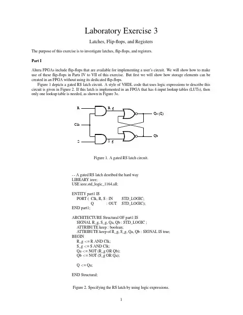
Laboratory Exercise 3Latches, Flip-flops, and RegistersThe purpose of this exercise is to investigate latches, flip-flops, and registers.Part IAltera FPGAs include flip-flops that are available for implementing a user’s circuit. We will show how to make use of these flip-flops in Parts IV to VII of this exercise. But first we will show how storage elements can be created in an FPGA without using its dedicated flip-flops.Figure 1 depicts a gated RS latch circuit. A style of VHDL code that uses logic expressions to describe this circuit is given in Figure 2. If this latch is implemented in an FPGA that has 4-input lookup tables (LUTs), then only one lookup table is needed, as shown in Figure 3a.Figure 1.A gated RS latch circuit.1Figure 2.Specifying the RS latch by using logic expressions.Although the latch can be correctly realized in one 4-input LUT, this implementation does not allow its internal signals, such as R_g and S _g, to be observed, because they are not provided as outputs from the LUT. To preserve these internal signals in the implemented circuit, it is necessary to include a compiler directive in the code. In Figure 2 the directive keep is included by using a VHDL ATTRIBUTE statement; it instructs the Quartus II compiler to use separate logic elements for each of the signals R_g, S_g,Qa, and Qb. Compiling the code produces the circuit with four 4-LUTs depicted in Figure 3b.(a) Using one 4-input lookup table for the RS latch.2(b) Using four 4-input lookup tables for the RS latch.Figure 3.Implementation of the RS latch from Figure 1.Create a Quartus II project for the RS latch circuit as follows:1. Create a new project for the RS latch. Select as the target chip the Cyclone IVEP4CE115F29C8, which is the FPGA chip on the Altera DE2-115 board.2. Generate a VHDL file with the code in Figure 2 and include it in the project.3. Compile the code. Use the Quartus II RTL Viewer tool to examine the gate-level circuitproduced from the code, and use the Technology Viewer tool to verify that the latch is implemented as shown in Figure 3b.Part IIFigure 4 shows the circuit for a gated D latch.Figure 4.Circuit for a gated D latch.3Perform the following steps:1. Create a new Quartus II project. Generate a VHDL file using the style of code in Figure 2for the gated D latch. Use the keep directive to ensure that separate logic elements are used to implement the signals R, S_g, R_g,Qa, and Qb.2. Select as the target chip the Cyclone IV EP4CE115F29C8 and compile the code. Use theTechnology Viewer tool to examine the implemented circuit.3. Verify that the latch works properly for all input conditions by using functional simulation.Examine the timing characteristics of the circuit by using timing simulation.4. Create a new Quartus II project which will be used for implementation of the gated D latchon the DE2-115 board. This project should consist of a top-level entity that contains the appropriate input and output ports (pins) for the DE2-115 board. Instantiate your latch in this top-level entity. Use switch SW 0 to drive the D input of the latch, and use SW1 as the Clk input. Connect the Q output to LEDR 0.5. Recompile your project and download the compiled circuit onto the DE2-115 board.6. Test the functionality of your circuit by toggling the D and Clk switches and observing the Qoutput.Part IIIFigure 5 shows the circuit for a master-slave D flip-flop.Figure 5.Circuit for a master-slave D flip-flop.Perform the following:1. Create a new Quartus II project. Generate a VHDL file that instantiates two copies of yourgated D latch entity from Part II to implement the master-slave flip-flop.42. Include in your project the appropriate input and output ports for the Altera DE2-115 board.Use switch SW 0 to drive the D input of the flip-flop, and use SW 1 as the Clock input.Connect the Q output to LEDR0.3. Compile your project.4. Use the Technology Viewer to examine the D flip-flop circuit, and use simulation to verifyits correct operation.5. Download the circuit onto the DE2-115 board and test its functionality by toggling the Dand Clock switches and observing the Q output.Part IVFigure 6 shows a circuit with three different storage elements: a gated D latch, a positive-edge triggered D flip-flop, and a negative-edge triggered D flip-flop.(a) Circuit(b) Timing diagramFigure 6.Circuit and waveforms for Part IV.5Implement and simulate this circuit using Quartus II software as follows:1. Create a new project.2. Write a VHDL file that instantiates the three storage elements. For this part you should nolonger use the keep directive (that is, the VHDL ATTRIBUTE statement) from Parts I to III.Figure 7 gives a behavioral style of VHDL code that specifies the gated D latch in Figure 4.This latch can be implemented in one 4-input lookup table. Use a similar style of code to specify the flip-flops in Figure 6.3. Compile your code and use the Technology Viewer to examine the implemented circuit.Verify that the latch uses one lookup table and that the flip-flops are implemented using the flip-flops provided in the target FPGA.Figure 7.A behavioral style of VHDL code that specifies a gated D latch.6Part VWe wish to display the hexadecimal value of a 16-bit number A on the four 7-segment displays, HEX7 − 4. We also wish to display the hex value of a 16-bit number B on the four 7-segment displays, HEX3 − 0. The values of A and B are inputs to the circuit which are provided by means of switches SW15−0. This is to be done by first setting the switches to the value of A and then setting the switches to the value of B; therefore, the value of A must be stored in the circuit.1. Create a new Quartus II project which will be used to implement the desired circuit on theAltera DE2-115 board.2. Write a VHDL file that provides the necessary functionality. Use KEY 0 as an active-lowasynchronous reset, and use KEY1 as a clock input. Include the VHDL file in your project and compile the circuit.3. Assign the pins on the FPGA to connect to the switches and 7-segment displays, asindicated in the User Manual for the DE2-115 board.4. Recompile the circuit and download it into the FPGA chip.5. Test the functionality of your design by toggling the switches and observing the outputdisplays.Copyright ○c2010 Altera Corporation.7。