st485e 非常稳定的485芯片
- 格式:pdf
- 大小:698.78 KB
- 文档页数:18
485 芯片485芯片是一种用于嵌入式系统的通信和控制芯片,具有高性能、低功耗、可靠性高等特点。
下面将对485芯片的特点、应用领域和工作原理进行详细的介绍。
485芯片的特点:1. 高性能:485芯片具有高速的数据传输能力,传输速度可达到10Mbps,支持同时接入多个设备进行通信。
2. 低功耗:485芯片采用低功耗的设计,可以在工作状态下仅消耗数毫瓦的功率。
3. 可靠性高:485芯片采用差分信号传输模式,具有很强的抗干扰能力,可以在恶劣的环境下稳定工作。
4. 节约成本:由于485芯片支持多个设备同时接入,可以减少系统中所需的通信线路,降低成本。
5. 简化系统设计:485芯片具备自动流控和自动方向控制功能,可以减少外围电路的设计难度,简化系统设计。
485芯片的应用领域:1. 工业自动化:485芯片常用于工业控制系统中,如PLC、传感器、仪表、计量设备等的通信和控制。
2. 智能家居:485芯片可以用于智能家居设备之间的通信,如智能开关、温度控制器等。
3. 智能交通:485芯片可以用于交通信号灯、道路监控、车辆检测等系统的通信和控制。
4. 智能电网:485芯片可以用于电力系统的远程监控和控制,如变电站、配电设备、能耗检测等。
485芯片的工作原理:485芯片采用差分信号传输模式,数据通信是通过正负两个信号线来实现的。
其中,正线为数据线,负线为数据线的反向线。
通过差分信号的方式可以大大提高抗干扰能力,使得数据传输更加稳定可靠。
485芯片工作时分为发送和接收两个阶段:1. 发送:当发送端要发送数据时,数据经过发送驱动电路转换成差分信号,并通过正线和负线传输到接收端。
2. 接收:接收端的芯片接收到差分信号后,将差分信号转换成数据,并通过接收电路输出给外部设备。
在485系统中,可以布置多个设备共享同一条通信线路,各个设备之间通过地址进行区分,只有接收到相应地址的数据才会进行处理。
总之,485芯片是一种功能强大、稳定可靠的通信和控制芯片,广泛应用于工业自动化、智能家居、智能交通、智能电网等领域。
485隔离芯片隔离芯片是一种电子器件,在电路设计中具有非常重要的作用。
它用于在不同的电路之间提供电气隔离,防止电流、信号等在电路之间相互影响或传递,从而实现电路之间的安全隔离。
隔离芯片一般由隔离转换器、输入输出电路和供电电路等组成。
它的工作原理是通过电绝缘技术,将输入信号从输入电路中转换成光、磁、电容等其他形式的信号,然后再通过输出电路将信号转换回来。
这样一来,输入电路和输出电路之间就不存在任何的电气连接,实现了电力的隔离。
隔离芯片广泛应用于各种领域,特别是在工业自动化、电力电子、通信等领域。
其中,最常见的应用就是在工业自动化领域,用于保护工业设备和人身安全。
由于工业环境中存在很高的电压、电流等危险因素,为了保护设备和人员的安全,必须将电路进行隔离,以防止危险因素对其他电路产生影响。
隔离芯片的优势是它能够实现高电压、高电流的隔离,同时能够在宽工作温度范围内正常工作。
此外,隔离芯片的体积小、重量轻、功耗低,能够满足各种特殊环境的需求。
另外,隔离芯片还具有高抗干扰性、高精度、高可靠性等优点。
然而,隔离芯片也存在一些问题需要解决。
首先是成本问题,隔离芯片的价格相对较高,对于一些低成本的电子产品来说可能会增加产品的成本。
其次,隔离芯片的隔离效果可能会受到一些外界因素的影响,比如温度、湿度等,这可能会影响隔离芯片的工作质量和可靠性。
综上所述,隔离芯片作为一种电子器件,在电路设计中发挥着非常重要的作用。
它通过电绝缘技术实现电路之间的隔离,保护了电路和设备的安全。
隔离芯片具有体积小、重量轻、功耗低等优点,同时也存在一些问题需要解决。
随着科技的不断进步,相信隔离芯片将会得到更广泛的应用,并不断发展和完善。
max485芯片MAX485是一种用于串行通讯的芯片,它可以实现半双工的通信,常用于RS-485网络中。
这款芯片具有低功耗、高速率、低电压、可靠性高等特点,被广泛应用于工业自动化、远程监控、数据采集等领域。
MAX485芯片采用了双绞四线制接口,可以实现长距离传输,通信距离可达1200米。
其通信速率可以高达2.5Mbps,同时还支持多点连接,可以连接最多32个驱动器和接收器。
MAX485芯片的工作电压范围为3.0V至5.25V,因此可以适应不同的工作环境。
在低功耗模式下,它的供电电流仅为1μA,非常适合电池供电的应用。
此外,MAX485还具有过温保护功能,可以保护芯片免受过热损坏。
MAX485芯片的架构采用了低功耗CMOS技术,具有自动接收释放和禁用保护电路,可以有效地降低功耗。
此外,它还配备了过电流保护和过电压保护电路,可以保护芯片免受电路故障的影响。
MAX485芯片的引脚功能如下:- A/B:差分传输线,用于发送和接收数据。
- RE/DE:接收使能/发送使能引脚,用于控制芯片的发送和接收功能。
- RO/RE:发送使能/接收使能引脚,用于选择芯片的发送和接收功能。
- VCC:供电引脚,具有3.0V至5.25V的宽工作电压范围。
- GND:地线引脚,用于接地连接。
MAX485芯片的工作原理如下:- 发送数据时,通过RE/DE引脚将芯片设置为发送模式,将发送的数据信号输入到A/B差分传输线上。
- 接收数据时,通过RE/DE引脚将芯片设置为接收模式,通过RO/RE引脚选择芯片的发送和接收功能。
接收到的数据信号经过差分收发线转换为通用串行总线信号。
- 在半双工通信时,A/B线上只能有一方发送数据,另一方只能接收数据。
总之,MAX485芯片是一款功能强大且灵活的串行通信芯片,具有高速率、低功耗、可靠性高等特点,被广泛应用于工业自动化、远程监控、数据采集等领域。
它的性能优越和稳定性使得它成为RS-485通信领域中的首选芯片。
3485芯片3485芯片简介3485芯片是一种高集成度数字电路芯片,广泛应用于各种电子设备中。
该芯片采用先进的技术和制造工艺,具有高性能、高可靠性和低功耗等优点。
3485芯片主要包含逻辑电路、存储电路和控制电路等功能模块。
逻辑电路部分常见的包括与门、或门、非门以及与非门等,用于实现不同的逻辑运算。
存储电路部分则通常采用闪存或者SRAM等类型的存储器,用于存储程序和数据。
控制电路主要用于调度和控制各个功能模块的工作。
3485芯片具有以下特点:1. 高性能:3485芯片采用先进的制造工艺和设计技术,具有较高的工作频率和处理能力,能够满足复杂电子设备的性能要求。
2. 高可靠性:3485芯片采用先进的工艺和材料,具有较高的抗干扰和抗辐射能力,能够在复杂环境下稳定工作。
3. 低功耗:3485芯片采用先进的功耗优化技术,能够以较低的功耗运行,延长电池寿命和减少能量消耗。
4. 强大的扩展性:3485芯片支持多种外设接口和通信接口,可以方便地与其他设备进行连接和通信,实现更丰富的功能和应用。
5. 丰富的开发工具和支持:针对3485芯片,有众多的开发工具和软件支持,包括开发板、编译器、仿真器等,使得开发人员可以更加方便地进行软硬件开发和调试。
在实际应用中,3485芯片广泛被应用于各种电子设备中,例如智能手机、平板电脑、数字相机、无线路由器等。
它在提供强大功能和性能的同时,也满足了用户对于小型、轻便和低功耗的要求。
总结起来,3485芯片是一种高集成度、高性能、高可靠性、低功耗的数字电路芯片,广泛应用于各种电子设备中。
它的出现使得电子设备可以更加智能化、便捷化和高效化。
第2期Si m ul at i on research on speed adj ust i ng val ve cont rol l ed synchronous l i f t i ng syst em based on A m esi mW EI H ai t ao 1,2,W EI H ai f eng 3,ZH A N G X i aol i 1,M A Zhi gang 1,W A N G Shengj i n 1,2,Y A N G Zhi huai1,2(nz hou LS G r oup Co.,Lt d.Ener gy Equi pm ent R es ear ch I ns t i t ut e,Lanz hou 730314,G ans u Chi na;nz hou LS Ener gy Equi pm ent Engi neer i ng R es ear ch I ns t i t ut e Co.,Lt d.,Lanz hou 730314,G ans u Chi na;nz hou LS Pet r ol eum Equi pm ent Engi neer i ng Co.,Lt d.,Lanz hou 730314,G ans u Chi na )A bs t ract :The l i f t i ng s ys t em of s om e cer t ai n hi gh l egged vehi cl e r equi r es t he vehi cl e body t o achi eve s m oot hl i f t i ng and ens ur e s ynchr onous l i f t i ng.O t her wi s e,i t m ay cause dam age t o t he vehi cl e body or hydr aul i c cyl i n-der ,and even caus e ser i ous dam age t o t he over al l s t r uct ur e of t he hi gh l egged vehi cl e due t o t he unevennes s of t he vehi cl e body.H owever ,due t o t he f act t hat t he cent er of gr avi t y of t he vehi cl e body i s l ocat ed at t he l ef t r ear of t he vehi cl e body,and t he l oads on t he f our l i f t i ng cyl i nder s ar e not equal .I n or der t o ens ur e t he s ynchr oni z at i on of t he vehi cl e body l i f t i ng and l ower i ng,t he s i m ul at i on m odel s f or t he i nl et t hr ot t l e s peed ad-j us t i ng ci r cui t and out l et t hr ot t l e s peed adj us t i ng ci r cui t of t he l i f t i ng s yst em speed adj us t i ng val ve have been es t abl i s hed on t he bas i s of A m esi m si m ul at i on s of t war e i n t he t ext ,as wel l as t he i nl et t hr ot t l e s peed cont r ol ci r cui t of t he r i si ng s peed adj us t i ng val ve and t he out l et t hr ot t l e s peed cont r ol ci r cui t of t he des cendi ng s peed adj us t i ng val ve.The s t abi l i t y of pr es s ur e and speed as wel l as t he s ynchr oni ci t y of t he l i f t i ng and l ower i ng of t he hi gh l egged vehi cl e of t he t hr ee ci r cui t s have been com par ed and anal yz ed under di f f er ent l oadi ng of f our cyl i nder s.The r es ul t s s how t hat t he l i f t i ng s ys t em by us i ng of a s peed adj us t i ng val ve and r ect i f i er boar d,whi ch us es t he i nl et t hr ot t l e s peed cont r ol of t he s peed adj ust i ng val ve f or as cendi ng and t he out l et t hr ot t l e s peed cont r ol ci r cui t of t he s peed adj us t i ng val ve f or des cendi ng,has s t abl e pr es sur e and s peed,as wel l as good l i f t i ng s ynchr oni z at i on per f or m ance,pr ovi di ng a bas i s f or t he des i gn of t he s ynchr oni z at i on s ys t em.K ey w ords :Li f t i ng sys t em ;Synchr oni ci t y;Si m ul at i on;Speed adj us t i ng val ve;R ect i f i er boar d工业自动化控制实时数据传输系统是目前工业智能化发展的一个重要领域。
提高RS-485总线可靠性的几种方法及常见故障处理提高RS-485总线可靠性的几种方法及常见故障处理提高RS-485总线可靠性的几种方法及常见故障处理在MCU之间中长距离通信的诸多方案中,RS-485因硬件设计简单、控制方便、成本低廉等优点广泛应用于工厂自动化、工业控制、小区监控、水利自动报测等领域。
但RS-485总线在抗干扰、自适应、通信效率等方面仍存在缺陷,一些细节的处理不当常会导致通信失败甚至系统瘫痪等故障,因此提高RS-485总线的运行可靠性至关重要。
1 RS-485接口电路的硬件设计 1)总线匹配。
总线匹配有两种方法,一种是加匹配电阻,如图1a所示。
位于总线两端的差分端口VA与VB之间应跨接120Ω匹配电阻,以减少由于不匹配而引起的反射、吸收噪声,有效地抑制了噪声干扰。
但匹配电阻要消耗较大电流,不适用于功耗限制严格的系统。
另外一种比较省电的匹配方案是RC 匹配(图2 )利用一只电容C 隔断直流成分,可以节省大部分功率,但电容C 的取值是个难点,需要在功耗和匹配质量间进行折衷。
除上述两种外还有一种采用二极管的匹配方案(图3),这种方案虽未实现真正的匹配,但它利用二极管的钳位作用,迅速削弱反射信号达到改善信号质量的目的,节能效果显著。
2) RO及DI端配置上拉电阻。
异步通信数据以字节的方式传送,在每一个字节传送之前,先要通过一个低电平起始位实现握手。
为防止干扰信号误触发RO(接收器输出)产生负跳变,使接收端MCU进入接收状态,建议RO外接10kΩ上拉电阻。
3)保证系统上电时的RS-485芯片处于接收输入状态。
对于收发控制端TC建议采用MCU引脚通过反相器进行控制,不宜采用MCU引脚直接进行控制,以防止MCU上电时对总线的干扰,如图4所示。
4)总线隔离。
RS-485总线为并接式二线制接口,一旦有一只芯片故障就可能将总线“拉死”,因此对其二线口VA、VB与总线之间应加以隔离。
通常在VA、VB与总线之间各串接一只4~10Ω的PTC电阻,同时与地之间各跨接5V的TVS二极管,以消除线路浪涌干扰。
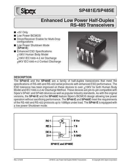
■+5V Only■Low Power BiCMOS■Driver/Receiver Enable for Multi-Drop configurations■Low Power Shutdown Mode (SP481E )■Enhanced ESD Specifications:DESCRIPTIONThe SP481E and the SP485E are a family of half-duplex transceivers that meet the specifications of RS-485 and RS-422 serial protocols with enhanced ESD performance. The ESD tolerance has been improved on these devices to over +15KV for both Human Body Model and IEC1000-4-2 Air Discharge Method. These devices are pin-to-pin compatible with Sipex's SP481 and SP485 devices as well as popular industry standards. As with the original versions, the SP481E and the SP485E feature Sipex's BiCMOS design allowing low power operation without sacrificing performance. The SP481E and SP485E meet the requirements of the RS-485 and RS-422 protocols up to 10Mbps under load. The SP481E is equipped with a low power Shutdown mode.+15KV Human Body Model+15KV IEC1000-4-2 Air Discharge +8KV IEC1000-4-2 Contact DischargeABSOLUTE MAXIMUM RATINGSThese are stress ratings only and functional operation of the device at these ratings or any other above those indicated in the operation sections of the specifications below is not implied. Exposure to absolute maximum rating conditions for extended periods of time may affect reliability.V CC ............................................................................................................+7V Input VoltagesLogic........................................................-0.3V to (V CC +0.5V)Drivers..................................................-0.3V to (V CC +0.5V)Receivers................................................................. ±15VSPECIFICATIONST MIN to T MAX and V CC = 5V ± 5% unless otherwise noted.PARAMETERSMIN.TYP.MAX.UNITS CONDITIONSSP481E/SP485E DRIVER DC CharacteristicsDifferential Output Voltage GND V CC Volts Unloaded; R = ∞; see Figure 1Differential Output Voltage 2V CC Volts with load; R = 50Ω; (RS-422);see Figure 1Differential Output Voltage 1.5V CC Volts with load; R = 27Ω; (RS-485);see Figure 1Change in Magnitude of Driver Differential Output Voltage for Complimentary States 0.2Volts R = 27Ω or R = 50Ω; see Figure 1Driver Common-Mode Output Voltage 3Volts R = 27Ω or R = 50Ω; see Figure 1Input High Voltage 2.0Volts Applies to DE, DI, RE Input Low Voltage 0.8Volts Applies to DE, DI, RE Input Current±10µA Applies to DE, DI, RE Driver Short-Circuit Current V OUT = HIGH ±250mA -7V ≤ V O ≤ +12V V OUT = LOW±250mA-7V ≤ V O ≤ +12VSP481E/SP485E DRIVER AC Characteristics Maximum Data Rate 10Mbps RE = 5V, DE = 5V; R DIFF = 54Ω,C L1 = C L2 = 100pFDriver Input to Output 203060ns t PLH ; R DIFF = 54Ω, C L1 = C L2 = 100pF;see Figures 3 and 5Driver Input to Output 203080ns t PLH ; R DIFF = 54Ω, C LI = C L2 = 100pF;(SP485EMN ONLY)See Figures 3 and 5Driver Input to Output 203060ns t PHL ; R DIFF = 54Ω, C L1 = C L2 = 100pF;see Figures 3 and 5Driver Input to Output 203080ns t PHL ; R DIFF = 54Ω, C L1 = C L2 = 100pF;(SP485EMN ONLY)see Figures 3 and 5Driver Skew510ns see Figures 3 and 5,t SKEW = | t DPLH - t DPHL |Driver Rise or Fall Time 31540ns From 10% to 90%; R DIFF = 54Ω,C L1 = C L2 = 100pF; s ee Figures 3 & 6Driver Enable to Output High 4070ns C L = 100pF; see Figures 4 & 6; S 2closedDriver Enable to Output Low 4070ns C L = 100pF; see Figures 4 & 6; S 1closedDriver Disable Time from Low 4070ns C L = 100pF; see Figures 4 & 6; S 1closedDriver Disable Time from High 4070nsC L = 100pF; see Figures 4 & 6; S 2closedOutput VoltagesLogic........................................................-0.3V to (V CC +0.5V)Drivers...................................................................... ±15V Receivers............................................-0.3V to (V CC +0.5V)Storage Temperature.......................................................-65˚C to +150˚C Power Dissipation per Package8-pin NSOIC (derate 6.60mW/o C above +70o C)...........................550mW 8-pin PDIP (derate 11.8mW/o C above +70o C)............................1000mW元器件交易网SPECIFICATIONS (continued)T MIN to T MAX and V CC = 5V ± 5% unless otherwise noted.PARAMETERS MIN.TYP.MAX.UNITS CONDITIONSSP481E/SP485E RECEIVER DC CharacteristicsDifferential Input Threshold -0.2+0.2Volts -7V ≤ V CM ≤ +12V Differential Input Threshold -0.4+0.4Volts -7V ≤ V CM ≤ +12V (SP485EMN ONLY)Input Hysteresis 20mV V CM = 0VOutput Voltage High 3.5Volts I O = -4mA, V ID = +200mV Output Voltage Low0.4Volts I O = +4mA, V ID = -200mVThree-State (High Impedance)Output Current ±1µA 0.4V ≤ V O ≤ 2.4V; RE = 5V Input Resistance 1215k Ω-7V ≤ V CM ≤ +12VInput Current (A, B); V IN = 12V +1.0mA DE = 0V, V CC = 0V or 5.25V, V IN = 12V Input Current (A, B); V IN = -7V -0.8mA DE = 0V, V CC = 0V or 5.25V, V IN = -7V Short-Circuit Current 795mA0V ≤ V O ≤ V CCSP481E/SP485E RECEIVER AC Characteristics Maximum Data Rate 10Mbps RE = 0V, DE = 0V Receiver Input to Output 2045100ns t PLH ; R DIFF = 54Ω,C L1 = C L2 = 100pF; Figures 3 & 7Receiver Input to Output 2045100ns t PHL ; R DIFF = 54Ω,C L1 = C L2 = 100pF; Figures 3 & 7Diff. Receiver Skew It PLH -t PHL I 13nsR DIFF = 54Ω; C L1 = C L2 = 100pF;Figures 3 & 7Receiver Enable to Output Low4570ns C RL = 15pF; Figures 2 & 8; S 1 closed Receiver Enable to Output High4570ns C RL = 15pF; Figures 2 & 8; S 2 closed Receiver Disable from Low 4570ns C RL = 15pF; Figures 2 & 8; S 1 closed Receiver Disable from High 4570nsC RL = 15pF; Figures 2 & 8; S 2 closed SP481EShutdown Timing Time to Shutdown 50200600ns RE = 5V, DE = 0VDriver Enable from Shutdown to Output High40100ns C L = 100pF; See Figures 4 & 6; S 2 closed Driver Enable from Shutdown to Output Low40100ns C L = 100pF; See Figures 4 & 6; S 1 closed Receiver Enable from Shutdown to Output High 3001000ns C L = 15pF; See Figures 2 & 8; S 2 closed Receiver Enable from Shutdown to Output Low 3001000ns C L = 15pF; See Figures 2 & 8; S 1 closedPOWER REQUIREMENTS Supply Voltage +4.75+5.25VoltsSupply Current SP481E/485E No Load900µA RE, DI = 0V or V CC ; DE = V CC 600µA RE = 0V, DI = 0V or 5V; DE = 0V SP481EShutdown Mode10µADE = 0V, RE=V CCENVIRONMENTAL AND MECHANICAL Operating Temperature Commercial (_C_)0+70°C Industrial (_E_)-40+85°C (_M_)-40+125°C Storage Temperature -65+150°CPackagePlastic DIP (_P) NSOIC (_N)元器件交易网PIN FUNCTIONPin 1 – RO – Receiver Output.Pin 2 – RE – Receiver Output Enable Active LOW.Pin 3 – DE – Driver Output Enable Active HIGH.Pin 4 – DI – Driver Input.Pin 5 – GND – Ground Connection.Pin 6 – A – Driver Output/Receiver Input Non-inverting.Pin 7 – B – Driver Output/Receiver Input Inverting.Pin 8 – Vcc – Positive Supply 4.75V<Vcc< 5.25V.Figure 5. Driver Propagation DelaysFigure 3. RS-485 Driver/Receiver Timing Test CircuitFigure 4. RS-485 Driver Timing Test Load #2 CircuitINPUTS OUTPUTSLINERE DE DI CONDITION B A X11No Fault01 X10No Fault10 X0X X Z Z X1X Fault Z ZINPUTS OUTPUTS RE DE A - B R00 +0.2V100 -0.2V000Inputs Open110X ZTable 1. Transmit Function Truth TableTable 2. Receive Function Truth TableFigure 8. Receiver Enable and Disable Times元器件交易网ReceiversThe SP481E and SP485E receivers have differ-ential inputs with an input sensitivity as low as ±200mV. Input impedance of the receivers is typically 15k Ω (12k Ω minimum). A wide com-mon mode range of -7V to +12V allows for large ground potential differences between systems.The receivers of the SP481E and SP485E have a tri-state enable control pin. A logic LOW on RE (pin 2) will enable the receiver, a logic HIGH on RE (pin 2) will disable the receiver.The receiver for the SP481E and SP485E will operate up to at least 10Mbps. The receiver for each of the two devices is equipped with the fail-safe feature. Fail-safe guarantees that the receiver output will be in a HIGH state when the input is left unconnected.Shutdown Mode SP481EThe SP481E is equipped with a Shutdown mode.To enable the Shutdown state, both the driver and receiver must be disabled simultaneously.A logic LOW on DE (pin 3) and a logic HIGH on RE (pin 2) will put the SP481E into Shutdown mode. In Shutdown, supply current will drop to typically 1µA.ESD TOLERANCEThe SP481E Family incorporates ruggedized ESD cells on all driver output and receiver input pins. The ESD structure is improved over our previous family for more rugged applications and environments sensitive to electro-static dis-charges and associated transients. The improved ESD tolerance is at least ±15kV without damage nor latch-up.There are different methods of ESD testing applied:a) MIL-STD-883, Method 3015.7b) IEC1000-4-2 Air-Discharge c) IEC1000-4-2 Direct ContactDESCRIPTIONThe SP481E and SP485E are half-duplex differ-ential transceivers that meet the requirements of RS-485 and RS-422. Fabricated with a Sipex proprietary BiCMOS process, all three products require a fraction of the power of older bipolar designs.The RS-485 standard is ideal for multi-drop applications and for long-distance interfaces.RS-485 allows up to 32 drivers and 32 receivers to be connected to a data bus, making it an ideal choice for multi-drop applications. Since the cabling can be as long as 4,000 feet, RS-485transceivers are equipped with a wide (-7V to +12V) common mode range to accommodate ground potential differences. Because RS-485 is a differential interface, data is virtually immune to noise in the transmission line.DriversThe driver outputs of the SP481E and SP485E are differential outputs meeting the RS-485 and RS-422 standards. The typical voltage output swing with no load will be 0 Volts to +5 Volts.With worst case loading of 54Ω across the differ-ential outputs, the drivers can maintain greater than 1.5V voltage levels. The drivers of the SP481E , and SP485E have an enable control line which is active HIGH. A logic HIGH on DE (pin 3) will enable the differential driver outputs.A logic LOW on DE (pin 3) will tri-state the driver outputs.The transmitters of the SP481E and SP485E will operate up to at least 10Mbps.元器件交易网The Human Body Model has been the generally accepted ESD testing method for semiconductors. This method is also specified in MIL-STD-883, Method 3015.7 for ESD testing. The premise of this ESD test is to simulate the human body’s potential to store electro-static energy and discharge it to an integrated circuit. The simulation is performed by using a test model as shown in Figure 7. This method will test the IC’s capability to withstand an ESD transient during normal handling such as in manufacturing areas where the ICs tend to be handled frequently. The IEC-1000-4-2, formerly IEC801-2, is generally used for testing ESD on equipment and systems. For system manufacturers, they must guarantee a certain amount of ESD protection since the system itself is exposed to the outside environment and human presence. The premise with IEC1000-4-2 is that the system is required to withstand an amount of static electricity when ESD is applied to points and surfaces of the equipment that are accessible to personnel during normal usage. The transceiver IC receives most of the ESD current when the ESD source is applied to the connector pins. The test circuit for IEC1000-4-2 is shown on Figure 8. There are two methods within IEC1000-4-2, the Air Discharge method and the Contact Discharge method.Figure 7. ESD Test Circuit for Human Body ModelFigure 8. ESD Test Circuit for IEC1000-4-2元器件交易网With the Air Discharge Method, an ESD voltage is applied to the equipment under test (EUT) through air. This simulates an electrically charged person ready to connect a cable onto the rear of the system only to find an unpleasant zap just before the person touches the back panel. The high energy potential on the person discharges through an arcing path to the rear panel of the system before he or she even touches the system. This energy, whether discharged directly or through air, is predominantly a function of the discharge current rather than the discharge voltage. Variables with an air discharge such as approach speed of the object carrying the ESD potential to the system and humidity will tend to change the discharge current. For example, the rise time of the discharge current varies with the approach speed.The Contact Discharge Method applies the ESD current directly to the EUT. This method was devised to reduce the unpredictability of the ESD arc. The discharge current rise time is constant since the energy is directly transferred without the air-gap arc. In situations such as hand held systems, the ESD charge can be directly discharged to the equipment from a person already holding the equipment. The current is transferred on to the keypad or the serial port of the equipment directly and then travels through the PCB and finally to the IC.The circuit model in Figures 7 and 8 represent the typical ESD testing circuit used for all three methods. The C S is initially charged with the DC power supply when the first switch (SW1) is on. Now that the capacitor is charged, the second switch (SW2) is on while SW1 switches off. The voltage stored in the capacitor is then applied through R S, the current limiting resistor, onto the device under test (DUT). In ESD tests, the SW2 switch is pulsed so that the device under test receives a duration of voltage.For the Human Body Model, the current limiting resistor (RS) and the source capacitor (CS) are 1.5kΩ an 100pF, respectively. For IEC-1000-4-2, the current limiting resistor (RS) and the source capacitor (CS) are 330Ω an 150pF, respectively.The higher CSvalue and lower RSvalue in the IEC1000-4-2 model are more stringent than the Human Body Model. The larger storage capacitor injects a higher voltage to the test point when SW2 is switched on. The lower current limiting resistor increases the current charge onto the test point.Figure 9. ESD Test Waveform for IEC1000-4-2t=0ns t=30ns0A15A30At ➙i➙元器件交易网元器件交易网ORDERING INFORMATIONModel Temperature Range PackageSP481ECN.......................................................0˚C to +70˚C...............................................8-pin Narrow SOICSP481ECP........................................................0˚C to +70˚C...................................................8-pin Plastic DIPSP481EEN.......................................................-40˚C to +85˚C.............................................8-pin Narrow SOICSP481EEP......................................................-40˚C to +85˚C.................................................8-pin Plastic DIPSP485ECN.......................................................0˚C to +70˚C...............................................8-pin Narrow SOICSP485ECP........................................................0˚C to +70˚C...................................................8-pin Plastic DIPSP485EEN......................................................-40˚C to +85˚C.............................................8-pin Narrow SOICSP485EEP......................................................-40˚C to +85˚C.................................................8-pin Plastic DIPSP485EMN....................................................-40˚C to +125˚C............................................8-pin Narrow SOICPlease consult the factory for pricing and availability on a Tape-On-Reel option.CorporationSIGNAL PROCESSING EXCELLENCESipex CorporationHeadquarters andSales Office233 South Hillview DriveMilpitas, CA 95035TEL: (408) 934-7500FAX: (408) 935-7600Sales Office22 Linnell CircleBillerica, MA 01821TEL: (978) 667-8700FAX: (978) 670-9001e-mail: sales@Sipex Corporation reserves the right to make changes to any products described herein. Sipex does not assume any liability arising out of theapplication or use of any product or circuit described herein; neither does it convey any license under its patent rights nor the rights of others.Rev. 5/16/03SP481E Low Power Half-Duplex RS485 Transceivers© Copyright 2003 Sipex Corporation11。
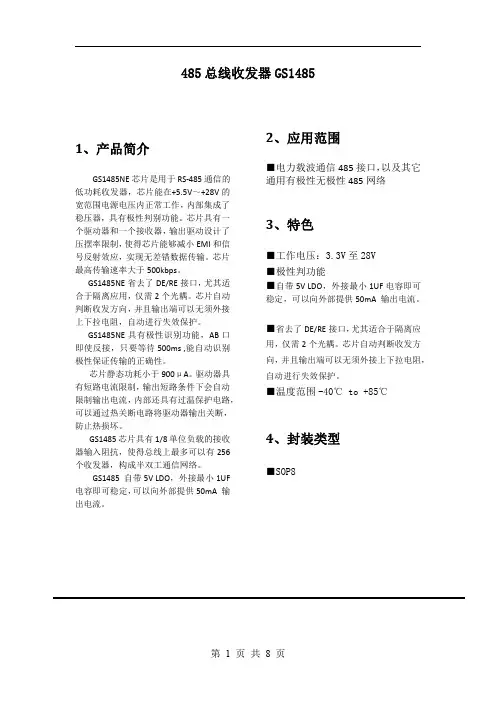
常用485芯片
常用的485芯片是一种用于工业自动化领域的通信芯片,它采用RS-485标准通信协议,能够提供可靠的长距离或多节点通信解决方案。
以下是一些常见的485芯片及其特点:
1. MAX485:MAX485是一款经典的485转换芯片,它具有低功耗、高速传输、抗干扰能力强等特点。
它可以支持半双工通信模式,并且能够实现单个总线上多个节点的通信。
MAX485芯片广泛应用于工业自动化、电力系统、安防监控等领域。
2. SN75176:SN75176是另一种常用的485转换芯片,它具有低功耗、高速传输、抗干扰能力强等特点。
与MAX485相比,SN75176芯片的驱动能力更强,能够实现更长距离的传输。
SN75176芯片广泛应用于电力系统、通信设备、仪器仪表等领域。
3. ADM485:ADM485是ADI公司生产的一款485转换芯片,它具有低功耗、高速传输、抗干扰能力强等特点。
ADM485芯片采用了双差分驱动模式,能够实现更高的传输速率和更好的信号质量。
ADM485芯片广泛应用于工业自动化、仪器仪表、交通系统等领域。
4. LTC485:LTC485是LT公司生产的一款高性能485转换芯片,它具有低功耗、高速传输、抗干扰能力强等特点。
LTC485芯片采用了
差分线路保护技术,能够有效抵抗电磁干扰和电气冲击。
LTC485芯片广泛应用于工业自动化、电力系统、通信设备等领域。
总的来说,485芯片是工业自动化领域中常用的通信芯片,它具有可靠的长距离传输能力和多节点通信能力。
选择适合的485芯片可以提高系统的稳定性和可靠性,实现更高效的数据通信。
一、RS485基本知识RS-485接口芯片已广泛应用于工业控制、仪器、仪表、多媒体网络、机电一体化产品等诸多领域。
可用于RS-485接口的芯片种类也越来越多。
如何在种类繁多的接口芯片中找到最合适的芯片,是摆在每一个使用者面前的一个问题。
RS-485接口在不同的使用场合,对芯片的要求和使用方法也有所不同。
使用者在芯片的选型和电路的设计上应考虑哪些因素,由于某些芯片的固有特性,通信中有些故障甚至还需要在软件上作相应调整,如此等等。
希望本文对解决RS-485接口的某些常见问题有所帮助。
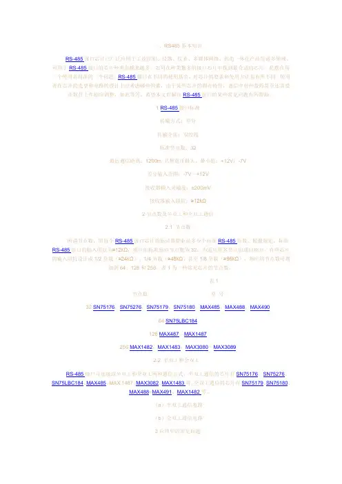
1 RS-485接口标准传输方式:差分传输介质:双绞线标准节点数:32最远通信距离:1200m 共模电压最大、最小值:+12V;-7V差分输入范围:-7V~+12V接收器输入灵敏度:±200mV接收器输入阻抗:≥12kΩ2 节点数及半双工和全双工通信2.1 节点数所谓节点数,即每个RS-485接口芯片的驱动器能驱动多少个标准RS-485负载。
根据规定,标准RS-485接口的输入阻抗为≥12kΩ,相应的标准驱动节点数为32。
为适应更多节点的通信场合,有些芯片的输入阻抗设计成1/2负载(≥24kΩ)、1/4负载(≥48kΩ)甚至1/8负载(≥96kΩ),相应的节点数可增加到64、128和256。
表1为一些常见芯片的节点数。
表1节点数型号32 SN75176,SN75276,SN75179,SN75180,MAX485,MAX488,MAX49064 SN75LBC184128 MAX487,MAX1487256 MAX1482,MAX1483,MAX3080~MAX30892.2 半双工和全双工RS-485接口可连接成半双工和全双工两种通信方式。
半双工通信的芯片有SN75176、SN75276、SN75LBC184、MAX485、MAX 1487、MAX3082、MAX1483等;全双工通信的芯片有SN75179、SN75180、MAX488~MAX491、MAX1482等。
信号和电源隔离RS-485现场总线的高速或低功耗解决方案简介ADI公司的iCoupler®数字隔离器和RS-485收发器产品系列解决了工业应用中的两大需求:更高的数据速率和更低功耗的工作模式。
对于高性能电机控制编码器应用而言,通常需要更高的数据速率、更小的RS-485收发器封装和IEC 61000-4-2 ESD保护。
ADM3065E/ADM3066E50 Mbps收发器采用节省空间的10引脚LFCSP 封装,可提供±12 kV(接触)和±12 kV(空气)的IEC61000-4-2 ESD 保护功能,为EnDat编码器提供了一套可靠的解决方案(请参考AN-1397应用笔记了解更多信息)。
此外,在ADM3065E/ADM3066E 中添加高速稳定的信号和功率隔离可以通过isoPower®ADuM6401或isoPowerADuM6000及iCouplerADuM241D来实现,如本应用笔记中所述。
在电池供电系统、井下应用(例如,采矿)以及在4 mA至20 mA 环路中工作的过程控制系统中,往往对低功耗工作模式具有较高需求。
ADI公司生产的微功耗数字隔离器ADuM1441在关断模式下的静态功耗低于23 μA。
ADM34833.3 V、250 kbps RS-485收发器的静态功耗极低,关断模式下通常仅2 nA。
图1所示为适合井下应用稳定可靠的低功耗隔离式RS-485解决方案。
ADM3483和ADuM1441共用可提供一条通往远程地下测量节点的可靠低功耗链路。
系统接口卡包括ARM®Cortex®微控制器单元(MCU)、ADuCM3027和集成模拟前端(AFE)AD7124-4,用于远程温度和压力测量。
系统接口卡的固件更新通过远距离RS-485电缆提供,更新后能够在最长1 km的远距离内实现低数据速率传输(例如,9.6 kbps)。
图1.适合井下应用稳定可靠的低功耗隔离式RS-485解决方案隔离式高速RS-485利用iCoupler和isoPower技术,可以向ADM3065E中增添兼具加强绝缘和5 kV rms瞬态耐受电压的电流隔离。
特性阻抗是指当电缆无限长时该电缆所具有的阻抗,是阻止电流通过导体的一种电阻名称,它不是常规意义上的直流电阻。
一条电缆的特性阻抗是由电缆的电导率、电容以及阻值组合后的综合特性。
假设一根均匀电缆无限延伸,在发射端的在某一频率下的阻抗称为“特性阻抗”(Characteristic Impedance)。
这些参数是由诸如导体尺寸、导体间的距离以及电缆绝缘材料特性等物理参数决定的。
测量特性阻抗时,可在电缆的另一端用特性阻抗的等值电阻终接,其测量结果会跟输入信号的频率有关。
特性阻抗的测量单位为欧姆。
在高频段频率不断提高时,特性阻抗会渐近于固定值。
例如同轴线将会是50或75欧姆;而常用非屏蔽双绞线的特性阻抗为100欧姆,屏蔽双绞线的特性阻抗为150欧姆。
正常的物理运行依靠整个系统电缆与连接器件具有的恒定的特性阻抗。
特性阻抗通常可以由电缆的连接和端结而造成轻微的改变。
电缆的硬转弯或纽结也会改变电缆的特性阻抗。
在不连续较轻的情况下,由于反射的信号微弱而且又经过电缆的衰减,所以对网络来说仍然能运行。
大的阻抗不连续将会干扰数据传输。
这类的不连续是由不良的电气连接、不正确的电缆端结、不匹配的电缆和不匹配的连接器的使用以及电缆中双绞电缆对的绞结方式错误而造成的。
在综合布线系统中,有很多忌讳,如:双绞线如果断开,是不可以直接直接连接在一起的,拉力不可过大,对于非屏蔽线缆弯曲半径至少为4倍的线缆外径,千万不要混用特性阻抗不同的电缆等等,这些都会导致特性阻抗的改变,在验收测试中,就表现为回波损耗测试参数较低。
本篇文章来自<A href=''>IDC专家网</a> 原文链接:/articles/1215484971056/20081121/1215945565594_1.html提高485总线的可靠性摘要:就485总线应用中易出现的问题,分析了产生的原因并给出解决问题的软硬件方案和措施。
关键词:RS-485总线、串行异步通信--------------------------------------------------------------------------------1 问题的提出在应用系统中,RS-485半双工异步通信总线是被各个研发机构广泛使用的数据通信总线,它往往应用在集中控制枢纽与分散控制单元之间。
KODENSHI AUK专注于硅半导体,化合物半导体,光传感器领域33年,集团根据不同的哑群分别独立设立公司,这些公司已发展成为各自领域的专业公司,向全球提供国际水准的核心器件,广泛应用于人类未来泛在信息社会重要铸成部分的家用电器,工业设备,IT 产品等尖端数码技术产品。
KODENSHI AUK集团1972年创始于日本京都,行业内亦称为光电子集团。
经过40多年的发展,集团在全球拥有多个研发、生产基地及全球化销售网络,成员遍及中国、日本、韩国、美国、新加坡等多个国家,如今已成为世界一流的半导体公司。
为了致力于中国市场,服务中国客户,集团早在1992年即进入中国,先后在沈阳、大连、深圳、上海等地投资创建沈阳中光电子有限公司、可天士半导体(沈阳)有限公司等多家企业。
并在北京、上海、深圳、青岛、合肥、成都、厦门、西安、香港、台湾等地设有销售公司及办事处。
可天士半导体(沈阳)有限公司作为KODENSHI AUK集团在华拓展中国市场的的主导品牌,继承了集团产品的高品质、高信赖性的基因,用高品质产品和一流的技术服务于大中国区客户。
拥有从Wafer制作、IC设计到产品封装,直至模块开发,OEM/ODM等业务的专业能力。
主要大中国区域的新产品开发、市场开拓、渠道管理、技术支持、售后服务等相关业务。
公司自成立以来,始终坚持以快速设计开发能力和高品质保证提供给客户优质的产品,荟萃业界精英,将国外先进的技术、管理方法及企业经验与国内企业的具体实际相结合,使企业在激烈的市场竞争中始终保持竞争力,实现企业快速、稳定地发展。
公司先后通过了TS16949、ISO9001、ISO14001、OHSAS18001等认证。
沈阳中光电子有限公司成立于1992年8月,注册资本17,452,140美元。
公司位于沈阳经济技术开发区,现有员工2000多名,主要从事光电二极管、光电三极管、光电开关、光电编码器、纸张感应器,光电耦合器等光电器件的开发、生产与销售。
ZZ-ST-485-RS485型温振传感器使用说明书(V1.2)济南智泽贸易有限公司目录1.产品简介 (3)1.1.产品概述 (3)1.2.技术参数 (3)1.3.应用领域 (3)2.产品安装 (4)3.Modbus通讯 (4)3.1.读保持寄存器功能码0x03 (4)3.2.预置单个寄存器功能码0x06 (5)3.3.寄存器列表 (6)4.传感器尺寸 (6)5.联系方式 (7)6.免责声明 (7)7.质保与售后 (7)8.修订记录 (7)1.产品简介1.1.产品概述485型温振传感器是选用高性能的MEMS芯片,采用嵌入式技术、温度传感技术、振动传感技术开发生产的一款高性能、抗干扰和复合型振动传感器。
1.2.技术参数主要指标技术参数规格型号ZZ-ST-485温振传感器芯片技术MEMS,测点全、精度高振动测量范围0-50mm/s振动测量精度±1.5%F.S.mm/s振动测量方向X轴、Y轴、Z轴频率范围10~1600Hz温度测量范围-40~150℃温度测量精度±0.5℃信号输出RS485检测周期实时,主站查询,从机应答供电方式外部供电供电电压DC12~24V防护等级IP67接线方式红、黑为电源的正、负极,黄、绿为485A+、485B-外形尺寸Φ24mm×60mm(筒径×高度)27mm(底部螺母对边)M8×10mm(螺纹)1.3.应用领域智能温度振动传感器广泛应用于煤矿、化工、冶金、发电等行业的电机、减速机风机、发电机、空压机、离心机、水泵等旋转设备温度和三轴振动的在线测量。
2.产品安装(1)开箱检查从包装箱中取出传感器,检查传感器外观是否良好、引线是否完好。
(2)读取和修改传感器地址。
设备出厂时的默认地址均为“1”。
使用串口助手或专用的配置软件可以修改设备地址。
设备地址:1-240。
(3)传感器安装。
磁吸的:将传感器直接吸附在设备的振动测量位置。
螺栓的:将传感器底部的∮8×10mm的螺栓拧紧在设备的振动测量位置。
485芯片选型485总线通讯是一种常见的工业自动化通信技术,其中485芯片是实现485总线通讯的关键组成部分之一。
本文将从不同厂家的485芯片选型方面进行探讨,并对几款常见的485芯片进行介绍。
首先,选择485芯片需要考虑的因素包括通信速率、工作电压、功耗、价格和可靠性等。
根据具体的应用需求,可以选择适合的芯片型号。
在通信速率方面,一般的485芯片支持的速率范围为300bps到10Mbps,可以根据具体的通信要求进行选择。
例如,对于速率要求较高的应用场景,可以选择支持较高速率的芯片,如TI的SN65HVD78和Maxim的MAX485。
工作电压是另一个重要因素,它一般决定了485芯片的适用范围。
对于工业自动化领域,常见的工作电压为5V和3.3V。
因此,在选择485芯片时,需要确保其工作电压符合系统的要求。
功耗是另一个需要考虑的因素,特别是对于低功耗应用来说。
一般来说,功耗较低的485芯片能够延长电池寿命,降低能耗。
一些低功耗的芯片如TI的SN65HVD3082和ON的SP3082。
价格也是选择485芯片时需要考虑的因素之一。
不同厂家的485芯片价格有所差异,同时,价格还受到规格和性能的影响。
因此,在选择485芯片时,需要综合考虑成本和性能。
另外,可靠性也是485芯片选型时需要考虑的重要因素之一。
可靠性包括芯片的抗干扰能力、抗ESD能力等。
在工业自动化领域,环境复杂,抗干扰能力要求较高,因此,在选择485芯片时,需要考虑其抗干扰能力。
下面介绍几款常见的485芯片:1. TI的SN65HVD78:这款芯片是一款低功耗485收发器,工作电压范围为3.3V到5V,支持速率为50kbps到40Mbps,具有较好的抗ESD能力和抗干扰能力。
2. Maxim的MAX485:这款芯片是一款经典的485收发器,工作电压范围为4.5V到5.5V,支持速率为2.5Mbps,价格较为实惠。
3. ON的SP3082:这款芯片是一款低功耗的485收发器,工作电压范围为3V到5.5V,支持速率为250kbps,具有较好的抗干扰能力和抗ESD能力。
rs485芯片RS-485芯片是一种常见的通信接口芯片,它被广泛应用于工业自动化、仪器仪表和数据采集系统等领域,下面将对RS-485芯片进行详细解析。
RS-485是一种串行通信接口标准,它定义了一套物理层和传输层规范,用于在多点传输线上进行点对点或多点传输。
与RS-232接口相比,RS-485接口具有更高的传输速率、更远的传输距离和更强的抗干扰能力。
因此,在需要长距离传输且抗干扰能力要求较高的场景中,RS-485接口更为常见。
RS-485芯片一般由收发器和线路驱动器两部分组成。
收发器负责将电平转换为RS-485标准的差分信号,以便进行传输。
线路驱动器负责提供足够的驱动能力,以确保信号能够在传输线上准确地传输。
RS-485芯片通常支持半双工或全双工通信模式,并且可以通过设置控制引脚来切换通信模式。
RS-485芯片通常具有以下特点和功能:1. 高速传输:RS-485接口具有较高的传输速率,通常可以达到10Mbps以上。
这使得RS-485芯片非常适合于需要高速数据传输的应用,例如实时数据采集和远程控制系统。
2. 长传输距离:RS-485接口能够在较长的传输线上进行通信,通常可以覆盖数百米的距离。
这使得RS-485芯片非常适合于远程监控和数据采集系统。
3. 多点传输:RS-485接口支持多点传输,可以在同一传输线上连接多个设备。
这使得RS-485芯片非常适合于工业自动化和仪器仪表等需要多个设备之间进行通信的场景。
4. 抗干扰能力强:RS-485接口的差分传输方式使其具有较强的抗干扰能力,能够在工业环境中稳定可靠地传输信号。
这使得RS-485芯片非常适合于电磁干扰较大的工业现场。
5. 低功耗:RS-485芯片通常采用低功耗设计,以降低功耗和热量产生。
这使得RS-485芯片非常适合于嵌入式系统和便携式设备。
总之,RS-485芯片作为一种常见的通信接口芯片,具有高速传输、长传输距离、多点传输和抗干扰能力强等特点,被广泛应用于工业自动化、仪器仪表和数据采集系统等领域。
February 2009Rev 141/18ST485EBST485EC - ST485EX±15 kV ESD protected, low powerRS-485/RS-422 transceiverFeatures■Low quiescent current: 300 µA■Designed for RS-485 interface application ■- 7 V to 12 V common mode input voltage range ■Driver maintains high impedance in 3-state or with the power OFF■70 mV typical input hysteresis ■30 ns propagation delay, 5 ns skew ■Operates from a single 5 V supply ■Current limiting and thermal shutdown for driver overload protection■ESD protection:–± 15 kV (HBM)–± 8 kV (IEC-1000-4-2 contact discharge)■Allows up to 256 transceivers on the busDescriptionThe ST485E is a low power transceiver for RS-485 and RS-422 communication. Each driver output and receiver input is protected against ± 15 kV electrostatic discharge (HBM) (ESD) shocks, without latch-up. These parts contain one driver and one receiver in half duplex configuration.This transceiver draws 300 µA (typ.) of supply current when unloaded or fully loaded with disabled drivers.It operates from a single 5 V supply.Driver is short-circuit current limited and isprotected against excessive power dissipation by thermal shutdown circuitry that place the driver outputs into a high-impedance state.The ST485E is designed for bi-directional data communications on multipoint bus transmission lines (half-duplex applications).Table 1.Device summaryOrder codes Temperaturerange Package PackagingST485EBD - 40 to 85 °C SO-8 (tube)100 parts per tube / 20 tube per boxST485ECDR 0 to 70 °C SO-8 (tape and reel)2500 parts per reel ST485EBDR - 40 to 85 °C SO-8 (tape and reel)2500 parts per reel ST485EXDR- 55 to 125 °CSO-8 (tape and reel)2500 parts per reelContents ST485EB - ST485EC - ST485EX Contents1Pin configuration . . . . . . . . . . . . . . . . . . . . . . . . . . . . . . . . . . . . . . . . . . . 3 2Truth tables . . . . . . . . . . . . . . . . . . . . . . . . . . . . . . . . . . . . . . . . . . . . . . . . 4 3Maximum ratings . . . . . . . . . . . . . . . . . . . . . . . . . . . . . . . . . . . . . . . . . . . 5 4Electrical characteristics . . . . . . . . . . . . . . . . . . . . . . . . . . . . . . . . . . . . . 6 5Test circuit and typical characteristics . . . . . . . . . . . . . . . . . . . . . . . . . . 9 6Package mechanical data . . . . . . . . . . . . . . . . . . . . . . . . . . . . . . . . . . . . 14 7Revision history . . . . . . . . . . . . . . . . . . . . . . . . . . . . . . . . . . . . . . . . . . . 172/18ST485EB - ST485EC - ST485EX Pin configuration3/181 Pin configurationTable 2.Pin descriptionPin n° Symbol Name and function1RO Receiver output 2RE Receiver output enable 3DE Driver output enable 4DI Driver input 5GND Ground6A Non-inverting receiver input and non-inverting driver output 7B Inverting receiver input and inverting driver output 8V CCSupply voltageTruth tables ST485EB - ST485EC - ST485EX4/182 Truth tablesNote:X = Don’t care; Z = High impedance Note:X = Don’t care; Z = High impedanceTable 3.Truth table (driver)InputsOutputsRE DE DI B A X H H L H X H L H L XLXZZTable 4.Truth table (receiver)InputsOutputs RE DE A-BRO L L ≥ +0.2V H L L ≤ -0.2VL L L Inputs openH HLXZST485EB - ST485EC - ST485EX Maximum ratings 3 Maximum ratingsTable 5.Absolute maximum ratingsSymbol Parameter Value Unit V CC Supply voltage7V V I Control input voltage (RE, DE)-0.5 to (V CC + 0.5)V V DI Driver input voltage (DI)-0.5 to (V CC + 0.5)V V DO Driver output voltage (A, B)± 14V V RI Receiver input voltage (A, B)± 14V V RO Receiver output voltage (RO)-0.5 to (V CC + 0.5)VNote:Absolute maximum ratings are those values beyond which damage to the device may occur.Functional operation under these is not implied.5/18Electrical characteristics ST485EB - ST485EC - ST485EX6/184 Electrical characteristicsV CC = 5 V ± 5 %, T A = T MIN to T MAX , unless otherwise specified. Typical values are referredto T A = 25 °CTable 6.ESD performance: transmitter outputs, receiver inputsSymbol ParameterTest conditions Min.Typ.Max.Unit ESD ESD protection voltage Human body model ±15kV ESDESD protection voltageIEC-1000-4-2±8kVTable 7.DC electrical characteristicsSymbol ParameterTest conditions (1)Min.Typ.Max.Unit V OD1Differential driver output (no load)5V V OD2Differential driver output (with load)R L = 27 Ω (RS-485) (Figure 2)R L = 50 Ω (RS-422) (Figure 2.) 1.555V VΔV ODChange in magnitude of driver differential output voltage for complementary output statesR L = 27 Ω or 50 Ω (Figure 2)0.2VV OCDriver common-mode outputvoltageR L = 27 Ω or 50 Ω (Figure 2)3VΔV OC Change in magnitude of driver common-mode outputvoltage for complementary output states R L = 27 Ω or 50 Ω (Figure 2)0.2VV IH Input high voltage RE, DE, DI 2.0VV IL Input low voltage RE, DE, DI 0.8V I IN1Input current RE, DE, DI± 2µA I IN2Input current (A, B)V CM = 0 V or 5.25 V , V DE = 0 V V IN = 12 V V IN = -7 V 1-0.8mA mA V TH Receiver differential threshold voltage V CM = -7 to 12 V -0.20.2V ΔV TH Receiver input hysteresisV CM = 0 V70mV V OH Receiver output high voltage I O = -4 mA, V ID = 200 mV 3.5VV OL Receiver output low voltage I O = 4 mA, V ID = -200 mV 0.4V I OZR 3-State (high impedance) output current at receiver V O = 0.4 to 2.4 V ± 1µA R IN Receiver input resistance V CM = -7 to 12 V 96k ΩI CCNo load supply current(2)V RE = 0V or V CC V DE = V CC V DE = 0 V400300900500µA µAST485EB - ST485EC - ST485EX Electrical characteristics7/18V CC = 5 V ± 5 %, T A = T MIN to T MAX , unless otherwise specified. Typical values are referred to T A = 25 °CI OSD1Driver short-circuit current, V O =HighV O = -7 to 12 V (3)35250mA I OSD2Driver short-circuit current, V O =LowV O = -7 to 12 V (3)35250mA I OSRReceiver short-circuit current V O = 0 V to V CC795mA1.All currents into device pins are positive; all out of device pins are negative; all voltages are referenced to device groundunless specified.2.Supply current specification is valid for loaded transmitters when V DE = 0 V 3.Applies to peak current. See typical Operating Characteristics.Table 7.DC electrical characteristics (continued)Symbol ParameterTest conditions (1)Min.Typ.Max.Unit Table 8.Driver switching characteristicsSymbol ParameterTest conditions (1)Min.Typ.Max.Unit t PLH t PHL Propagation delay input to output R DIFF = 54 Ω, C L1 = C L2 = 100 pF (See Figure 4 and Figure 6) 2545ns t SK Output skew to output R DIFF = 54 Ω, C L1 = C L2 = 100 pF(See Figure 4 and Figure 6)25ns t TLH t THL Rise or fall time R DIFF = 54 Ω, C L1 = C L2 = 100 pF (See Figure 4 and Figure 6) 1540ns t PZH Output enable time C L = 100 pF , S2 = Closed (See Figure 5 and Figure 7)3550ns t PZL Output enable time C L = 100 pF , S1 = Closed (See Figure 5 and Figure 7)2540ns t PLZ Output disable time C L = 15 pF , S1 = Closed (See Figure 5 and Figure 7)2540ns t PHZOutput disable timeC L = 15 pF , S2 = Closed (See Figure 5 and Figure 7)3550ns1.All currents into device pins are positive; all out of device pins are negative; all voltages are referenced to device groundunless specified.Electrical characteristics ST485EB - ST485EC - ST485EX8/18V CC = 5 V ± 5%, T A = T MIN to T MAX, unless otherwise specified. Typical values are referred to T A = 25 °CTable 9.Receiver switching characteristicsSymbol Parameter Test conditions (1)Min.Typ.Max.Unitt PLH t PHL Propagation delay input tooutputR DIFF = 54 Ω, C L1 = C L2 = 100 pF(See Figure4 and Figure8)110130nst SKD Differential receiver skew R DIFF = 54 Ω, C L1 = C L2 = 100 pF(See Figure4 and Figure8)510nst PZH Output enable time C RL = 15 pF, S1 = Closed(See Figure2 and Figure9)1135nst PZL Output enable time C RL = 15 pF, S2 = Closed(See Figure2 and Figure9)1335nst PLZ Output disable time C RL = 15 pF, S1 = Closed(See Figure2 and Figure9)1335nst PHZ Output disable time C RL = 15 pF, S2 = Closed(See Figure2 and Figure9)1135nsf MAX Maximum data rate5Mbps1.All currents into device pins are positive; all out of device pins are negative; all voltages are referenced to device groundunless specifiedST485EB - ST485EC - ST485EX Test circuit and typical characteristics 5 Test circuit and typical characteristics9/18Test circuit and typical characteristics ST485EB - ST485EC - ST485EX10/18ST485EB - ST485EC - ST485EX Test circuit and typical characteristicsTest circuit and typical characteristics ST485EB - ST485EC - ST485EX Figure 10.Receiver output current vs. output Figure 11.Receiver output current vs. outputFigure 12.Driver output current vs. output low Figure 13.Driver output current vs. outputFigure 14.Supply current vs. temperature Figure 15.Receiver high level output voltageST485EB - ST485EC - ST485EX Test circuit and typical characteristics Figure 16.Receiver low level output voltage Figure 17.Differential driver output voltage vs.Package mechanical data ST485EB - ST485EC - ST485EX 6 Package mechanical dataIn order to meet environmental requirements, ST offers these devices in different grades ofECOPACK® packages, depending on their level of environmental compliance. ECOPACK®specifications, grade definitions and product status are available at: . ECOPACKis an ST trademark.ST485EB - ST485EC - ST485EX Package mechanical dataPackage mechanical data ST485EB - ST485EC - ST485EXST485EB - ST485EC - ST485EX Revision historyhistory7 RevisionTable 10.Document revision historyDate Revision Changes21-Mar-20069Order codes has been updated and new template.05-Jun-200610Change value row 10 on the features and R IN in T able7.29-Jan-200711Typo mistake on page 1.29-Aug-200712Change value R IN min. on T able7.07-Feb-200813Modified: Table1 on page1.16-Feb-200914Modified: Note: on page 5.ST485EB - ST485EC - ST485EXPlease Read Carefully:Information in this document is provided solely in connection with ST products. STMicroelectronics NV and its subsidiaries (“ST”) reserve the right to make changes, corrections, modifications or improvements, to this document, and the products and services described herein at any time, without notice.All ST products are sold pursuant to ST’s terms and conditions of sale.Purchasers are solely responsible for the choice, selection and use of the ST products and services described herein, and ST assumes no liability whatsoever relating to the choice, selection or use of the ST products and services described herein.No license, express or implied, by estoppel or otherwise, to any intellectual property rights is granted under this document. If any part of this document refers to any third party products or services it shall not be deemed a license grant by ST for the use of such third party products or services, or any intellectual property contained therein or considered as a warranty covering the use in any manner whatsoever of such third party products or services or any intellectual property contained therein.UNLESS OTHERWISE SET FORTH IN ST’S TERMS AND CONDITIONS OF SALE ST DISCLAIMS ANY EXPRESS OR IMPLIED WARRANTY WITH RESPECT TO THE USE AND/OR SALE OF ST PRODUCTS INCLUDING WITHOUT LIMITATION IMPLIED WARRANTIES OF MERCHANTABILITY, FITNESS FOR A PARTICULAR PURPOSE (AND THEIR EQUIVALENTS UNDER THE LAWS OF ANY JURISDICTION), OR INFRINGEMENT OF ANY PATENT, COPYRIGHT OR OTHER INTELLECTUAL PROPERTY RIGHT. UNLESS EXPRESSLY APPROVED IN WRITING BY AN AUTHORIZED ST REPRESENTATIVE, ST PRODUCTS ARE NOT RECOMMENDED, AUTHORIZED OR WARRANTED FOR USE IN MILITARY, AIR CRAFT, SPACE, LIFE SAVING, OR LIFE SUSTAINING APPLICATIONS, NOR IN PRODUCTS OR SYSTEMS WHERE FAILURE OR MALFUNCTION MAY RESULT IN PERSONAL INJURY, DEATH, OR SEVERE PROPERTY OR ENVIRONMENTAL DAMAGE. ST PRODUCTS WHICH ARE NOT SPECIFIED AS "AUTOMOTIVE GRADE" MAY ONLY BE USED IN AUTOMOTIVE APPLICATIONS AT USER’S OWN RISK.Resale of ST products with provisions different from the statements and/or technical features set forth in this document shall immediately void any warranty granted by ST for the ST product or service described herein and shall not create or extend in any manner whatsoever, any liability of ST.ST and the ST logo are trademarks or registered trademarks of ST in various countries.Information in this document supersedes and replaces all information previously supplied.The ST logo is a registered trademark of STMicroelectronics. All other names are the property of their respective owners.© 2009 STMicroelectronics - All rights reservedSTMicroelectronics group of companiesAustralia - Belgium - Brazil - Canada - China - Czech Republic - Finland - France - Germany - Hong Kong - India - Israel - Italy - Japan - Malaysia - Malta - Morocco - Singapore - Spain - Sweden - Switzerland - United Kingdom - United States of America。